Article

A Self-Powered UHF Passive Tag for Biomedical Temperature Monitoring

by
Gregorio Zamora-Mejia
1,2,†,
Jaime Martinez-Castillo
3,*,†,
Alejandro Diaz-Sanchez
2,†,
Jose M. Rocha-Perez
2,†,
Agustín L. Herrera-May
3,4,†,
Uriel G. Zapata-Rodriguez
5,† and
Victor H. Carbajal-Gomez
1,2,†
1
Consejo Nacional de Ciencia y Tecnología, CONACyT, Ciudad de Mexico 03940, Mexico
2
Instituto Nacional de Astrofísica, Óptica y Electrónica, INAOE, Puebla 72840, Mexico
3
Centro de Investigacion en Micro y Nanotecnologia, UV, Veracruz 94294, Mexico
4
Maestría en Ingeniería Aplicada, Facultad de Ingeniería de la Construcción y el Hábitat, Universidad Veracruzana, Boca del Rio 94294, Mexico
5
Facultad de Ingeniería, Universidad Veracruzana, Veracruz 94294, Mexico
*
Author to whom correspondence should be addressed.
These authors contributed equally to this work.
Electronics 2022, 11(7), 1108; https://doi.org/10.3390/electronics11071108
Submission received: 7 March 2022 / Revised: 24 March 2022 / Accepted: 28 March 2022 / Published: 31 March 2022

Abstract

:
Self-powered RF passive sensors have potential application in temperature measurements of patients with health problems. Herein, this work presents the design and implementation of a self-powered UHF passive tag prototype for biomedical temperature monitoring. The proposed battery-free sensor is composed of three basic building blocks: a high-frequency section, a micro-power management stage, and a temperature sensor. This passive temperature sensor uses an 860 MHz to 960 MHz RF carrier and a 1 W Effective Isotropic Radiated Power (EIRP) to harvest energy for its operation, showing a read range of 9.5 m with a 13.75 µW power consumption, and an overall power consumption efficiency of 10.92% was achieved. The proposed device can measure temperature variations between 0 °C and 60 °C with a sensitivity of 823.29 Hz/°C and a standard error of 13.67 Hz/°C over linear regression. Circuit functionality was validated by means of post-layout simulations, characterization, and measurements of the manufactured prototype. The chip prototype was fabricated using a 0.18 µm CMOS standard technology with a silicon area consumption of 1065 µm × 560 µm. The overall size of the self-powered passive tag is 8 cm × 2 cm, including both chip and antenna. The self-powered tag prototype could be employed for human body temperature monitoring.

Graphical Abstract

1. Introduction

In the last decades, many sensors have been implemented using on-the-shelf circuitry, enabling data acquisition and processing of several biomedical parameters such as electrocardiogram (ECG), electroencephalography (EEG), electromyographic (EMG) and body temperature. However, these on-the-shelf biomedical electronic instrumentation systems are bulky, full of wires, and present high power consumption. These characteristics are not especially appealing for biomedical environments where portability, comfort, and low-power consumption (long battery lifetime) are desirable or even mandatory. To overcome such issues, the on-the-shelf biomedical electronic instrumentation architectures have been migrated towards CMOS and MEMs fabrication technologies, enabling System On a Chip (SoC) design.
SoC technology is capable of embedding biomedical sensors with its instrumentation circuits and communication systems both wired [1,2,3] and wireless [4,5,6,7,8,9,10,11]. However, in recent years, special attention has been focused on wireless biomedical sensors because they are capable of real-time 24/7 monitoring while providing greater mobility to the patient [12]. These characteristics help improve the quality of life of the patient during their stay in a medical unit.
In addition, organic polymer functional inks, carbon-based nanomaterials, and metallic nanoparticles [13,14,15] have enabled the implementation of sensors on flexible substrates. These materials increase the application of SoC in soft and irregular shaped surfaces such as the human skin or textile fabrics [16] without altering its wireless communication capabilities [17]. However, most of the fabrication techniques for flexible sensors do not offer reliable results in terms of device repeatability and require post-processing steps such as screen-printing, inkjet printing, laser cutting, and laser trimming [16].
Wireless biomedical sensors usually need batteries that must be periodically replaced due to their limited lifetime. To decrease the use of these batteries, self-powered sensors can be designed to convert the environment energy into electrical energy through piezoelectric devices [18,19], thermoelectric generators [20,21], mini solar cells [20], soil energy [22], and Radio Frequency (RF) links [23], among others. Self-powered RF passive sensors for biomedical temperature measurements offer advantages such as simple configuration (e.g., a RF reader and a passive tag), low-power consumption, and a wide reading range.
Nowadays, the SARS-CoV-2 pandemic has modified the conventional health protocols to reduce the number of infections in humans. In this regard, self-powered RF temperature sensors are a good option for 24/7 monitoring, helping to make a timely diagnosis of this disease, avoiding its evolution in patients and slowing its dispersion [24,25,26,27].
Self-powered RF passive sensors for temperature monitoring can be classified into two major types: sensors based on the frequency of the RF links and sensors with or without a silicon chip. Self-powered RF passive sensors can be designed to operate in the Low Frequency (LF) [28,29,30] or Ultra High Frequency (UHF) [31,32,33,34] radio bands, enabling short or large read ranges, respectively. On the other hand, chipless sensors use the variation of electrical properties of the antenna substrate as a function of temperature to modify the reflection coefficient [35,36,37,38] or to modify the resonant frequency of an LC tank [39,40]. On-chip self-powered RF passive sensors make use of frequency deviated oscillators [41,42,43] or voltage/current references [32,44,45,46] to map the temperature information and send it to the reader. Furthermore, self-powered temperature sensors may use a communication protocol [41,43,44,47,48] or not employ a protocol [42,49,50,51,52]. The self-powered sensors that do not use a communication protocol are called non-intermittent or RFID-like. The passive sensor must use Amplitude-Shift-Keying (ASK) and/or Phase-Shifth-Keying (PSK) backscatter modulation when Electronic Product Code (EPC) Gen-2 protocol is implemented. However, the passive sensors that do not use a communication protocol may employ any kind of backscatter modulation, like ASK or PSK, or may generate its own carrier under very simple modulations schemes like On-Off-Keying (OOK) or burst.
Herein, this work presents the development of a non-intermittent self-powered UHF passive tag prototype for biomedical temperature monitoring using a 0.18 µm CMOS technology. The proposed device shows a reading range of 9.5 m using an RF link budget of 1 W EIRP. This device can measure temperature alterations from 0 °C to 60 °C with a sensitivity of 823.29 Hz/°C and a standard error of 13.67 Hz/°C over linear regression. The overall size of the self-powered passive tag is 8 cm × 2 cm, regarding both chip and antenna. The proposed sensor could have potential application for human body temperature monitoring because it is a portable system which does not require conventional batteries. This work is organized as follows. Section 2 presents the architecture of the proposed self-powered sensor and discusses the required circuits. Section 3 introduces a bottom-up design methodology for the proposed sensor prototype and shows post-layout simulations. Section 4 presents and discusses the implemented test-benches used to measure the fabricated prototype. Finally, Section 5 draws the conclusions.

2. Architecture of Proposed Self-Powered Passive Tag

The block diagram of the proposed self-powered passive tag prototype for biomedical temperature monitoring is presented in Figure 1. This battery-free passive temperature sensor is composed of three basic building blocks: a High Frequency (HF) section, a Power Management (PM) section, and a Low Frequency (LF) section. This prototype is included in the non-intermittent or RFID-like category because no communication protocol is implemented.
The HF section collects the electromagnetic energy available in the surrounding environment using a dipole antenna, a matching network, and a differential power harvester. The HF section transmits the temperature information using an Amplitude-Shift-Keying (ASK) backscatter modulator. Finally, the PM section regulates all the energy gathered by the HF section and generates the voltage and current to supply and bias the LF section; these tasks are done with the aim of a shunt regulator, a voltage/current reference, and a Low Drop Out (LDO) voltage regulator. The LF section measures the temperature and produces a proportional deviation on the frequency of the ring oscillator.
Since the proposed passive tag is battery-free and the energy collected for its operation is harvested from an RF link, the design methodology of the proposed RF passive temperature sensor must follow a low-power, low-voltage philosophy as well as a bottom-up circuit design strategy. In order to comply with the low-voltage/power design philosophy, the transistors of all the tag blocks must operate in the subthreshold, linear, or saturation region.
Under sub-threshold region, the I D n drain current of the n t h transistor is determined by Equation (1), where k n is the transistor aspect ratio W n / L n , V G S n is the gate-source voltage, V T H n is the threshold voltage, V D S n is the drain-source voltage, and η is the sub-threshold slope. Furthermore, V T = k T / q is the thermal voltage and I o = μ C o x ( η 1 ) V T 2 is the saturation current where k is the Boltzmann coefficient, T is the absolute temperature, q is the electron charge, μ is the electron or hole mobility, and C o x is the silicon dioxide capacitance. For V D S n > 4 V T , the second exponential of Equation (1) can be neglected to obtain Equation (2).
I D n = k n · I o · e V G S n V T H n η V T · 1 e V D S n V T
I D n k n · I o · e V G S n V T H n η V T
If the transistor is biased to operate in the linear region, its drain current can be calculated using Equation (3), where λ is the transistor channel length modulation. By neglecting λ and assuming a very small V D S n , Equation (3) can be simplified into Equation (4).
I D n = μ · C o x · k n ( V G S n V T H n ) V D S n V D S n 2 2 · ( 1 + λ V D S n )
I D n μ · C o x · k n · ( V G S n V T H n ) · V D S n
Likewise, the I D n drain current of a transistor biased in saturation regime is given by Equation (5), which can be simplified into Equation (6) if the effect of the terms λ and V D S n are neglected.
I D n = 1 2 · μ · C o x · k n · ( V G S n V T H n ) 2 · ( 1 + λ V D S n )
I D n = 1 2 · μ · C o x · k n · ( V G S n V T H n ) 2
Based on a bottom-up strategy, the building blocks of the proposed temperature sensor are described as follows. First, the LF section is designed to provide a temperature dependent oscillation, followed by the PM section where the minimum supply and all the bias voltages and currents are set. Finally, the HF section is designed to harvest all the power consumed by the PM and LF sections.

2.1. Low Frequency (LF) Section

The LF section uses a linearly Positive Temperature Coefficient (PTC) deviated oscillator working as temperature sensor and a chain of digital inverters that operate as a voltage buffer (red-dashed line box in Figure 1). The PTC oscillator uses a Proportional To Absolute Temperature (PTAT) I P current to ensure and enhance its positive dependence on temperature and delivers a v o s c voltage square wave that is fed into a voltage buffer that drives the ASK backscatter modulator embedded in the HF section.

2.1.1. PTC Temperature Sensor

The proposed PTC ring oscillator is presented in Figure 2. It uses five Flipped Voltage Follower (FVF) cells ( m 1 m 3 , m p 1 ) which are biased by some current mirrors ( m n 1 , m p 1 ) and uses the V I P voltage to generate a PTAT I P current; a single FVF cell is colored blue where i i is its input current and i o is its output current. The gate terminal of all m 3 transistors is connected to the V R E F temperature-compensated reference voltage. Transistors m 4 and m p 1 are used to obtain the output voltage v o s c . All transistors operate in the subthreshold region, reducing the power consumption.
Based on the Barkhausen criterion, the oscillation frequency ω o s c of a ring oscillator and the minimum open-loop gain A m i n to sustain such oscillation are given by Equation (7), where N is the number of FVF cells and ω p is the dominant pole of the FVF cell.
ω o s c = ω p · t a n 180 N , A m i n 1 + t a n 180 N 2
By considering Equation (7), the pole location of the FVF must be known. To this end, the small-signal model of the FVF cell must be derived. The small-signal model is drawn in Figure 3, where C i = C d b 1 + C d g 1 + C s b 3 + C g s 3 and C a = C g d 1 + C g s 1 + C g s 2 + C g d 2 + C g d 3 + C d b 3 + C g d p 1 + C d b p 1 . After solving the small-signal model for i o / i i and assuming g m n r o n 1 , the transfer function of the FVF is shown in Equation (8).
F T ( s ) = i o i i = g m 2 g m 1 · 1 C i C a g m 1 g m 3 s 2 + C a g m 1 s + 1
Based on the dominant pole system approximation, Equation (8) leads to a DC current gain A i = g m 2 / g m 1 and a dominant pole location at ω p = g m 1 / C a . By substituting ω p into Equation (7), the oscillation frequency and the minimum open-loop gain that sustain the oscillation of the proposed ring oscillator are defined in Equation (9). The last expression for w o s c was obtained from Equation (2).
ω o s c = 0.726 g m 1 C a = 0.726 I D 1 η V T C a , A m i n 1.24

2.1.2. Voltage Buffer

A voltage buffer is used to transmit the v o s c oscillation signal into the ASK backscatter modulator. The voltage buffer is designed to withstand the capacitive load C i m o d imposed by the input of the ASK backscatter modulator. Figure 4 depicts the implemented buffer whose design is intended to set the same propagation delay during low-to-high and high-to-low transitions [53].

2.2. Power Managment

The PM stage limits and regulates the V R E C voltage provided by the HF section to power the temperature sensor. The PM is composed by a shunt regulator, a voltage/current reference, and an LDO voltage regulator (blue-dashed line box in Figure 1). The shunt circuit works as a coarse voltage regulator, keeping the V D D voltage level below 2 V D D by creating a current discharge path to ground. The voltage/current block provides a temperature-compensated V R E F voltage, a temperature-compensated I T C current, and a PTAT I P current. The LDO uses the V R E F voltage and I T C current to bias its circuitry while provides a stable DC voltage level V D D 2 against the current load transients generated by the temperature sensors and buffer of the LF stage.

2.2.1. Shunt Regulator

Figure 5 illustrates the implemented shunt regulator. This line regulator creates a current discharge path to ground ( I 1 + I 2 + I 3 + I 4 ) to keep a constant V D D below a certain level. It also serves as over-voltage circuit protection. The mechanism starts once the V R E C voltage provided by the HF stage reaches a certain V D D T H voltage threshold. The operation of this circuit can be described in four regions: V R E C V D D T H , V R E C = V D D T H , V D D T H < V R E C < 2 V D D T H , and V R E C > 2 V D D T H .
At V R E C V D D T H all transistors of the shunt regulator are in the cut-off region and the discharge currents I 1 I 4 must be in the order of pico-amperes because the reservoir capacitor of the power harvester system needs to store charge as fast as possible to supply the whole sensor. When V R E C = V D D T H a discharge path is created by adding I 1 + I 3 + I 4 . Under this scenario, all transistors that comprise the I 1 , I 3 and I 4 branches must operate in the subthreshold region, allowing a current flow of just a few tens of nano-amperes, and transferring most of the charge collected by the power harvester to the next subsystems.
In the third case, V D D T H < V R E C < 2 V D D T H , the m 1 , m 5 and m 7 transistors begin to operate in saturation region allowing a discharge current in the order of micro-amperes. At this point, m 3 begins to operate in the linear region. Finally, when V R E C > 2 V D D T H all m 1 transistors operate in saturation mode while m 3 , m 5 and m 7 operate in the linear region. This last scenario creates discharge currents in the order of tens to hundreds of micro-amperes, protecting the overall passive tag against over-voltage spikes.

2.2.2. Current and Voltage Reference

The current and voltage reference is made up by three building blocks: a current source core, a current reference, and a voltage reference. The current source core generates a PTAT I P current and a Complementary To Absolute Temperature (CTAT) I C current. The current reference delivers a temperature-compensated I T C current by adding the I P and I C currents into a current sink, while the voltage reference generates a temperature-compensated voltage.
Figure 6 shows the schematic circuit of the current source core, where all transistors operate in the subthreshold region, except for m 3 and m 5 , which operate in the linear and saturation regions [54,55]. The m p 3 transistors and C A are only used for start-up purposes.
The I P current in Figure 6 is computed by solving the mesh composed for the m 1 , m 2 , and m 3 transistors and substituting their gate-source voltage relation stated by Equation (2), which leads to Equation (10). Since m 3 operates in the linear region, its channel resistance can be expressed as R D S 3 = 1 / [ k 3 μ C o x ( V A V T H 3 ) ] . Equation (10) can be also replaced in the drain current equation of m 3 which is ruled by I P = V D S 3 / R D S 3 , obtaining Equation (11).
V D S 3 = V G S 1 V G S 2 = η V T l n k 2 k 1 + V T H 1 V T H 2
I P = k 3 μ C o x ( V A V T H 3 ) η V T l n k 2 k 1
With the current mirrors composed by m p 1 m p 2 , the I p current expressed in Equation (11) can be copied three times and then sunk into the m 5 transistor that operates in the saturation region. In this case, the m 5 drain current is stated as 3 I p = k 5 μ C o x 2 ( V A V T H 5 ) 2 . By substituting Equation (11) into the m 5 drain current, a second order equation can be found and solved for V A , as shown in Equation (12). By replacing Equation (12) into Equation (11) and assuming V T H 5 = V T H 3 , a new expression for I P can be found as shown in Equation (13).
V A = 6 k 3 k 5 η V T l n k 2 k 1 + V T H 5
I P = k 5 6 μ C o x 6 k 3 k 5 η V T l n k 2 k 1 2
In order to obtain a final expression for I p , the temperature dependence of the electron mobility μ and the thermal voltage relation must be included. The behavior of μ as a function of the temperature is shown in Equation (14), where μ T n o m is the electron mobility at nominal temperature, T n o m is the nominal temperature, and m is a technological parameter. After replacing in Equation (14) the thermal voltage and rearranging terms, a more compact equation for I P can be obtained as shown in Equation (15). In this equation, k r p is a constant that depends on the aspect ratio of the transistors m 1 m 2 and m 4 m 5 while k t p is a constant that fully depends on the fabrication technology. Both constants are described in Equation (16). Equation (15) shows that a proportional temperature behavior is kept as long as 2 + m > 0 ; the best scenario will occur at 2 + m = 1 where Equation (15) is linearly dependent on temperature.
μ ( T ) = μ T n o m T T n o m m m < 1
I P = 12 k r k t · T 2 + m
k r p = k 3 2 k 5 l n k 2 k 1 , k t p = η K q μ T n o m C o x T n o m m
The complementary current I C , shown in Figure 6, is computed by solving the mesh composed for the m 4 m 7 transistors. Assuming V A = V G S 5 and substituting their gate-source voltage relation stated in Equation (2), it leads to Equation (17) for V B . Due to the current mirrors composed for m p 1 m p 2 and m n 1 , the I C current flows also through m 10 m 11 transistors. In this case, the drain current I D 11 is equal to the I C current and can be expressed by Equation (18). Furthermore, a more compact representation of the I C can be obtained by substituting the gate-source voltages of the transistors m 12 and m 13 using Equation (2) and the V B voltage established in Equation (17) into Equation (18). The result is presented in Equation (19) where Δ V T H = V T H 5 V T H 13 + V T H 12 V T H 11 .
V B = V T H 5 + η V T l n 2 k 4 k 7 k 2 k 1 6 k 3 k 5
I C = k 11 I o e V B V G S 13 + V G S 12 V T H 11 η V T
I C = k 11 I o e Δ V T H η V T 2 3 k 4 k 7 k 13 k 12 k 2 k 1 6 k 3 k 5
A Taylor expansion of the exponential term can be applied to simplify Equation (19). This expansion is presented in Equation (20) up to the second term as the following values can be considered negligible. After substituting Equation (20) into Equation (19), a more insightful I C expression can be obtained as shown in Equation (21) where k r c is a constant that depends on the aspect ratio of the transistors m 1 m 5 , m 7 and m 11 m 13 , while k t c is a constant that fully depends on the fabrication technology; both constants are described in Equation (22). Equation (21) reveals that the T 1 + m term presents an inversely proportional behavior over temperature as long as 1 + m < 0 . On the other case, the ( η V T + Δ V T H ) term shows a proportional temperature behavior, canceling the effect of the T 1 + m term. However, the ( η V T + Δ V T H ) term presents an almost constant behavior, since V T increases as Δ V T H decreases.
e Δ V T H η V T 1 + Δ V T H η V T +
I C = k r c k t c · ( η V T + Δ V T H ) · T 1 + m
k r c = 2 3 k 11 k 4 k 7 k 13 k 12 k 2 k 1 6 k 3 k 5 , k t c = η 1 η K q μ T n o m C o x T n o m m
The schematic circuits of the current and voltage reference are shown in Figure 7. These circuits make use of the V P 1 p and V P 2 p bias voltages to mirror an I P current and use the V P 1 c and V P 2 c bias voltages to mirror an I C current. The bias voltages were generated in the current source core shown in Figure 6.
The current reference shown in Figure 7a provides a temperature-compensated current I T C by sinking the I P and I C currents into a m 14 diode connected transistor, creating a V I T C voltage that will be used to bias further temperature-compensated current mirrors. The current reference provides a proportional-to-temperature current conveying the I P current into the m 15 diode connected transistor, which in turn generates a V I P voltage that will be used to bias the current mirrors of the following stages.
The implemented voltage reference is drawn in Figure 7b. The voltage reference provides a stable V R E F against temperature variation. This voltage can be computed by using the gate-source voltage mesh composed for m 16 and m 18 m 19 transistor as well as using the drain currents that flow through them as stated in Equation (23). A simplified version of Equation (23) is presented in Equation (24) where Δ V T H R E F = V T H 18 V T H 16 + V T H 19 .
V R E F = V T H 18 + η V T l n 2 I P I C k 18 I o V T H 16 η V T l n I C k 16 I o + V T H 19 + η V T l n 3 I P k 19 I o
V R E F = Δ V T H R E F + η V T l n 1 I o k 16 k 18 k 19 3 I P I C ( 2 I P I C )

2.2.3. LDO Voltage Regulator

The schematic of the implemented LDO voltage regulator and its open-loop small-signal model are presented in Figure 8a,b, respectively. As shown in Figure 8a, the implemented LDO is made up of an error amplifier ( m 1 , m 2 , m e a and m n 1 ), a pass-element ( m p a s s ), a feedback network ( m 3 , m 4 ), a load capacitor C L , and a compensation capacitor C M . The load current I L is modeled as an R L resistor. The implemented LDO uses the V I T C and V R E F bias voltages to improve its performance against temperature variation. All transistors operate in the subthreshold region.
Figure 8b presents the open-loop small-signal model of the LDO used to analyze its steady-state performace and transient stability. The open-loop small-signal model in Figure 8b is obtained by breaking the v l o o p node connected to the gate of the left m e a transistor in Figure 8a. After that, a v i voltage probe is applied into the gate of the left m e a transistor and the v l o o p ( s ) / v i ( s ) transfer function is obtained [56]. In Figure 8b, the g m k , r o k , C g d k , C g s k , C d b k , and C s b k are the transconductance, channel resistance, gate-drain capacitance, gate-source capacitance, drain-bulk capacitance, and source-bulk capacitance of the k t h transistor, respectively. Moreover, the following assumptions were done in order to simplify the small-signal model: R A = r o e a [ ( 1 / g m 2 ) + r d s 1 ] , R O = r o p a s s [ ( 1 / g m 2 ) + ( 1 / g m 4 ) ] R L , C c = C g d 2 + C d b 2 + C g d e a + C d b e a + C g s p a s s , and C i e a = C g d e a + C g s e a + C d b 3 + C g s 4 + C d b 4 . In addition, g m k r o k 1 , C C > C g d p a s s , and r o k r d s 1 . The resulting open-loop small-signal model is shown in Equation (25) where the DC open-loop gain A v is stated by Equation (26).
v l o o p v i = A v · C C C M g m 2 g m p a s s s 2 + C M g m 2 s + 1 C C C M C L r d s 1 R b R o s 3 + C C ( C M + C L ) R b R o s 2 + ( C M r d s 1 g m p a s s R o + C L R o ) s + 1
A v = g m e a R B g m p a s s R o R 4 R 3 + R 4
As the LDO voltage regulator presents transitions between no-load, I L = 0 , and full-load, I L = I L m a x , both cases must be analyzed in order to establish the proper stability criteria. For no-load condition, the load current I L is equal or near to zero amperes causing a maximum open-loop DC gain as the pass-transistor operates in sub-threshold region. This scenario leads to a dominant pole and two split-apart non-dominant poles. The open-loop transfer function, pole locations, and gain-bandwidth product (GBW) are given by Equations (27)–(29), respectively.
F T N L ( s ) v l o o p v i A v · C C C M g m 2 g m p a s s s 2 + C M g m 2 s + 1 C C C M C L r d s 1 R b R o s 3 + C C ( C M + C L ) R b R o s 2 + C L R o s + 1
ω p 1 N L 1 C L R o , ω p 2 N L C L C C R B ( C M + C L ) , ω p 3 N L C M + C L C L C M r d s 1
G B W N L g m e a R B g m p a s s C L R 4 R 3 + R 4
When a full-load condition occurs, the load current I L rises to its maximum value, forcing a drop in the open-loop DC gain as the pass-transistor operates in saturation region. This scenario generates a dominant pole and a pair of complex conjugated non-dominant poles. The open-loop transfer function, pole locations, and gain-bandwidth product (GBW) are given by Equations (30)–(32), respectively.
F T F L ( s ) v l o o p v i A v · C C C M g m 2 g m p a s s s 2 + C M g m 2 s + 1 C C C M C L r d s 1 R b R o s 3 + C C ( C M + C L ) R b R o s 2 + C M r d s 1 g m p a s s R o s + 1
ω p 1 F L 1 C M r d s 1 g m p a s s R o , ω p 2 , 3 F L 1 2 r d s 1 C M + C L C M C L ± j g m p a s s C C C L R b
G B W F L g m e a R B C M r d s 1 R 4 R 3 + R 4
To ensure a good performance during steady-state line and load regulations, the open-loop gain in Equation (26) must be maximized. This is valid as the error amplifier and the pass transistor operates in the subthreshold region, enabling a voltage gain larger than 40 dB and 20 dB, respectively. The non-dominant poles ω p 2 N L and ω p 3 N L should be placed at higher frequencies than G B W N L and the ω p 1 F L shall be set to achieve the required bandwidth during the full-load condition.

2.3. High Frequency (HF) Section

The HF section is used to harvest the electromagnetic energy available in the environment as well as transmit the temperature data using ASK backscatter modulation. This section is composed of a dipole antenna, a matching network, a three-stage differential rectifier, and an ASK backscatter modulator. The dipole antenna generates a differential time-variant voltage v A S K ± between its terminals, while the matching network is used to transfer the maximum gathered power from the antenna into the differential power harvester. The three-stage differential rectifier extracts a non-regulated V R E C DC voltage from the v R F ± voltage that is used to supply all the on-chip circuitry. The ASK backscatter modulator is used to transmit the temperature data using a backscatter technique. The block diagram of the HF section is shown in the black-dashed line box in Figure 1 while its schematic circuit is re-drawn in Figure 9.

2.3.1. RF Differential Rectifier

The RF to DC conversion is implemented using a three-stage differential rectifier shown in Figure 9. The output DC voltage V R E C is given by Equation (33), where P a v is the RF available power, η A is the antenna radiation efficiency, N is the number of differential rectifier stages, R r e c is the real part of the input impedance of a one-stage differential rectifier, and X r e c is the imaginary part of the input impedance of a one-stage rectifier cell [57,58].
V R E C = 2 P a v η A N R r e c X r e c
The input impedance Z R E C of the three-stage differential rectifier is given by Equation (34), where C x = C g s 1 + C s b 1 C g s 2 + C s b 2 + C c p , C c p is the parasitic capacitance of the lower plate in C c , R D S is the drain-source resistance of m 1 , 2 transistors whose value depends on whether the transistor operates in the subthreshold, linear, or saturation region, and R o which is the ratio between the output voltage and current of one rectifier cell. The value of the input impedance Z R E C must match the antenna impedance to ensure the maximum power transfer.
Z R E C = 1 3 [ R r e c j X r e c ] = 1 3 ( 1 + C x C c ) ( R D S + R o ) ω C x ( R D S + R o ) 2 + 1 j ω C x ( 1 + C x C c ) ( R D S + R o ) 2 ω C x ( R D S + R o ) 2 + 1

2.3.2. Matching Network

The used matching network is shown in Figure 9. As the matching network is connected with the antenna through an off-chip bonding wire and an on-chip pad, their inductance L b o n d and capacitance C p a d must be included and used for matching purposes. The matching network includes an on-chip inductor L and a parasitic capacitance C p a r that models the capacitance provided by the ASK backscatter modulator and the interconnection lines.
To obtain the maximum power transfer condition between the antenna and the differential rectifier, Equation (35) must be fulfilled. After solving Equation (35) for the antenna impedance Z a , the real R a and imaginary X a part of the antenna can be computed in Equation (36).
P ( Z R E C ) Z R E C = V R F 2 Z R E C Z R E C = 0
Z a = R a + j X a R a = 3 Z R E C ( 1 + ω 2 C p a d L ) ( 3 Z R E C ) 2 + [ ω ( C p a d + C p a r ) ] 2 X a = ω ( C p a d + C p a r ) 1 ω 2 [ ( C p a d + C p a r ) L b o n d + C p a r L ] ( 3 Z R E C ) 2 ( L + L b o n d ) ( 3 Z R E C ) 2 + [ ω ( C p a d + C p a r ) ] 2

2.3.3. Dipole Antenna

Figure 10 shows the shape of the inductive coupling dipole antenna used by the proposed passive tag temperature sensor. The antenna impedance Z a is expressed in Equation (37) where R a and X a are the real and imaginary part of the antenna impedance, f o is the central operation frequency, R r b o is the resistance of the radiation body, L l o o p is the inductance of the loop, and M is the coupling factor between the radiation body and the loop. Because of the nature of Z a , the electrical model of the antenna can be split as shown in Figure 9.
Z a = R a + j X a = ( 2 π f o M ) 2 R r b o + j 2 π f o L l o o p
It can be noted in Equation (37) that the real part of the antenna impedance can be easily controlled by decreasing the coupling factor M. Hence, the separation distance between the loop and the radiating body may be increased. Furthermore, the size of the loop governs the imaginary part.

2.3.4. ASK Backscatter Modulator

The implemented ASK backscatter modulator is depicted in Figure 9. It is made up by two NMOS transistors m 3 ; both transistors act as an open–close switches. Based on Equation (34), during the open state the drain-source resistance must accomplish R D S 20 R r e c in order to enable a maximum power transfer into the differential rectifier, and no power is reflected into the antenna. During the close state, the drain-source resistance must accomplish R D S = 0.5 R r e c to unmatch the differential rectifier with the antenna by a 0.5x factor, allowing a reflected power into the antenna. The frequency of the reflected and non-reflected power into the antenna contains the sensed temperature. This frequency creates two lateral sidebands located at f a s k ± f o s c .

3. Design Methodology, Layout and Circuit Simulation

This section presents the design methodology used in the proposed self-powered temperature sensor prototype. In addition, the layout and post-layout simulation for each circuit is reported.

3.1. Design Methodology

Figure 11 presents the bottom-up design flow used to implement the proposed battery-free temperature sensor prototype which is organized as follows. All circuits are grouped in two main domains, a low-frequency section and a high-frequency section. Each domain includes three columns, where the center column points out the circuit to be designed, the left column indicates the required variables to design the aforementioned circuit, and the right column maps a new set of variables that can be used by further circuits.
Based on Figure 11, the low-frequency section is firstly designed to determine the total amount of required energy to power the passive tag. It starts with the voltage/current reference circuit and ends with the LDO Regulator circuit. After that, the high-frequency section is outlined to provide such required energy. It starts with the design of the Differential Rectifier circuit and ends with the ASK backscatter modulator.

3.2. Layout and Circuit Simulation

In this section, the layout, transistor dimensions, and post-layout simulations for each one of the circuits of the proposed battery-free temperature sensor prototype are presented to validate their functionality and performance. The sizes of the transistors were computed based on the operation region described in Section 2 as well as using Equations (2), (4) and (6).

3.2.1. Current and Voltage Reference

Figure 12 shows the location of the current/voltage reference circuit inside the microphotography of the whole self-powered tag. Furthermore, a zoomed-in view of its layout is included. The silicon area consumption of the current/voltage reference is 280 µm × 220 µm. The I P and I C are set to 50 nA, I T C is set to 100 nA, and V R E F is set to 400 mV. The dimensions of the transistors that compose the current source core, the current reference, and the voltage reference are listed in Table 1, Table 2 and Table 3, respectively.
The DC, transient response, and temperature characterizations of the current/voltage reference are shown in Figure 13. Based on Figure 13a,d, it can be noted that the I C , I P , I T C , and V R E F reach their constant value at V D D = 0.8 V . However, as V D D comes from the shunt regulator and some voltage ripples may be bypassed, V D D is set to 0.9 V for safeguard purposes. Figure 13b,e show that the start-up time of all the supplied voltage and currents is 3.5 ms. Figure 13c,f show the temperature characterization for the I C , I P , I T C , and V R E F parameters. The I T C current presents a 295.23 ppm/°C temperature coefficient and V R E F exhibit a 364.28 ppm/°C temperature coefficient, both over a −40 °C to 60 °C range. The power consumption of this block is 675 nW, sinking a total current I T 1 = 750 nA using a voltage supply V D D = 0.9 V.

3.2.2. Temperature Sensor and Voltage Buffer

Figure 14 shows the location of the proposed temperature sensor inside the microphotography of the whole self-powered tag. In addition, a zoomed-in view of its layout is included. Its used silicon area is 170 µm × 175 µm. The oscillation frequency was set at 250 kHz for a temperature of 25 °C. The dimensions of the transistors that compose the temperature sensor are listed in Table 4.
The post-layout transient response simulation is drawn in Figure 15a, where an oscillation frequency f o s c = 210 kHz at 25 °C can be noticed. Figure 15b shows a positive dependence of the oscillation frequency f o s c on temperature. The temperature sensitivity of the sensor is 858.46 Hz/°C with a standard error of 6.46 Hz/°C over −40 °C to 60 °C. The power consumption of this block is 852 nW, sinking a total current I T 2 + I T 3 = 1.42 µA for a voltage supply of V D D 2 = 0.6 V.

3.2.3. LDO

Figure 16 shows the location of the LDO voltage regulator inside the microphotography of the whole self-powered tag. Moreover, a zoomed-in view of its layout is included. The silicon area consumption of this circuit is 220 µm × 105 µm. The LDO is designed to deliver an output voltage of V D D 2 = 0.6 V and an output current of I L = 2.5 µA using a voltage supply of V D D = 0.9 V. The element values and transistor dimensions that compose the LDO are listed in Table 5.
Figure 17 depicts the post-layout simulations where the behavior of the LDO output voltage V D D 2 is observed. Figure 17a shows the line regulation characterization where the input voltage V D D is swept from 1 V to 1.8 V and the load current is set under no-load, I L = 0.1 µA, and full-load, I L = 2.5 µA, conditions. The reported line regulation during no-load and full-load are 125 µV/V and 375 µV/V, respectively. Figure 17b illustrates the load regulation characterization where the load current I L is swept from 0 µA to 2.5 µA and V D D = 0.9 V. The reported load regulation is 360 µV/µA. Line and load regulation report excellent steady-state performance due to the open-loop gain of the LDO exhibits a large voltage gain ≥60 dB. Finally, Figure 17c shows the dynamic load regulation characterization where a current square wave of 0 µA to 2.5 µA amplitude and 25 kHz frequency is applied. The load regulation during low-to-high current transients is 62 mV/µA, while during high-to-low current transients it is 23 mV/µA. The power consumption of this block is 180 nW, sinking a quiescent current of 200 nA using a voltage supply V D D = 0.9 V.

3.2.4. Shunt Regulator

Figure 18 shows the location of the implemented shunt regulator inside the microphotography of the whole self-powered tag. Moreover, a zoomed-in view of its layout is included. The required silicon area is 115 µm × 90 µm. This circuit was designed to deliver a regulated output voltage of V D D = 1 V when V R E C = 1.2 V, showing a discharge current of I L I M = 560 nA and allowing a deliverable current I V D D = 5 µA. The dimensions of the transistors of the shunt regulator are listed in Table 6.
The post-layout simulation response of the shunt regulator is shown in Figure 19. The output voltage V D D is presented in Figure 19a, while the consumed and deliverable current I L I M and I V D D are depicted in Figure 19b. It can be noted from Figure 19a that the maximum output voltage is V D D = 1.45 V for a maximum output current of I V D D = 6.7 µA when V R E C = 1.8 V. For V R E C 2.4 V the magnitude of the current discharge path is I L I M 80 µA, adjusting the output voltage to no more than 1.1 V.

3.2.5. Power Harvester, Matching Network, and ASK Backscatter Modulator

Figure 20 shows the location of the implemented power harvester, matching network, and ASK backscatter modulator inside the microphotography of the whole self-powered tag. Moreover, a zoomed-in view of its layout is included. The required silicon area is 775 µm × 550 µm.
The transistors dimensions and elements values that compose the power harvester and the matching network are listed in Table 7. These sizes were obtained considering some design constraints. First, the power harvester is designed to provide a DC output voltage V R E C and a I L current of 1.1 V and 5.5 µA. Second, the bonding wire shows an average parasitic inductance and resistance of 1.5 nH and 1 Ω ; the parasitic capacitance of the bonding pad is 0.5 pF. Both elements cannot be modified as they are dependent on the used technology. Third, the values of the L on-chip inductors for RF purposes are set by the fabrication process, and the C L is fixed to 150 pF because it serves as a reservoir capacitor.
Figure 21a,b report the harmonic balance simulations used to tune the power harvester while Figure 21c shows its transient post-layout simulation. All simulations were carried using a 910 MHz frequency. Figure 21a shows the swept of W 1 and W 2 transistor widths to achieve an output voltage V R E C = 1.2 V by means of a 250 mV, 275 mV and 300 mV v a s k RF input voltage. The number of fingers of the NMOS and PMOS were fixed to four and eight, respectively. This simulation shows that a minimum v a s k = 300 mV is required to reach V R E C = 1.2 V as long as W 1 and W 2 are set to 1.5 µm. Figure 21b depicts a sweep in the impedance port that excites the harvester. This simulation was used to find out the value of the real R i and imaginary X i part that ensures the maximum power transfer. From Figure 21b, it can be observed that the input impedance of the differential rectifier at −8.96 dBm of input power is Z R E C = 175.8 Ω + j 236 Ω . Figure 21c presents the post-layout transient response of the differential rectifier exhibiting a start-up time of 30 µs. Figure 21d reports the Power Conversion Efficiency (PCE) of the RF power harvester, where three rectifier stages are used (N = 3) and the sizes of m 1 and m 2 are (1.5 µm/0.18 µm) × 8 and (1.5 µm/0.18 µm) × 4, respectively.
The sizes of the transistors that compose the ASK backscatter modulator are ( W / L ) m 3 = 4 µm/0.5 µm with a number of fingers equal to n f = 4 . Figure 22 shows how the backscatter modulator reflects −1.5 dB of input power when a digital “1” is applied to its input. This unmatched power is reflected back into the antenna and it is further radiated back to the RF source.

3.2.6. Dipole Antenna

The layout of the implemented inductive coupling dipole antenna is shown in Figure 23. It was simulated using an FR4 substrate with a 1.6 mm thickness, a relative permittivity ϵ r = 4.6 , and a loss-tangent of t a n δ = 0.01 . The copper foil presents a thickness of 35 µm and a conductivity of σ = 5.7 × 10 7 S/m. The dimensions in Figure 23 are shown in Table 8. The S X r b l and S Y r b l parameters indicate the separation distance between the radiating body and the inductive loop over the x-axis and the y-axis.
Figure 24 shows the frequency response and radiation pattern of the antenna. Figure 24a depicts the S11 reflection coefficient response, where the impedance of the stimulus port was set to Z R E C = 175.8 Ω j 236 Ω to quantify the matching value at a center frequency of 910 MHz. The S11 values at 860 MHz, 910 MHz, and 960 MHz are −5.33 dB, −79.49 dB, and −4.645 dB, respectively. Figure 24b indicates that the antenna impedance is 149 Ω + j 450 Ω at 860 MHz, 175 Ω + j 236 Ω at 910 MHz, and 50 Ω + j 290 Ω at 960 MHz. Figure 24c draws the radiation pattern.

4. Measurements and Results

To validate the functionality of the self-powered temperature sensor, a prototype was fabricated in a 0.18 µm CMOS standard technology provided by Silterra. The microphotograph of the chip that contains the proposed self-powered sensor is shown in Figure 25. The yellow box highlights a silicon area consumption of 1065 µm × 560 µm. The measurements and characterizations of the prototype were performed for the LF section, HF section, and the whole system.

4.1. Low-Frequency Section Measurements

To perform the characterization of the LF section, the prototype chip was attached into a Printed Circuit Board (PCB) shown in Figure 26. As the LF section includes the temperature sensor, the welded elements on the PCB and the PCB itself must withstand temperature variations in the range of 0 °C to 60 °C without modifying their electrical parameters. For this reason, the PCB was manufactured using a FR4 substrate that has an operating temperature range of −65 °C to 160 °C. Moreover, all the welded connectors are Tyco Electronics 1-1337445-0 BNCs, whose operating temperature range is −65 °C to 160 °C. In the same way, several RG142B coaxial cables were used, which support an operating temperature range of −70 °C to 200 °C.
Figure 27 presents the test-bench used to characterize the temperature dependence of the current I T C , the voltage reference V R E F , and the oscillation frequency f o s c . The BK Precision 1672 power supply is used to energize the LF section by applying a 1.2 V voltage at the V D D 2 input, generating V R E F and f o s c . The power supply is also used to bias at V T C = 0.2 V an on-chip 10x current mirror that sinks a temperature-compensated current I T C . An 8808A-Fluke precision multimeter was used to measure the temperature-compensated current I T C , while a TBS-1022 Tektronix oscilloscope was employed to monitor the voltage reference V R E F and the oscillation frequency f o s c . As shown in Figure 27, the PCB was placed inside a Russells G-Series temperature chamber where the temperature was swept from 0 °C to 65 °C in 1 °C steps.
Figure 28 shows similar results between the simulations and measurements of the temperature-compensated current source I T C , the voltage reference V R E F , and the oscillation frequency f o s c . Furthermore, Monte Carlo simulations for 1000 samples are included. Figure 28a shows a measured I T C temperature coefficient of 383.33 ppm/°C while the simulation presented a temperature coefficient of 350 ppm/°C. Figure 28b depicts a V R E F measured 400 ppm/°C temperature coefficient versus a 341.66 ppm/°C simulated temperature coefficient. The simulated frequency response shows a sensitivity of 823.29 Hz/°C, while the measurement exhibits a 831.53 Hz/°C sensitivity as illustrated in Figure 28c. Figure 28c presents the maximum and minimum values obtained from a 1000 samples Monte Carlo simulation for 10 °C, 20 °C, 30 °C, 40 °C, and 50 °C temperatures. The Monte Carlo histograms for 10 °C, 30 °C, and 50 °C are also included.

4.2. Rf Power Harvester Measurements

Figure 29 shows the fully assembled self-powered temperature sensor where the prototype chip was attached to the antenna by means of an epoxy resin. The final prototype presents an overall dimensions of 8 cm × 2.5 cm.
In order to measure the capability of the tag to harvest RF power and convert it into a DC power, the setup depicted in Figure 30a was implemented. The E4425B ESG-AP Series 3 GHz RF generator is used to provide an 910 MHz RF signal that is divided in two RF paths by an RF splitter. One path is used to irradiate the RF power through three RF adapters, a RG142B/U coaxial cable, and a 2000-1035-R Anritsu antenna. Likewise, the second path is employed to visualize the RF signal by means of two RF adapters, a RG142B/U coaxial cable, and a 54833B Infiniium oscilloscope.
Figure 30b reports the transient measurement response where the yellow and green traces correspond to the RF input signal and the DC harvested power, respectively. It can be noted that the harvested start-up time is about 300 µs because the RF generator start-up time affects this measurement. A V R E C = 0.9 V DC output voltage is also generated when a v a s k = 0.4 V RF input voltage is applied. The V R E C = 0.9 V DC output voltage represents an output power of 5.5 µW, where 4.5 µW are transferred into the low-frequency section of the proposed sensor, while 1 µW is drained into the oscilloscope test probe.

4.3. Read Range Characterization

The read range characterization of the proposed self-powered temperature sensor prototype was done using the setup depicted in Figure 31. The E4425B ESG-AP Series 3 GHz RF generator along with five RF adapters, a RG142B/U coaxial cable, and a 2000-1035-R Anritsu antenna were used to provide the RF link. The temperature sensor was separated from the antenna at a distance r = 2.54 m. This separation corresponds to the maximum separation distance in which the sensor would turn on. To read the backscatter ASK modulated signal generated by the sensor, a DSAV048A Infiniium V-Series 8 GHz oscilloscope, two RF adapters, and a RG142B/U coaxial cable were used.
To quantify the radiated power P T x the Equation (38) must be evaluated where P G T x is the E4425B RF generator output power (20 dBm), I L R F A is the insertion loss (0.1 dB) of the n RF adapters (5), and I L C A B L E is the insertion loss of the RG142B/U coaxial cable (1.329 dB). The radiated power is 18.171 dBm or 65.62 mW.
P T x = P G T x n · I L R F A I L C A B L E
The separation distance between the self-powered sensor and the RF transmitter can be computed by Equation (39), where λ is the 910 MHz wavelength, P T x = 18.171 dBm according to Equation (38), G T x = 4.6 dBi is the 2000-1035-R Anritsu transmitter antenna gain, G R x = 1.543 dBi is the self-powered sensor antenna gain, P C = 5.5 µW is the self-powered sensor power consumption, Γ is the reflection coefficient between the temperature sensor antenna and the temperature sensor rectifier, and P C E is the Power Conversion Efficiency of the rectifier.
r = λ 4 π P T x G T x G R x 2 P C ( 1 | Γ | ) · P C E
Figure 32a presents the read range calculation based on the previous parameters where Γ and P C E were swept from 0 to 1; the read range is depicted in colored contour lines. As the measured read range distance is r = 2.54 m, it can be inferred that the reflection coefficient and the power conversion efficiency are in the ranges of 0 < Γ < 0.6 and a 0.4 < P C E < 1 . A power consumption of 13.75 µW and a power efficiency of 10.92% were also found. This increment in the chip power consumption is due to errors in the antenna-chip bonding wire welding process.
The setup was performed using an irradiated power of 65.62 mW. Assuming a P T x = 1 W , Equation (39) cab be re-evaluated obtaining Figure 32b. By setting a range of 0 < Γ < 0.6 and a 0.4 < P C E < 1 , it can be extrapolated that the worst read range of the proposed self-powered temperature sensor is 9.5 m.
As stated at the beginning of this section, the ASK backscatter modulated signal generated by the sensor was measured by a DSAV048A Infiniium V-Series 8 GHz oscilloscope with the aim of a 2000-1200-R Anritsu antenna. The sensor prototype was exposed in a free environment to an external temperature source. Figure 33 presents how the temperature sensor generates lateral sidebands around a 910 MHz RF carrier, 910 MHz ± f o s c . The location of these lateral sidebands corresponds with the temperature applied into the surface of the self-powered sensor. Figure 33a shows a lateral sideband of 910.217 MHz corresponding to a temperature of 35.75 °C. Figure 33b depicts a lateral sideband of 910.237 MHz that is related to a temperature of 62.5 °C, and Figure 33c draws a lateral sideband of 910.244 MHz that corresponds to a temperature of 72 °C. Figure 34 shows a summary of the measured lateral sidebands minus 910 MHz, showing the correct operation of the proposed temperature sensor and validating theory and simulations versus post-fabrication measurements.
Table 9 compares the results obtained on the self-powered UHF passive tag proposed prototype for biomedical temperature monitoring with some state-of-art works. It can be noted that the proposed sensor presents a smaller chip area than [41,43,44,47,48,49,50,52] but shows a larger area than [42,51]. In order to compare the whole sensor area, including the antenna and the chip, the frequency of the RF-link must be taken into account as this frequency rules the size of the antenna; the higher the operating frequency, the smaller the antenna size. Thus, only sensors operating in the 860–960 MHz range will be compared. Under this consideration, the designed sensor is almost 8x smaller compared with [41] but it is almost 8x times larger than [47]. However the read range of these works is smaller and requires a greater amount of radiated power by the reader.
Furthermore, Table 9 shows that the proposed work does not exhibits the best wireless sensitivity among the other related works. However, two factors must be taken into account to address this parameter. First, Refs. [49,50] use two RF-links: one RF-link is specially dedicated for energy harvesting and the other is used for data transmission. This strategy means that there are no time gaps in which there is no RF energy or the amount of the RF energy may be reduced due to backscatter modulation. Likewise, Refs. [42,51] also present lower wireless sensitivities than the proposed sensor. Nevertheless, these two works were implemented in more advanced and smaller CMOS technologies which have transistors with lower threshold voltages, reducing the level of the minimum input voltage in which the RF power harvester would turn-on. Thus, the proposed self-powered sensor presents a well balanced trade-off between its performance using only one RF-link and CMOS fabrication process.

4.4. Overall Discussions

This work presents the design of a self-powered RF sensor prototype which allows measuring biomedical temperature signals from 0 °C to 60 °C with a sensitivity of 823.29 Hz/°C, Figure 34. It exhibits a read range of 9.5 m and presents overall dimensions of 8 cm × 2 cm, including the silicon die chip and the dipole antenna. The proposed temperature sensor is composed of a High-Frequency section, a Power-Managment stage, and a Low-Frequency section.
The HF section is designed for RF energy harvesting and sensor-to-reader communications purposes. It is composed for a dipole antenna, a matching network, a differential rectifier, and a backscatter ASK modulator. The HF section uses a 1 Watt EIRP 860–960 MHz RF-link as an energy source and as a data transmission carrier. The performance of the energy harvester was characterized using the testbench shown in Figure 30. The HF section extracts 13.75 µW at a separation distance of 9.5 m from the RF generator, showing a overall power conversion efficiency of 10.92% and an input power sensitivity of −8.99 dBm. In addition, the response of the backscatter ASK modulator was characterized by means of the testbench shown in Figure 31. It can be observed in Figure 33 how lateral sidebands were generated at 910 MHz ± f o s c , where the frequency of the oscillator is used to map the PTAT I p current variation into a frequency deviation f o s c as can be seen in Figure 34; this testbench also serves to corroborate the correct operation of the temperature sensor.
The PM stage is composed of a shunt regulator, a voltage/current reference and an LDO voltage regulator. Likewise, the LF section is made up of an FVF oscillator and a voltage buffer. In order to decrease the sensitivity of the FVF oscillator to V D D 2 power supply variations, a very robust PM stage was designed to provide a very stable V D D 2 power supply, a temperature-compensated voltage and current references, V R E F and I T C , and a PTAT I p current reference. The V D D 2 voltage power supply is delivered by the LDO. It can be seen in Figure 17a that the maximum V D D 2 voltage deviation is only 900 µV. This small V D D 2 variation occurs when the input voltage of the LDO is varied from 1 V to 1.8 V. However, the input voltage of the LDO will never reach 1.8 V as the shunt regulator limits this value to 1.45 V as it can be appreciated in Figure 19a. Therefore, a V D D 2 deviation lower than 900 µV is expected. The temperature-compensated voltage and current references, V R E F and I T C , were characterized using the testbench shown in Figure 27. The measured I T C showed a temperature coefficient of 383.33 ppm/°C, Figure 28a, while the measured V R E F exhibited a 400 ppm/°C temperature coefficient, Figure 28b.
Figure 35 shows how the 13.75 µW of harvested power are consumed by the main building blocks that compose the proposed temperature sensor prototype. The most power-hungry circuit is the three-stage rectifier, consuming 11.59 µW, which represents 87% of the total available power. This high power consumption can be explained by means of the Power Conversion Efficiency (PCE) that quantifies the power losses in the three-stage rectifier. The remaining 13% of the total power (1.7875 µW) are used by the current/voltage references, the shunt regulator, the LDO, and the PTC temperature sensor.
On the other hand, to reduce the effect of the Radio Frequency Interference (RFI) on the performance of the proposed temperature sensor prototype, the circuit layout has to be optimized to reduce as much as possible the parasitic coupling of the metal interconnections with the substrate [59]. This special consideration must be taken into account in the transistors m 1 m 5 of current/voltage reference (Figure 6 and Figure 7), in the transistor m p a s s of the LDO (Figure 8), and in the transistors m 1 m 2 of the HF section (Figure 9). A carefully planned layout on the transistors m 1 m 5 of current/voltage reference will help to reduce any drift on the nominal values of I P , I C and V R E F . Likewise, the use of top-metal layers to layout the transistor m p a s s of the LDO will reduce the noise that is injected into the V D D 2 supply voltage of the temperature sensor. Although it is advisable to apply the same special consideration to transistors m 1 m 2 in the HF section, the noise generated by the RFI is filtered by the reservoir capacitor C L .

5. Conclusions

A self-powered UHF passive tag prototype for biomedical temperature monitoring has been proposed, modeled, and experimentally verified. A bottom-up design methodology was also discussed and addressed. The proposed passive sensor was tested using a 1 W EIRP 860–960 MHz RF-link, which was employed as an energy source and as a data carrier. The whole sensor registered a power consumption of 13.75 µW, which represented a power conversion efficiency of 10.92%, and achieved a read range of 9.5 m. The temperature is sensed through the variation of a Proportional To Absolute Temperature (PTAT) current which is fed into a Flipped-Voltage-Follower (FVF) current-mode ring oscillator, which generated a proportional deviation in the frequency of the ring oscillator with respect to the temperature. The FVF current-mode ring oscillator is used for the first time in the literature. This temperature sensing mechanism allowed that the sensor measured temperature gradients between 0 C to 60 C with a 823.29 Hz/ C sensitivity and a 13.67 Hz/ C standard error over linear regression. A prototype was fabricated using a 0.18 µm CMOS standard process, with a silicon area consumption of 1065 µm × 560 µm. The overall size of the implemented self-powered passive tag prototype, including chip and antenna, was 8 cm × 2 cm. Measurements and characterizations have shown that the proposed self-powered passive tag prototype could be used to measure biomedical temperature signals.

Author Contributions

Conceptualization, G.Z.-M., J.M.-C., J.M.R.-P. and A.D.-S.; Formal analysis, G.Z.-M., A.L.H.-M., V.H.C.-G. and U.G.Z.-R.; Data curation, G.Z.-M. and J.M.R.-P.; Validation, J.M.R.-P., A.D.-S., A.L.H.-M. and V.H.C.-G.; Writing—original draft preparation, G.Z.-M. and J.M.-C.; Writing—review and editing, J.M.R.-P., A.D.-S., A.L.H.-M., V.H.C.-G. and U.G.Z.-R. All authors have read and agreed to the published version of the manuscript.

Funding

This research received no external funding.

Acknowledgments

The authors thank SILTERRA for providing the design manufacturing service. In addition, the authors express their gratitude to the National Council of Science and Technology (CONACyT-Mexico) for the support to G. Zamora-Mejia and V. H. Carbajal-Gomez through the “Investigadoras e Investigadores por México” program.

Conflicts of Interest

The authors declare no conflict of interest. The founding sponsors had no role in the design of the study; in the collection, analyses, or interpretation of data; in the writing of the manuscript, or in the decision to publish the results.

References

  1. Wang, L.; Tao, H.B.; Dong, H.; Shao, Z.B.; Wang, F. A Non-Linear Temperature Compensation Model for Improving the Measurement Accuracy of an Inductive Proximity Sensor and Its Application-Specific Integrated Circuit Implementation. Sensors 2020, 20, 5010. [Google Scholar] [CrossRef] [PubMed]
  2. Ali, I.; Asif, M.; Shehzad, K.; Rehman, M.R.U.; Kim, D.G.; Rikan, B.S.; Pu, Y.; Yoo, S.S.; Lee, K.Y. A Highly Accurate, Polynomial-Based Digital Temperature Compensation for Piezoresistive Pressure Sensor in 180 nm CMOS Technology. Sensors 2020, 20, 5256. [Google Scholar] [CrossRef] [PubMed]
  3. Polley, C.; Jayarathna, T.; Gunawardana, U.; Naik, G.; Hamilton, T.; Andreozzi, E.; Bifulco, P.; Esposito, D.; Centracchio, J.; Gargiulo, G. Wearable Bluetooth Triage Healthcare Monitoring System. Sensors 2021, 21, 7586. [Google Scholar] [CrossRef] [PubMed]
  4. Bhattacharyya, M.; Gruenwald, W.; Jansen, D.; Reindl, L.; Aghassi-Hagmann, J. Design of a Programmable Passive SoC for Biomedical Applications Using RFID ISO 15693/NFC5 Interface. J. Low Power Electron. Appl. 2018, 8, 3. [Google Scholar] [CrossRef] [Green Version]
  5. Zhang, C.; Gallichan, R.; Budgett, D.M.; McCormick, D. A Capacitive Pressure Sensor Interface IC with Wireless Power and Data Transfer. Micromachines 2020, 11, 897. [Google Scholar] [CrossRef]
  6. Liu, G.; Mao, L.; Chen, L.; Xie, S. Locatable-Body Temperature Monitoring Based on Semi-Active UHF RFID Tags. Sensors 2014, 14, 5952–5966. [Google Scholar] [CrossRef] [Green Version]
  7. Yang, C.L.; Zheng, G.T. Wireless Low-Power Integrated Basal-Body-Temperature Detection Systems Using Teeth Antennas in the MedRadio Band. Sensors 2015, 15, 29467–29477. [Google Scholar] [CrossRef]
  8. Bhattacharyya, M.; Gruenwald, W.; Jansen, D.; Reindl, L.; Aghassi-Hagmann, J. An Ultra-Low-Power RFID/NFC Frontend IC Using 0.18 μm CMOS Technology for Passive Tag Applications. Sensors 2018, 18, 1452. [Google Scholar] [CrossRef] [Green Version]
  9. Luo, Y.; Teng, K.H.; Li, Y.; Mao, W.; Heng, C.H.; Lian, Y. A 93uW 11Mbps wireless vital signs monitoring SoC with 3-lead ECG, bio-impedance, and body temperature. In Proceedings of the 2017 IEEE Asian Solid-State Circuits Conference (A-SSCC), Seoul, Korea, 6–8 November 2017; pp. 29–32. [Google Scholar] [CrossRef]
  10. Huang, Y.J.; Tzeng, T.H.; Lin, T.W.; Huang, C.W.; Yen, P.W.; Kuo, P.H.; Lin, C.T.; Lu, S.S. A Self-Powered CMOS Reconfigurable Multi-Sensor SoC for Biomedical Applications. IEEE J. Solid-State Circuits 2014, 49, 851–866. [Google Scholar] [CrossRef]
  11. Kim, J.H.; Koo, Y.; Song, W.; Hong, S.J. On-Wafer Temperature Monitoring Sensor for Condition Monitoring of Repaired Electrostatic Chuck. Electronics 2022, 11, 880. [Google Scholar] [CrossRef]
  12. Stuart, T.; Cai, L.; Burton, A.; Gutruf, P. Wireless and battery-free platforms for collection of biosignals. Biosens. Bioelectron. 2021, 178, 113007. [Google Scholar] [CrossRef] [PubMed]
  13. Segev-Bar, M.; Haick, H. Flexible Sensors Based on Nanoparticles. ACS Nano 2013, 7, 8366–8378. [Google Scholar] [CrossRef] [PubMed]
  14. Han, S.T.; Peng, H.; Sun, Q.; Venkatesh, S.; Chung, K.S.; Lau, S.C.; Zhou, Y.; Roy, V.A.L. An Overview of the Development of Flexible Sensors. Adv. Mater. 2017, 29, 1700375. [Google Scholar] [CrossRef] [PubMed]
  15. Vilela, D.; Romeo, A.; Sánchez, S. Flexible sensors for biomedical technology. Lab Chip 2016, 16, 402–408. [Google Scholar] [CrossRef]
  16. Costa, J.C.; Spina, F.; Lugoda, P.; Garcia-Garcia, L.; Roggen, D.; Münzenrieder, N. Flexible Sensors—From Materials to Applications. Technologies 2019, 7, 35. [Google Scholar] [CrossRef] [Green Version]
  17. Nag, A.; Mukhopadhyay, S.C.; Kosel, J. Wearable Flexible Sensors: A Review. IEEE Sens. J. 2017, 17, 3949–3960. [Google Scholar] [CrossRef] [Green Version]
  18. Fan, S.; Zhao, L.; Wang, P.; Wei, R.; Zheng, X.Q.; Wang, Z.; Feng, P.X.L. A battery-less, 255 nA quiescent current temperature sensor with voltage regulator fully powered by harvesting ambient vibrational energy. In Proceedings of the 2017 IEEE International Symposium on Circuits and Systems (ISCAS), Baltimore, MD, USA, 28–31 May 2017; pp. 1–4. [Google Scholar] [CrossRef]
  19. Fan, S.; Zheng, X.Q.; Wei, R.; Pulskamp, J.S.; Rudy, R.; Polcawich, R.G.; Feng, P.X.L. mm-Scale and MEMS piezoelectric energy harvesters powering on-chip CMOS temperature sensing for IoT applications. In Proceedings of the 2017 19th International Conference on Solid-State Sensors, Actuators and Microsystems (TRANSDUCERS), Kaohsiung, Taiwan, 18–22 June 2017; pp. 1848–1850. [Google Scholar] [CrossRef]
  20. Mishu, M.K.; Rokonuzzaman, M.; Pasupuleti, J.; Shakeri, M.; Rahman, K.S.; Binzaid, S.; Tiong, S.K.; Amin, N. An Adaptive TE-PV Hybrid Energy Harvesting System for Self-Powered IoT Sensor Applications. Sensors 2021, 21, 2604. [Google Scholar] [CrossRef]
  21. Cui, P.; Wei, B.; Liang, Z.; Wei, X.; Xu, W. A Power Management Unit for Battery-Less TEG Energy Harvesting with Low Voltage Self-Startup. In Proceedings of the 2021 6th International Conference on Integrated Circuits and Microsystems (ICICM), Nanjing, China, 22–24 October 2021; pp. 160–165. [Google Scholar] [CrossRef]
  22. Lin, F.T.; Kuo, Y.C.; Hsieh, J.C.; Tsai, H.Y.; Liao, Y.T.; Lee, H.C. A Self-Powering Wireless Environment Monitoring System Using Soil Energy. IEEE Sens. J. 2015, 15, 3751–3758. [Google Scholar] [CrossRef]
  23. Lee, D.S.; Liu, Y.H.; Lin, C.R. A Wireless Sensor Enabled by Wireless Power. Sensors 2012, 12, 16116–16143. [Google Scholar] [CrossRef] [Green Version]
  24. Costanzo, S.; Flores, A. A Non-Contact Integrated Body-Ambient Temperature Sensors Platform to Contrast COVID-19. Electronics 2020, 9, 1658. [Google Scholar] [CrossRef]
  25. Mumtaz, R.; Zaidi, S.M.H.; Shakir, M.Z.; Shafi, U.; Malik, M.M.; Haque, A.; Mumtaz, S.; Zaidi, S.A.R. Internet of Things (IoT) Based Indoor Air Quality Sensing and Predictive Analytic—A COVID-19 Perspective. Electronics 2021, 10, 184. [Google Scholar] [CrossRef]
  26. Hoang, M.L.; Carratù, M.; Paciello, V.; Pietrosanto, A. Body Temperature—Indoor Condition Monitor and Activity Recognition by MEMS Accelerometer Based on IoT-Alert System for People in Quarantine Due to COVID-19. Sensors 2021, 21, 2313. [Google Scholar] [CrossRef] [PubMed]
  27. Zhang, L.; Zhu, Y.; Jiang, M.; Wu, Y.; Deng, K.; Ni, Q. Body Temperature Monitoring for Regular COVID-19 Prevention Based on Human Daily Activity Recognition. Sensors 2021, 21, 7540. [Google Scholar] [CrossRef] [PubMed]
  28. Sardini, E.; Serpelloni, M. Passive and Self-Powered Autonomous Sensors for Remote Measurements. Sensors 2009, 9, 943–960. [Google Scholar] [CrossRef] [PubMed]
  29. Liu, D.; Wang, R.; Yao, K.; Zou, X.; Guo, L. Design and Implementation of a RF Powering Circuit for RFID Tags or Other Batteryless Embedded Devices. Sensors 2014, 14, 14839–14857. [Google Scholar] [CrossRef] [PubMed]
  30. Gawade, D.R.; Ziemann, S.; Kumar, S.; Iacopino, D.; Belcastro, M.; Alfieri, D.; Schuhmann, K.; Anders, M.; Pigeon, M.; Barton, J.; et al. A Smart Archive Box for Museum Artifact Monitoring Using Battery-Less Temperature and Humidity Sensing. Sensors 2021, 21, 4903. [Google Scholar] [CrossRef]
  31. Sharif, A.; Yan, Y.; Ouyang, J.; Chattha, H.T.; Arshad, K.; Assaleh, K.; Alotabi, A.A.; Althobaiti, T.; Ramzan, N.; Abbasi, Q.H.; et al. Uniform Magnetic Field Characteristics Based UHF RFID Tag for Internet of Things Applications. Electronics 2021, 10, 1603. [Google Scholar] [CrossRef]
  32. Chang, M.H.; Huang, Y.J.; Huang, H.P.; Lu, S.S. Chip Implementation with a Combined Wireless Temperature Sensor and Reference Devices Based on the DZTC Principle. Sensors 2011, 11, 10308–10325. [Google Scholar] [CrossRef]
  33. Fernández-Salmerón, J.; Rivadeneyra, A.; Martínez-Martí, F.; Capitán-Vallvey, L.F.; Palma, A.J.; Carvajal, M.A. Passive UHF RFID Tag with Multiple Sensing Capabilities. Sensors 2015, 15, 26769–26782. [Google Scholar] [CrossRef] [Green Version]
  34. Zaid, J.; Abdulhadi, A.; Kesavan, A.; Belaizi, Y.; Denidni, T.A. Multiport Circular Polarized RFID-Tag Antenna for UHF Sensor Applications. Sensors 2017, 17, 1576. [Google Scholar] [CrossRef] [Green Version]
  35. El Matbouly, H.; Tedjini, S.; Zannas, K.; Duroc, Y. Compact Multi Bit Slotted C-Scatterer for Threshold Sensitive Chipless Wireless Temperature Sensor. Technologies 2018, 6, 59. [Google Scholar] [CrossRef] [Green Version]
  36. Cheng, H.; Ebadi, S.; Gong, X. A Low-Profile Wireless Passive Temperature Sensor Using Resonator/Antenna Integration Up to 1000 °C. IEEE Antennas Wirel. Propag. Lett. 2012, 11, 369–372. [Google Scholar] [CrossRef]
  37. Ji, Y.; Tan, Q.; Wang, H.; Lv, W.; Dong, H.; Xiong, J. A Novel Surface LC Wireless Passive Temperature Sensor Applied in Ultra-High Temperature Measurement. IEEE Sens. J. 2019, 19, 105–112. [Google Scholar] [CrossRef]
  38. Kubina, B.; Mandel, C.; Schüßler, M.; Sazegar, M.; Jakoby, R. A wireless chipless temperature sensor utilizing an orthogonal polarized backscatter scheme. In Proceedings of the 2012 42nd European Microwave Conference, Amsterdam, The Netherlands, 29 October–1 November 2012; pp. 61–64. [Google Scholar] [CrossRef]
  39. Li, C.; Tan, Q.; Zhang, W.; Xue, C.; Xiong, J. An Embedded Passive Resonant Sensor Using Frequency Diversity Technology for High-Temperature Wireless Measurement. IEEE Sens. J. 2015, 15, 1055–1060. [Google Scholar] [CrossRef]
  40. Bhar, I.; Mandal, N. A review on advanced wireless passive temperature sensors. Measurement 2022, 187, 110255. [Google Scholar] [CrossRef]
  41. Liu, Y.; Deng, F.; He, Y.; Li, B.; Liang, Z.; Zhou, S. Novel Concrete Temperature Monitoring Method Based on an Embedded Passive RFID Sensor Tag. Sensors 2017, 17, 1463. [Google Scholar] [CrossRef] [Green Version]
  42. Saffari, P.; Basaligheh, A.; Sieben, V.J.; Moez, K. An RF-Powered Wireless Temperature Sensor for Harsh Environment Monitoring With Non-Intermittent Operation. IEEE Trans. Circuits Syst. I Regul. Pap. 2018, 65, 1529–1542. [Google Scholar] [CrossRef]
  43. Vaz, A.; Ubarretxena, A.; Zalbide, I.; Pardo, D.; Solar, H.; Garcia-Alonso, A.; Berenguer, R. Full Passive UHF Tag With a Temperature Sensor Suitable for Human Body Temperature Monitoring. IEEE Trans. Circuits Syst. II Express Briefs 2010, 57, 95–99. [Google Scholar] [CrossRef]
  44. Merenda, M.; Felini, C.; Della Corte, F.G. A Monolithic Multisensor Microchip with Complete On-Chip RF Front-End. Sensors 2018, 18, 110. [Google Scholar] [CrossRef] [Green Version]
  45. Popov, G.; Dualibe, F.C.; Moeyaert, V.; Ndungidi, P.; García-Vázquez, H.; Valderrama, C. A 65-nm CMOS battery-less temperature sensor node for RF-powered wireless sensor networks. In Proceedings of the 2016 IEEE Wireless Power Transfer Conference (WPTC), Aveiro, Portugal, 5–6 May 2016; pp. 1–4. [Google Scholar] [CrossRef]
  46. Khorramnejadi, M.; Nejdel, A.; Liliebladh, M.; Sjöland, H. Design of a 2.45 GHz wireless temperature sensor in 130 nm CMOS technology. In Proceedings of the 2014 IEEE 12th International New Circuits and Systems Conference (NEWCAS), Trois-Rivières, QC, Canada, 22–25 June 2014; pp. 377–380. [Google Scholar] [CrossRef]
  47. Wang, B.; Law, M.K.; Yi, J.; Tsui, C.Y.; Bermak, A. A -12.3 dBm UHF Passive RFID Sense Tag for Grid Thermal Monitoring. IEEE Trans. Ind. Electron. 2019, 66, 8811–8820. [Google Scholar] [CrossRef]
  48. Zgaren, M.; Mohamad, S.; Amira, A.; Sawan, M. EPC Gen-2 UHF RFID tags with low-power CMOS temperature sensor suitable for gas applications. In Proceedings of the 2016 14th IEEE International New Circuits and Systems Conference (NEWCAS), Vancouver, BC, Canada, 26–29 June 2016; pp. 1–4. [Google Scholar] [CrossRef]
  49. Kocer, F.; Flynn, M. An RF-powered, wireless CMOS temperature sensor. IEEE Sens. J. 2006, 6, 557–564. [Google Scholar] [CrossRef]
  50. Mansano, A.L.; Bagga, S.; Serdijn, W.A. A 13.56-402 MHz autonomous wireless sensor node with −18.2 dBm sensitivity and temperature monitoring in 0.18u CMOS. In Proceedings of the ESSCIRC 2014—40th European Solid State Circuits Conference (ESSCIRC), Venice Lido, Italy, 22–26 September 2014; pp. 279–282. [Google Scholar] [CrossRef]
  51. Martins, G.C.; de Sousa, F.R. An RF-powered temperature sensor designed for biomedical applications. In Proceedings of the 2013 26th Symposium on Integrated Circuits and Systems Design (SBCCI), Curitiba, Brazil, 2–6 September 2013; pp. 1–6. [Google Scholar] [CrossRef]
  52. Gao, H.; Matters-Kammerer, M.K.; Harpe, P.; Milosevic, D.; Johannsen, U.; van Roermund, A.; Baltus, P. A 71 GHz RF energy harvesting tag with 8% efficiency for wireless temperature sensors in 65 nm CMOS. In Proceedings of the 2013 IEEE Radio Frequency Integrated Circuits Symposium (RFIC), Seattle, WA, USA, 2–4 June 2013; pp. 403–406. [Google Scholar] [CrossRef]
  53. Baker, R. CMOS: Circuit Design, Layout, and Simulation; IEEE Press Series on Microelectronic Systems; Wiley: Hoboken, NJ, USA, 2011. [Google Scholar]
  54. Ueno, K.; Hirose, T.; Asai, T.; Amemiya, Y. A 1-μW 600-ppm/°C Current Reference Circuit Consisting of Subthreshold CMOS Circuits. IEEE Trans. Circuits Syst. II Express Briefs 2010, 57, 681–685. [Google Scholar] [CrossRef]
  55. Ueno, K.; Hirose, T.; Asai, T.; Amemiya, Y. A 300 nW, 15 ppm/°C, 20 ppm/V CMOS Voltage Reference Circuit Consisting of Subthreshold MOSFETs. IEEE J. Solid-State Circuits 2009, 44, 2047–2054. [Google Scholar] [CrossRef]
  56. Zamora-Mejia, G.; Gomez-Garcia, D.E.; Giron-Nieto, H.; Martinez-Castillo, J.; Moreno-Coria, L.A.; Rocha-Perez, J.M.; Diaz-Sanchez, A. A 0.18 μm CMOS capacitor-less Low-Drop Out Voltage Regulator Compensated via the Bootstrap Flipped-Voltage Follower. Microelectron. J. 2020, 101, 104809. [Google Scholar] [CrossRef]
  57. Stoopman, M.; Keyrouz, S.; Visser, H.J.; Philips, K.; Serdijn, W.A. Co-Design of a CMOS Rectifier and Small Loop Antenna for Highly Sensitive RF Energy Harvesters. IEEE J. Solid-State Circuits 2014, 49, 622–634. [Google Scholar] [CrossRef]
  58. Mansour, M.M.; Torigoe, S.; Yamamoto, S.; Kanaya, H. Compact and Simple High-Efficient Dual-Band RF-DC Rectifier for Wireless Electromagnetic Energy Harvesting. Electronics 2021, 10, 1764. [Google Scholar] [CrossRef]
  59. Aiello, O.; Fiori, F. On the Susceptibility of Embedded Thermal Shutdown Circuit to Radio Frequency Interference. IEEE Trans. Electromagn. Compat. 2012, 54, 405–412. [Google Scholar] [CrossRef]
Figure 1. Block diagram of the proposed tag.
Electronics 11 01108 g001
Figure 2. Block diagram of the proposed ring oscillator.
Electronics 11 01108 g002
Figure 3. Small-signal model of an FVF cell.
Electronics 11 01108 g003
Figure 4. Voltage buffer used between the temperature sensor and the ASK backscatter modulator.
Electronics 11 01108 g004
Figure 5. Shunt regulator.
Electronics 11 01108 g005
Figure 6. Proposed current source core.
Electronics 11 01108 g006
Figure 7. Current and voltage reference. (a) Current reference. (b) Voltage reference.
Electronics 11 01108 g007
Figure 8. LDO voltage regulator. (a) Schematic circuit. (b) Open-loop small-model signal.
Electronics 11 01108 g008
Figure 9. Schematic circuit of the HF section.
Electronics 11 01108 g009
Figure 10. Layout of the implemented dipole antenna.
Electronics 11 01108 g010
Figure 11. Design flow chart of the proposed tag.
Electronics 11 01108 g011
Figure 12. Location of the current/voltage reference circuit inside the microphotography of the whole passive temperature sensor and a zoomed-in view of its layout.
Electronics 11 01108 g012
Figure 13. Current/voltage reference post-layout simulation. (a) I p , I c , and I T C DC characterization. (b) I p , I c , and I T C transient response. (c) I p , I c , and I T C temperature characterization. (d) V R E F DC characterization. (e) V R E F transient response. (f) V R E F temperature characterization.
Electronics 11 01108 g013
Figure 14. Location of the proposed temperature sensor inside the microphotography of the whole self-powered tag and a zoomed-in view of its layout.
Electronics 11 01108 g014
Figure 15. Oscillator post-layout simulation. (a) Oscillation frequency at 25 °C. (b) Oscillation frequency temperature sweep.
Electronics 11 01108 g015
Figure 16. Location of the LDO voltage regulator inside the microphotography of the whole self-powered tag and a zoomed-in view of its layout.
Electronics 11 01108 g016
Figure 17. LDO voltage regulator post-layout simulation. (a) Line regulation. (b) Load regulation. (c) Dynamic load regulation.
Electronics 11 01108 g017
Figure 18. Location of the implemented shunt regulator inside the microphotography of the whole self-powered tag and a zoomed-in view of its layout.
Electronics 11 01108 g018
Figure 19. Shunt regulator post-layout simulations. (a) Output voltage. (b) Delivered current.
Electronics 11 01108 g019
Figure 20. Location of the HF section inside the microphotography of the whole self-powered tag and a zoomed-in view of its layout.
Electronics 11 01108 g020
Figure 21. Power harvester post-layout simulation. (a) Parametric sweep for W 1 and W 2 . (b) Impedance sweep. (c) Start-up simulation. (d) Power conversion efficiency.
Electronics 11 01108 g021
Figure 22. Post-layout simulation of the implemented ASK backscatter modulator.
Electronics 11 01108 g022
Figure 23. Layout of the implemented antenna.
Electronics 11 01108 g023
Figure 24. Antenna simulation. (a) Antenna S11 parameter. (b) Antenna impedance. (c) Radiation pattern.
Electronics 11 01108 g024
Figure 25. Fabricated prototype of the proposed self-powered temperature sensor.
Electronics 11 01108 g025
Figure 26. Implemented PCB for low-frequency measurements.
Electronics 11 01108 g026
Figure 27. Test-bench of the LF section.
Electronics 11 01108 g027
Figure 28. Temperature measurements of the LF section. (a) I T C vs. temperature. (b) V R E F vs. temperature. (c) Frequency of oscillation vs. temperature.
Electronics 11 01108 g028
Figure 29. Fully assembled proposed self-powered temperature sensor.
Electronics 11 01108 g029
Figure 30. RF power harvester characterization. (a) Testbench. (b) Transient measurement response.
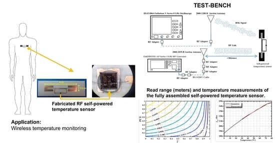
Electronics 11 01108 g030
Figure 31. Testbench used for read range and temperature characterization.
Electronics 11 01108 g031
Figure 32. Proposed self-powered sensor read range. (a) Measured read range for 65.62 mW irradiated power. (b) Extrapolated read range for 1 W irradiated power.
Electronics 11 01108 g032
Figure 33. Measured lateral sidebands by applying different temperatures in the proposed sensor. (a) Lateral sidebands generated at 35.75 °C. (b) Lateral sidebands generated at 62.5 °C. (c) Lateral sidebands generated at 72 °C.
Electronics 11 01108 g033
Figure 34. Temperature measurements of the fully assembled self-powered temperature sensor.
Electronics 11 01108 g034
Figure 35. Distribution of the power consumption of each of the subcircuits that compose the proposed sensor prototype.
Electronics 11 01108 g035
Table 1. Elements and transistor sizes of the current source core.
ElementValueElementValueElementValue
m p 1 (23.005 µm/1.8 µm) × 6 m 4 (1.8 µm/1.255 µm) m 10 11 (3.665 µm/18 µm) × 5
m p 2 (23.005 µm/1.8 µm) × 8 m 5 (1.8 µm/8.52 µm) m 12 (24.18 µm/14 µm) × 14
m p 3 (1.8 µm /0.9 µm) × 4 m 6 (5.4 µm/1.98 µm) × 14 m 13 (2.75 µm/14 µm) × 14
m 1 (13.835 µm/1.8 µm) × 4 m 7 (5.4 µm/1.885 µm) m n 1 (8.895 µm/1.8 µm) × 8
m 2 (13.835 µm/1.8 µm) × 12 m 8 (46.16 µm/0.9 µm) × 40 m n 2 (23.14 µm/1.8 µm) × 14
m 3 (1.8 µm/15.395 µm) m 9 (5.4 µm/1.9 µm) C A 1.27 pF
C B 0.5 pF
Table 2. Elements and transistor sizes of the current reference.
ElementValueElementValueElementValue
m p 1 (23.005 µm/1.8 µm) × 6 m n 1 (8.895 µm/1.8 µm) × 8 m 15 (13.835 µm/1.8 µm) × 4
m p 2 (23.005 µm/1.8 µm) × 8 m 14 (13.835 µm/1.8 µm)
Table 3. Elements and transistor sizes of the voltage reference.
ElementValueElementValueElementValue
m p 1 (23.005 µm/1.8 µm) × 6 m n 1 (8.895 µm/1.8 µm) × 8 m 16 18 (2.18 µm/9 µm) × 4
m p 2 (23.005 µm/1.8 µm) × 8 m 1 (13.835 µm/1.8 µm) × 4 m 19 (3.4 µm/18 µm)
C E 1.6 pF
Table 4. Elements and transistor sizes of the temperature sensor.
ElementValueElementValueElementValue
m p 1 (6.24 µm/1.8 µm) × 8 m 1 , m 4 (3.265 µm/3.6 µm) × 4 m 3 (7.19 µm/3.6 µm) × 4
m n 1 (16 µm/1.8 µm) × 8 m 2 (3.265 µm/3.6 µm) × 6 m 5 , m 6 (0.9 µm/0.36 µm)
Table 5. Elements and transistor sizes of the LDO voltage regulator.
ElementValueElementValueElementValue
m 1 (4.12 µm/1.8 µm) × 1 m n 1 (13.835 µm/1.8 µm) × 8 m 4 (5.355 µm/18 µm) × 4
m 2 (4.12 µm/1.8 µm) × 3 m p a s s (12.815 µm/4.5 µm) × 4 C M 2.5 pF
m e a (3.085 µm /1.8 µm) × 4 m 3 (32.99 µm/1.5 µm) × 40 C L 10 pF
Table 6. Elements and transistor sizes of the shunt regulator.
ElementValueElementValueElementValue
m 1 (11.2 µm/1.8 µm) × 25 m 4 (7.82 µm/45 µm) × 4 m 7 (7.59 µm/1.8 µm) × 10
m 2 (3.62 µm/4.5 µm) × 4 m 5 (1.375 µm/18 µm) × 2 R 1 25 K Ω
m 3 (0.9 µm/45 µm) m 6 (12.315 µm/4.5 µm) × 4
Table 7. Elements and transistor sizes of the power harvester circuit.
ElementValueElementValueElementValueElementValue
m 1 (1.5 µm/0.18 µm) × 8 L b o n d 1.5 nH @ 1 Ω L4.18 nH C L 150 pF
m 2 (1.5 µm/0.18 µm) × 4 C p a d 0.5 pF C C 2.1 pF
Table 8. Parameters of the dipole antenna.
ElementValueElementValueElementValueElementValueElementValue
A d 79.4 mm A i 30 mm L d 1 4 mm L i 11 mm S Y r b l 0.4 mm
A d 1 7.7 mm A i 1 3 mm L d 2 5 mm L i 1 1 mm
A d 2 21.7 mm L d 14 mm L d 3 1 mm S X r b l 3 mm
Table 9. Comparison with previous works.
[43][44][49][41][50][47][48][42][51][52]This Work
Technology0.35 µm0.35 µm0.25 µm0.18 µm0.18 µm0.18 µm0.18 µm0.13 µm0.13µm65 nm0.18 µm
CMOSCMOSCMOSCMOSCMOSCMOSCMOSCMOSCMOSCMOSCMOS
Chip area2.2 × 1.8 mm 2 1 × 4 mm 2 1.2 mm 2 1.2 × 2.2 mm 2 1.2 × 1.2 mm 2 0.9 × 1.1 mm 2 0.23 mm 2 0.34 mm 2 1.16 × 0.94 mm 2 1.06 × 0.56 mm 2
Full sensor1 × 4 mm 2 13 × 12 cm 2 5.6 × 5.0 cm 2 2.5 × 0.9 cm 2 1910 × 940 µm 2 8 × 2.5 cm 2
area **
Wirelessly poweredYESNOYESYESYESYESYESYESYESYESYES
Incident signal860 MHz2.5 GHz450 MHz915 MHz13.56 MHz920 MHz902–928 MHz915 MHz900 MHz79 GHz910 MHz
frequency
Wireless sensitivity−12.3 dBm−18.2 dBm−12.3 dBm−11 dBm−16 dBm−10 dBm5 dBm−8.99 dBm
Circuitry power16.85 µW ***2.75 mW1.5 µW2 µW1.05 µW8.5 µW700 µW13.75 µW
consumption
Temperature35 ∼ 4520 ∼ 90−40 ∼ 40−30 ∼ 700 ∼ 100−25 ∼ 1200 ∼ 10010 ∼ 10035 ∼ 4232 ∼ 800 ∼ 60
range ( C)
Temperature19.1 mV/ C−300 kHz/°C0.15 C/LSB−666 kHz/ C0.17 °C/LSB26 kHz/ C*−22 MHz/ C823.29 Hz/ C
sensitivity
Reader radiated2 W7 W1 W4 W4 W1 W
power (EIRP)
Read range (m)218.30.53.410.49.5
Tag-to-readerBackscatter2.5 GHz OOK2.3 GHz402 MHz OOKBackscatterBackscatterASKOOK79.1 GHz burstASK
transmission transmittertransmitter backscatter backscatterbackscattertransmitterbackscatter
CommunicationEPCOwnNotEPCNotEPCEPCNotNotNotNot
protocolGen 2protocolimplementedGen 2implementedGen 2Gen 2implementedimplementedImplementedimplemented
Not specified. * Sensitivity presents a large variation in different temperature ranges. ** Overall dimensions of the sensor includes the CMOS chip and the antenna. *** Estimated by adding the power consumption of each reported blocks (if available).
Publisher’s Note: MDPI stays neutral with regard to jurisdictional claims in published maps and institutional affiliations.

