
Bit Error Performance of APD and SPAD Receivers in Optical Wireless Communication


1
ams OSRAM, 8141 Premstätten, Austria
2
Institute of Electrodynamics, Microwave and Circuit Engineering, TU Wien, 1040 Vienna, Austria
*
Author to whom correspondence should be addressed.
Electronics 2021, 10(22), 2731; https://doi.org/10.3390/electronics10222731
Submission received: 16 September 2021
/
Revised: 4 November 2021
/
Accepted: 5 November 2021
/
Published: 9 November 2021
(This article belongs to the Special Issue Optical Wireless Communications and Networking: A Pathway towards 6G)
Abstract
:This review concentrates on the state-of-the-art hardware-oriented receiver aspects for optical wireless communication (OWC), and points to the importance of BER performance analysis and modeling in presence of non-perpendicular light incidence. Receivers in OWC networks for 6G applications have to work for strongly different light incidence angles, to allow the formation of connections to locally separated transceivers without the need for rotation units and accurate adjustment. In turn, and in combination with fully integrated optical receivers, reduction of cost and increased comfort can be achieved. Fully integrated [bipolar] complementary metal-oxide-semiconductor ([Bi]CMOS) receivers with on-chip avalanche photodiodes (APDs) and single-photon avalanche diodes (SPADs) are presented and their performance in optical wireless communication is summarized. Impressive data rates up to 2 Gbit/s and free-space transmission distances up to 27 m at bit error ratios (BER) below 10−9 are reached with linear-mode APD receivers. The importance of optical interference in the isolation and passivation stack on top of the integrated photodiodes is illuminated. To be able to predict the dependence of the BER of single-photon avalanche diode (SPAD) receivers on the light incidence angle, a model, which includes a model for the photon detection probability and a standing-wave model for the isolation and passivation stack, is extended. The dependence of the BER on the light incidence angle onto the photodiodes is investigated by electromagnetic simulation for optical transmission of the layers on top of the photodiode, device simulation for the avalanche triggering probability and BER modeling with MATLAB. It is found that incidence angles up to 30° have moderate influence on the BER and that the BER degrades significantly for incidence angles larger than 50°.
1. Introduction
Data traffic steadily increases and there is also a large growth in radio wireless communication. Optical wireless communication (OWC) [1,2,3,4], visible light communication (VLC) [5,6,7] and light fidelity (LiFi) [8,9] can take over part of the data traffic, especially indoor within rooms and offices. An advantage is a gain in comfort, when devices do not have to be connected by wires or cables. To achieve true comfort, accurate adjustment and alignment of transmitters and receivers has to be avoided and, therefore, the optical incidence angle on the receivers comes into the play. Considering the postulated need of beam steering to obtain compact and cheap devices for wireless networks [10], a wide receiver acceptance angle is also required. Receiver field-of-views between 10° and 25° are mentioned in [11]. A receiver field-of-view (FoV) of 90° was reported to be best for positioning [12]. Indeed, for practical applications of OWC and VLC, the incidence angle has large effects on the data transmission [13,14]. The importance of wide-FoV receivers for the deployment of OWC was also mentioned in [15]. However, OWC, VLC and LiFi can replace radio wireless communication in addition to homes and offices in electromagnetic interference (EMI)-sensitive environments like airplanes, hospitals, and industrial production halls [16]. Due to eye-safety reasons, the emitted optical power is quite limited and highly sensitive optical receivers with a large light-sensitive area are required for optical free-space communication.
Pulse amplitude modulation (PAM) and other efficient modulation methods for data rate enhancement were suggested [17,18,19,20]. However, according to [21], if positioning is implemented, orthogonal-frequency-division-multiplexing (OFDM) and optical code-division-multiplexing-access (OCDMA) with optical orthogonal codes [22] reduce the data rate, and the bandwidth of the photodiode limited the data rate to 2.5 Gb/s at a transmission distance of 2 m [22].
Astonishing results with respect to transmission distance were already achieved with binary pin-photodiode receivers (19 m at 3 Gb/s) exploiting a lens at the receiver [23]. The receiver lens, however, limited the total receiving angle to 9°. To compensate for the optical gain of a receiver lens, the pin-photodiode can be replaced by an avalanche photodiode (APD). Discrete APDs are optimized with respect to low excess noise. However, due to this noise reduction, they need very high reverse bias voltages (e.g., 230 V) [24]. Therefore, we investigated the possibilities of integrated APDs with thick absorption zone, so-called reach-through APDs, with respect to breakdown voltage, excess noise, and receiving angle. The results obtained with such integrated linear-mode APD receivers will be summarized below.
Since APDs were exploited excessively also as single-photon avalanche diodes in the Geiger mode for many applications including optical receivers [25,26,27] and optical free-space communication [28,29], because of their very high gain, we will also summarize the properties and results of SPAD receivers in OWC. Especially, since SPAD receivers suffer from a much larger bit-error ratio, as APD receivers, and since the bit error ratio (BER) increases with the incidence angle, the dependence of BER on the light incidence angle will be investigated.
2. Integrated APD Receivers
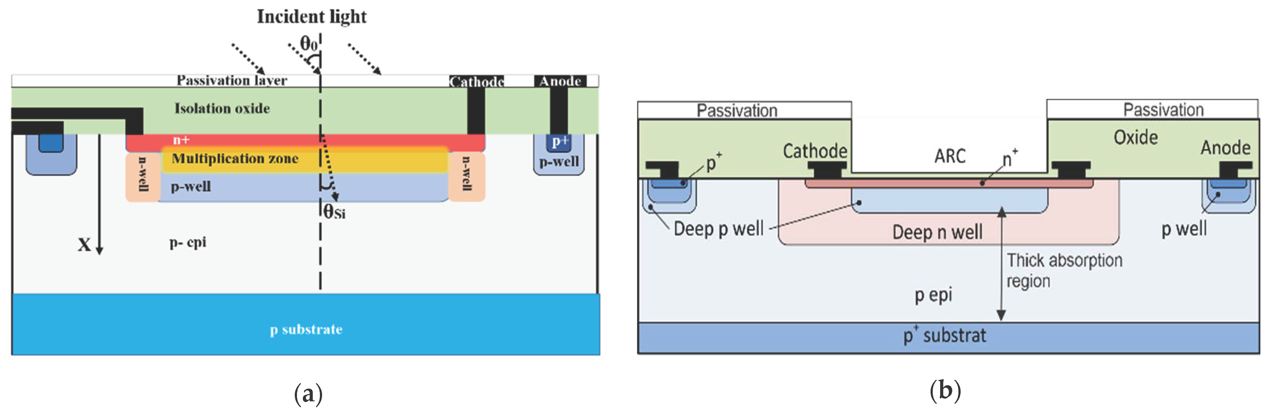
The thick absorption zone of the integrated pin photodiode in 0.35 µm (Bi)CMOS [23] was exploited for an integrated reach-through APD [30], by adding the p-well as a multiplication zone (see Figure 1a). Fortunately, the p-well of the process can be already completely depleted below the breakdown voltage, so that the thick absorption zone (p- epitaxial layer) is also fully depleted in the linear APD mode. The thickness of this intrinsic absorption zone was about 10 µm. The breakdown voltage of this pin-photodiode-(Bi)CMOS APD was about 35 V. Another possibility to obtain a thick absorption zone in a high-voltage (HV) CMOS technology was the partial compensation of the doping concentration of a deep p-well and of the p epitaxial layer, by implementation of an additional deep n-well [31] (see Figure 1b). The breakdown voltage of this HV-CMOS APD was about 68 V, which is, however, well within the isolation capability of the transistors of 100 V in this process. In contrast to the APD in pin-photodiode CMOS, the APD in HV CMOS can be equipped with an anti-reflection coating (ARC).
Via pin-photodiode APDs, with diameters of 200, 400 and 600 µm, we ended up with an 800 µm-diameter APD integrated in a 0.35 µm BiCMOS receiver [30]. A segmentation of the large-area APDs for high data rates as it was used in [32] was not necessary.
The capacitance of the 800 µm-diameter APD was 7 pF. Modulation doping of the p-well was applied in [30] to extend the bandwidth of the APD at the expense of a higher breakdown voltage. The excess noise of the HV-CMOS APD was the smallest and modulation doping increased the excess noise of the pin-photodiode APD [30]. The 200 µm-pin-APD BiCMOS optoelectronic integrated circuit (OEIC) reached a sensitivity of −32.2 dBm at a BER of 10−9 for a data rate of 2 Gbit/s (λ = 675 nm, PRBS31) [30]. The 400 µm pin-APD, accomplished −30.6 dBm [30] and the 600-µm-pin-APD BiCMOS OEIC showed a sensitivity of −29.7 dBm at 2 Gb/s (BER = 10−9).
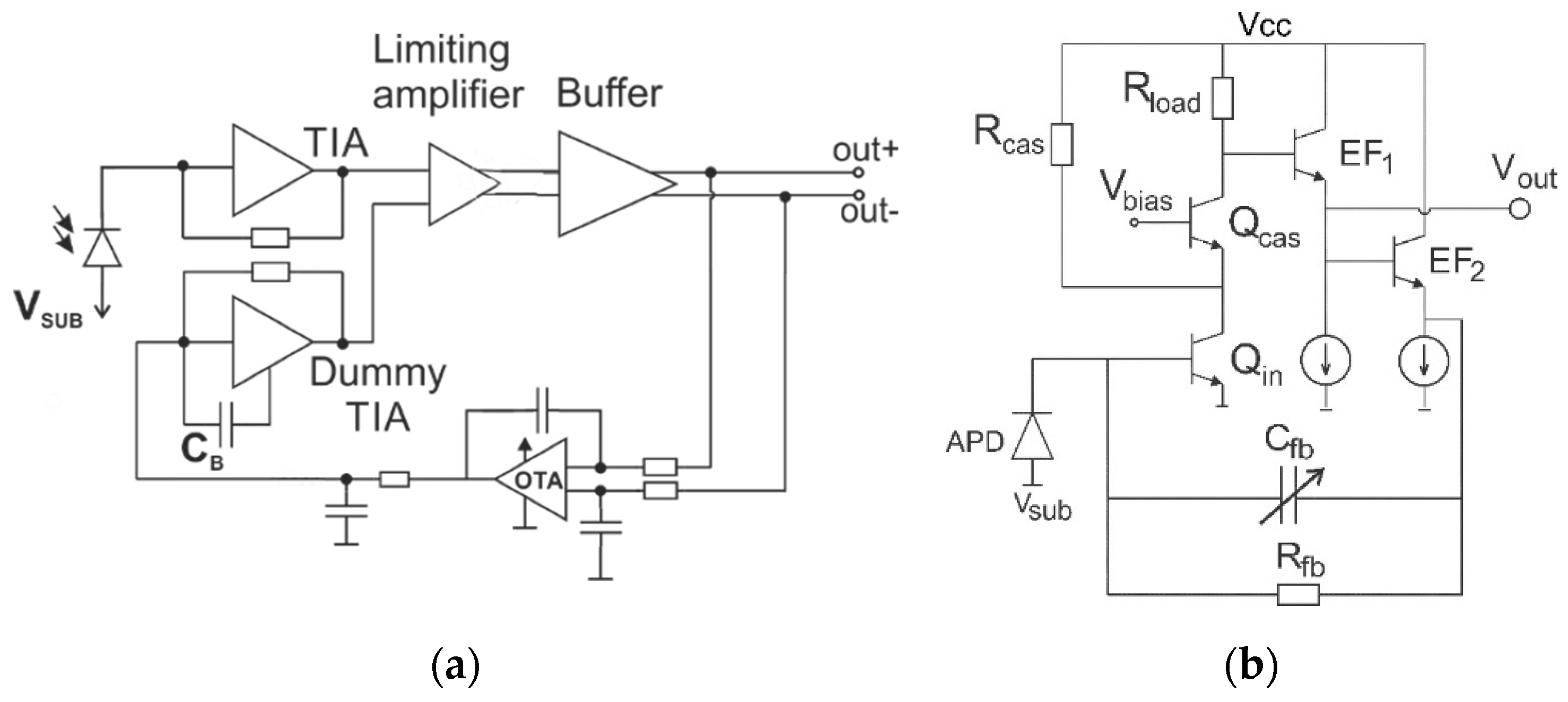
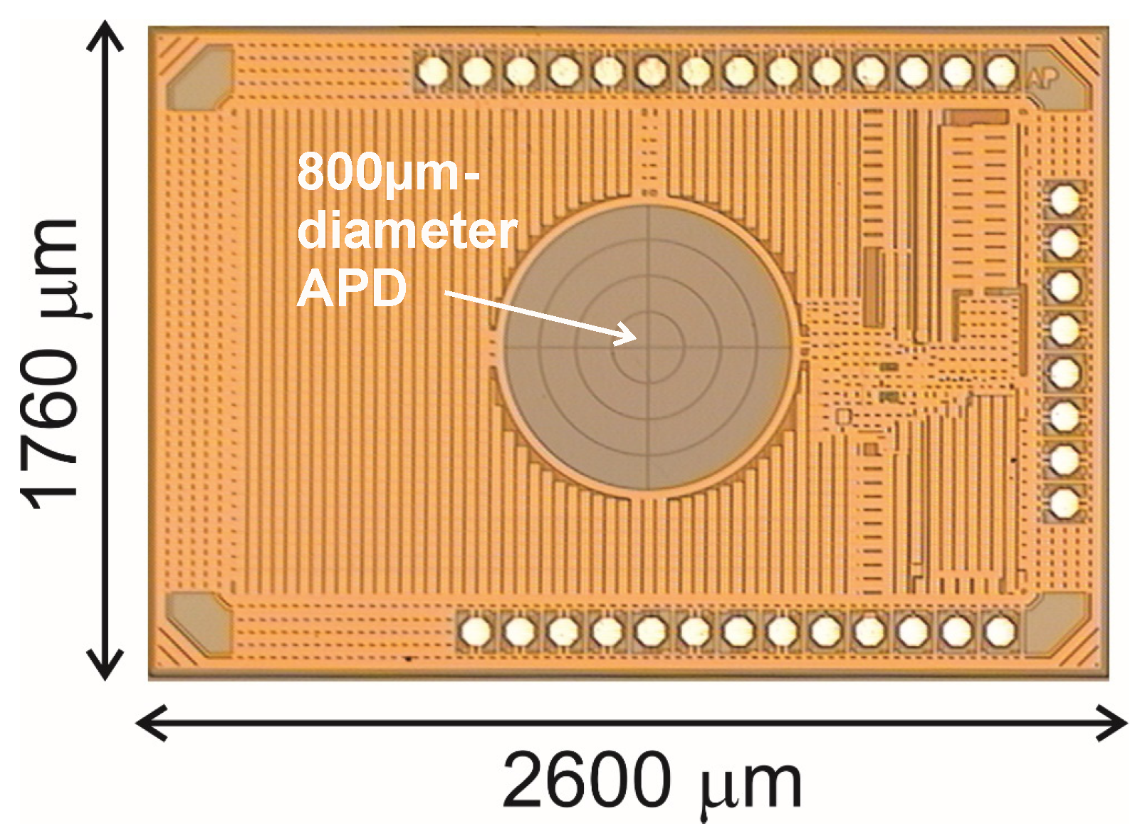
The block-diagram of the 800 µm-APD receiver is shown in Figure 2a. The dummy transimpedance amplifier (TIA) adjusts the reference voltage for the differential limiting amplifier and, together with the operational transconductance amplifier (OTA) in proportional integral (PI)-controller configuration, elimination of offset voltages and of photocurrent from background light is achieved. Noise of the dummy TIA is reduced by CB, which limits its bandwidth (for details refer to [30]). The TIA uses a cascode transistor Qcas to reduce the Miller effect, not to increase the input node capacitance further (see Figure 2b). The resistor Rcas increased the current in the input transistor Qin and thereby its transconductance for reduced input noise current. This technique allowed to keep the voltage drop across Rload low. The 3 dB bandwidth and the amount of the peaking was made tunable with the switchable capacitance Cfb (0.35 fF, 70 fF and 105 fF). A fabricated 800 µm-APD receiver chip is shown in Figure 3. The sensitivities of this 800 µm-pin-APD BiCMOS OEIC for BER = 10−9 were −33 dBm at 1 Gb/s and −29.3 dBm at 2 Gb/s [30]. It should be mentioned that, with error correction (BER = 2 × 10⁻³), the sensitivity improves by about 6 dB to −35.3 dBm at 2 Gb/s and by 5.5 dB to −38.5 dBm at 1 Gb/s [30].
Receivers with the HV-APD were realized with APD diameters of 200 and 400 µm and showed for 675 nm, 1 Gb/s, BER = 10−9, and PRBS31 sensitivities of −35.5 and −34.7 dBm [31], respectively.
3. OWC with APD Receivers
The OWC experiments were performed with a 680 nm vertical cavity surface emitting laser (VCSEL) driven with a MAX3740A chip at an optical power of 0.85 mW, and a cheap lens (MPG-95 from Roithner) for collimation of the transmitted beam to a divergence of 0.057° (full width at half maximum, FWHM) [30]. The measured transmission distances for the realized integrated APD receivers are listed in Table 1. No receiver lens was used. No 600 and 800 µm-diameter APD receivers in HV CMOS were investigated, but thanks to the anti-reflection coating (ARC), the HV CMOS APD receivers with APD diameters of 200 and 400 µm reached somewhat larger transmission distances than the pin-photodiode APD BiCMOS receivers at 1 Gb/s. The bandwidth of the HV CMOS receivers was not sufficient for 2 Gb/s. Compared to MOSFETs, bipolar transistors possess a larger transconductance at the same operating current and, therefore, the BiCMOS receivers achieved twice the data rate. With increased APD diameter, the transmission distance rose to 27 m at 1 Gb/s and to 16.5 m at 2 Gb/s.
Transmission distances up to 1.5 m and data rates reaching 3 Gb/s were published [33]. With a combination of a wire-bonded, segmented APD with an area of 10,000 µm2 in 0.35 µm technology, an ac-coupled amplifier, a transmitter lens and a receiver lens with diameters of 5–7 cm, a transmission distance of 72 m was reported for 1–2 Gb/s [34]. The sensitivity for BER = 3.8 × 10⁻³ at 680 nm was given with −30 dBm. In [35], the transmission distance was 2 m with a VCSEL as transmitter, a photodiode being 65 µm in square and a data rate of 50 Mb/s. With visible and infrared LED for down- and up-link, respectively, 400 Mb/s was transmitted via 2 m at a BER of 10−8 using discrete multi-tone (DMT) [36]. A data rate of 11.1 Gb/s was transmitted over 1.2 m free-space distance with a 682 nm, 1 GHz VCSEL, a 2 GHz APD using OFDM and a parallel beam [37].
The bit error ratio (BER) was also investigated in dependence on the light incidence angle. Compared to the pin-photodiode receiver with receiver lens, the receiving angle for a BER < 10−9 was doubled to 18° for the pin-photodiode 400 µm-APD receiver without receiver lens at a data rate of 2 Gb/s and a distance of 11 m [38]. The “oscillations” of the BER, in dependence on the light incidence angle, and the increase of the BER, with the incidence angle for the APD receiver without ARC [38], actually were the motivation to investigate the BER of SPAD receivers in dependence on the light incidence angle. The maximum light receiving angle was 76° (±38°, 200 µm-APD at 11 m distance) and 74° (±37°, 400 µm-APD at 20 m distance), both at 1 Gb/s, thanks to the ARC being disposable in the 0.35 µm HV CMOS process [31]. If error correction is used, the BER can raise up to 2 × 10⁻³ [39,40] and the total receiving angles are larger than 124° and 144° for the HV-CMOS APD receiver and the pin-photodiode CMOS APD receiver [30], respectively.
4. SPAD Receivers
The first SPAD receiver was introduced in 2013 [25]. This receiver contained 1024 thin p+/n-well SPADs and its sensitivity for 100 Mb/s and 450 nm was −31.7 dBm. The next one implemented 100 SPADs and achieved 20 Mb/s at a wavelength of 860 nm without reporting a sensitivity [41]. For 100 kb/s, the reported sensitivity was −64 dBm [17]. In [18] the data rate was raised to 200 kb/s and at 1 kb/s the sensitivity was −107 dBm.
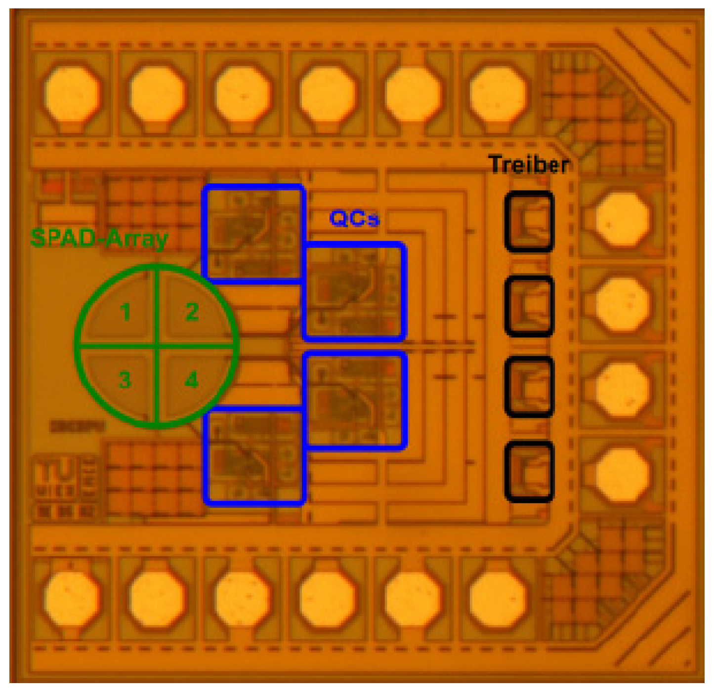
The APD in pin-photodiode CMOS (see Figure 1a) can also be operated in the Geiger mode, and four SPADs of this type were implemented together with active quenching circuits in 0.35 µm CMOS for an excess bias of 6.6 V [42]. A low avalanche detection threshold and a fast quenching reaction time were achieved by a sensitive comparator and pre-biasing, respectively, in order to keep afterpulses low. There are also dark counts in SPADs. Both, afterpulses and dark counts lead to a high BER, if only one SPAD is used in an optical receiver. In order to reduce the probability of bit errors, a coincidence principle can be used, however, at the expense of detection of a photon each in a few SPADs. But within arrays of SPADs, there is another parasitic effect, namely optical crosstalk, which is also relevant for the BER. The first guess for our SPAD’s dark count rate (DCR) and afterpulsing probability (APP) behavior was that four SPADs should be sufficient to push the BER below the forward error correction (FEC) limit of 2 × 10⁻³. The measured sensitivity of this 4-SPAD receiver for this BER was −54 dBm in NRZ and −55.7 dBm in RZ, both for 50 Mb/s, using analog postprocessing in MATLAB [42]. The data rate of the 4-SPAD receivers is mainly limited by the dead time, which is necessary to keep BER caused by afterpulses low enough for error correction.
Since experiments on the few-photon level are very complex and time consuming, we developed a BER model for SPAD receivers [43], considering the measured parasitic SPAD noise [44]. The BER model can help us to better understand the contribution of different SPAD intrinsic parasitics to the receiver performance and identify the bottleneck to enable further circuit and device structure optimizations. In fact, even by complex and time consuming experimental investigation it is hard to distinguish between the bit errors caused by dark count, afterpulsing and crosstalk noise mechanisms. A very important result of a sensitivity analysis using the BER model was that the optical crosstalk influences the BER more severely, as compared to the afterpulsing and dark count mechanisms [43]. Therefore, BER models that describe single-SPAD receivers [45] or neglect the crosstalk effect in SPAD arrays [25,46] are not applicable here.
The BER model presented in [43] is based on the calculation of error probabilities assuming equally likely bits “0” and “1,” where the receiver decides for a logical bit “0” or “1” by comparing the number of triggered SPADs to a decision threshold during each bit time. Our experimental investigation on the 4-SPAD receiver (Figure 4) showed that a decision threshold of four (triggered) SPADs can overcome the parasitic effects to provide an acceptable BER (<2 × 10⁻³) [43].
A wrong decision with regard to a logical “1” bit happens when less than four SPADs fire during the bit time. At a given optical power, the error probability can be decreased by increasing the excess bias voltage on the SPADs to increase the photon detection probability (PDP). However, this will also increase the noise (i.e., the avalanche probabilities associated with the background light, dark count, afterpulsing, and crosstalk), which increases the possibility for incorrect decisions with respect to logical “0” bits. Therefore, there is an optimum excess bias voltage level corresponding to a minimum total error probability (for both of logical “0” and “1” bits) at a specific optical power level.
The BER model can capture the contribution of photon absorption, dark-count, afterpulsing, and crosstalk avalanche triggering mechanisms to the total detection and error probabilities in all SPADs as explained in detail in [43]. The model assumes that the SPAD intrinsic noise is independent of the optical signal (i.e., receiving a logical “0” or “1”), as the noise avalanche triggering probability in a ready-to-fire SPAD during a given bit time does not depend on the current incident optical power. Therefore, in order to extend this model to incorporate the effect of a deviation in the light incidence angle from the surface normal on the BER performance, we only need to modify the photo-count statistics. In order to apply this modification, we need to characterize the dependency of the photon detection probability (PDP) on the light incidence angle at any specific wavelength, and this requires a PDP model that carefully characterizes the dependency of the PDP on different optical and electrical parameters. We presented a comprehensive PDP model in [47] that can capture the dependency of the PDP on the angular deviation of the incident light, and in Section 6 we explain how these models can be used to predict the BER performance of SPAD receivers.
5. OWC with SPAD Receivers
We should also be aware that background light acts like dark counts in SPAD receivers during OWC (i.e., it increases the BER). Therefore, it is indispensable to use an optical interference filter for OWC with SPAD receivers. What is more, SPAD receivers are characterized by much higher BERs than APD receivers. APD receivers can be used in error-free operation (BER < 10−9). SPAD receivers; however, have BERs being orders of magnitude larger, although a coincidence principle is used. Nevertheless, the SPAD receiver presented in Figure 4 was tested in OWC. A 650 nm 1.1 mW resonant cavity (RC) light emitting diode (LED) from Firecomms and a collimating lens were used [48]. In non-return to zero (NRZ) with the 4-SPAD receiver, the maximum distance at 50 Mb/s for a BER below the forward error correction (FEC) limit was 5 m. The influence of the return-to-zero (RZ) duty cycle on the BER was investigated in [48]. It was possible to increase the data rate to 75 Mb/s at a distance of 3 m. Lowest BERs were obtained at duty ratios of about 50%. When we compare SPAD receivers with APD receivers with respect to transmission distance, SPAD receivers are inferior, although they possess a better sensitivity.
To come back to the high BER of SPAD receivers: When we envision the dependence of the BER of linear-mode APD receivers on the light incidence angle (i.e., the increase of the BER with the incidence angle), such a behavior can become a severe problem for SPAD receivers. Since the BER of the SPAD receivers is not far away from the FEC limit, the receiving angle of SPAD receivers may be severely limited. To investigate this issue, we developed a BER model also in dependence on the light incidence angle for SPAD receivers. Since DCR, APP and optical crosstalk of SPADs are independent of the light incidence angle, only the dependence of the PDP on the incidence angle is needed for the usage of the BER model reported in [43].
6. PDP and BER of SPAD Receivers in Dependence on Light Incidence Angle
As it was mentioned before, in order to consider the effect of the deviations in the light incidence angle from the surface normal on the BER performance, we need to modify the photo-count statistics by characterizing the angular dependency of the PDP. The BER model presented in [43] assumes that, similar to the SPAD noise detection probability, the photon detection probability is only a function of the SPAD biasing condition. This is a reasonable assumption if the modeling is used to characterize the BER at perpendicular light incidence condition. However, the effect of the deviations in the light incidence angle cannot be captured unless the BER modeling approach is extended to take this effect into account.
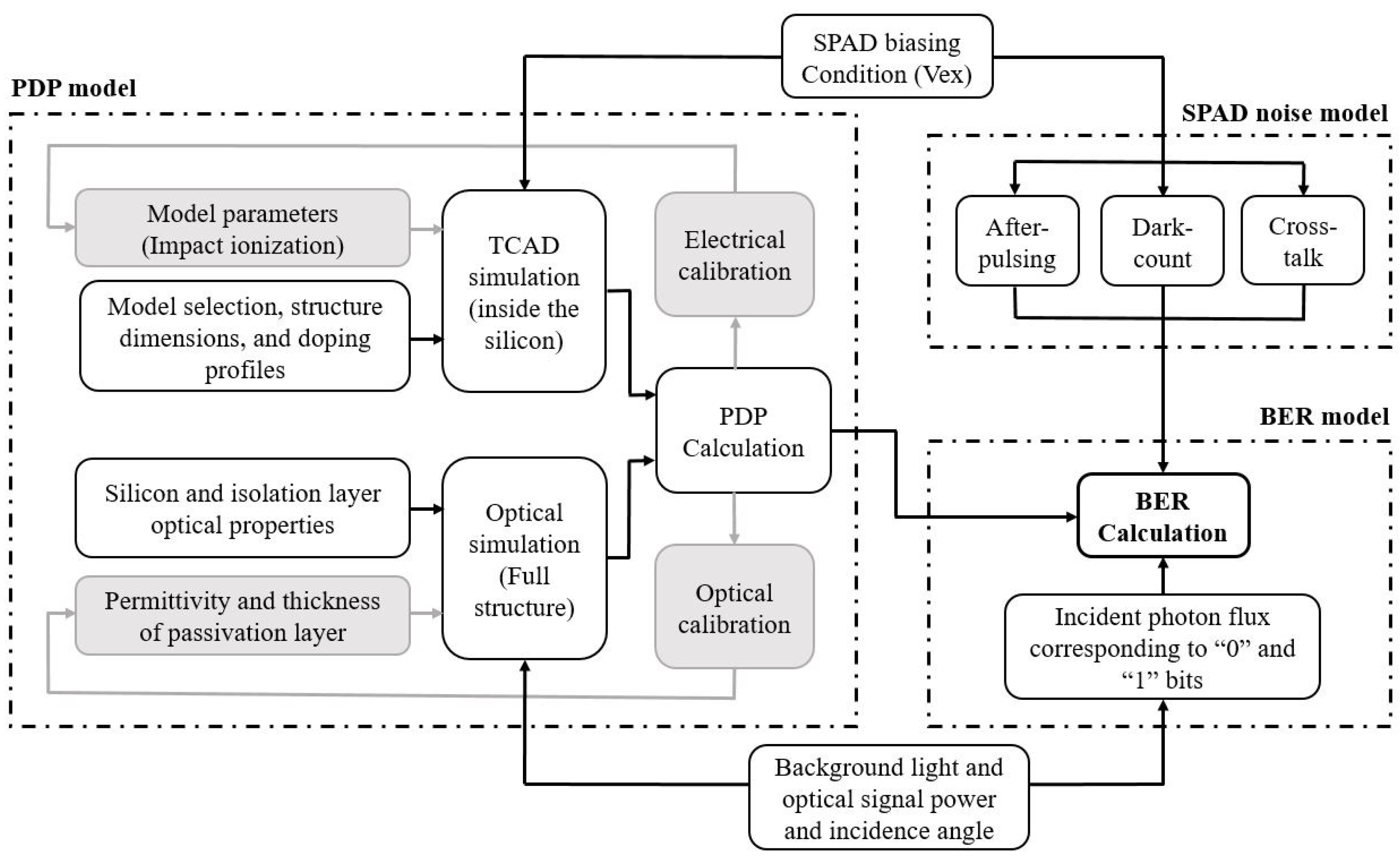
In order to characterize the PDP performance of SPAD devices, a physics-motivated approach can be used based on the characterization of the avalanche triggering probability inside the silicon [49,50,51,52]. However, here we need a comprehensive PDP modeling approach that accurately considers the photon absorption profile inside the silicon region in presence of angular deviation as is presented in [47]. Therefore, we employ this PDP model and extend the BER model according to Figure 5, where a flow chart of the proposed methodology for accurate modeling of the BER performance of a SPAD array receiver is presented. In this extended mode, different electrical and optical effects including the angular deviation of the incident light from the surface normal are taken into account.
Here, the SPAD biasing condition and the photon incidence angle are provided to the PDP model to obtain avalanche triggering probability and photon absorption probability profile inside the silicon, using TCAD (ATLAS from Silvaco [53]) and electromagnetic simulation (optical simulation) with CST [54], respectively. Accordingly, the photon detection probability of the SPAD is obtained and, therefore, the photon-count statistics in presence of the light incidence angle can be determined to allow the BER model to take this effect into account. In fact, an angular deviation of the light incidence (θ) from the surface normal affects the photon absorption probability profile, as it changes the photon transmission into the silicon as well as the absorption depth of the transmitted photons inside the silicon. However, the TCAD simulation results to obtain the avalanche triggering probability are independent of θ, as θ only affects the photon transmission into the silicon, but not the electric field profile inside the silicon. In order to obtain the photon transmission as a function of θ using electromagnetic simulations, we need to know the optical properties of the silicon and of the layers above as they have a significant influence on the photon transmission. In this SPAD technology, the silicon is covered with isolation and passivation stacks and it is important to note that the PDP model requires electrical and optical calibration, where unknown parameters are extracted by fitting to measurement data. For example, in [47] it is explained how the exact values of the thickness and the refractive index of these layers are extracted using a calibration of optical properties of the structure to conduct accurate optical simulations. Furthermore, an accurate BER model requires careful SPAD noise characterization and modeling, where the probability of noise detection due to each noise mechanism is modeled as a function of the SPAD excess bias voltage. In [44], an extensive empirical study is presented to model dark-count, afterpulsing, and crosstalk for SPAD arrays based on experimental data acquired in dark condition. We employ this approach to accurately introduce the noise contribution into the BER performance. This allows to distinguish the individual contribution of different noise mechanisms at different receiver operation conditions.
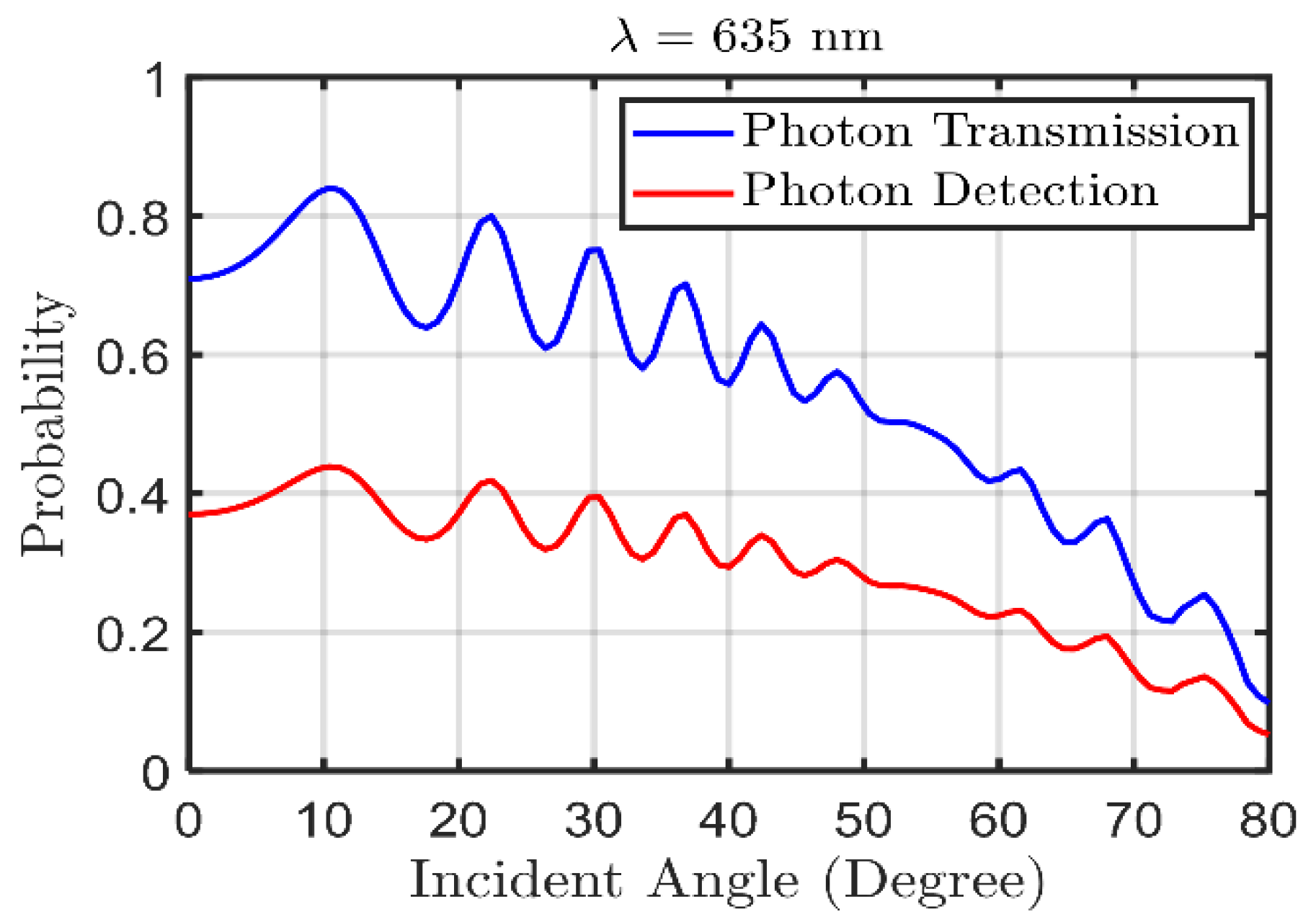
In general, we expect that the PDP deceases with increasing θ as the reflection increases and less photons are transmitted into the silicon. Figure 6 shows the dependency of the photon transmission and photon detection probabilities on the light incidence angle. Here, we see that the transmission spectrum shows a decrease with θ but also some fluctuations with θ. The fluctuations are due to the formation of standing waves in the isolation and passivation stack caused by destructive and constructive interference of multiple reflections of light at the interfaces. Therefore, at smaller θ (<10° as shown for λ = 635 nm in Figure 6), the PDP is increasing with θ as it corresponds to a small increase of the length of the light trajectory inside the isolation layer, reaching a local maximum of the transmission into silicon at about 10°.
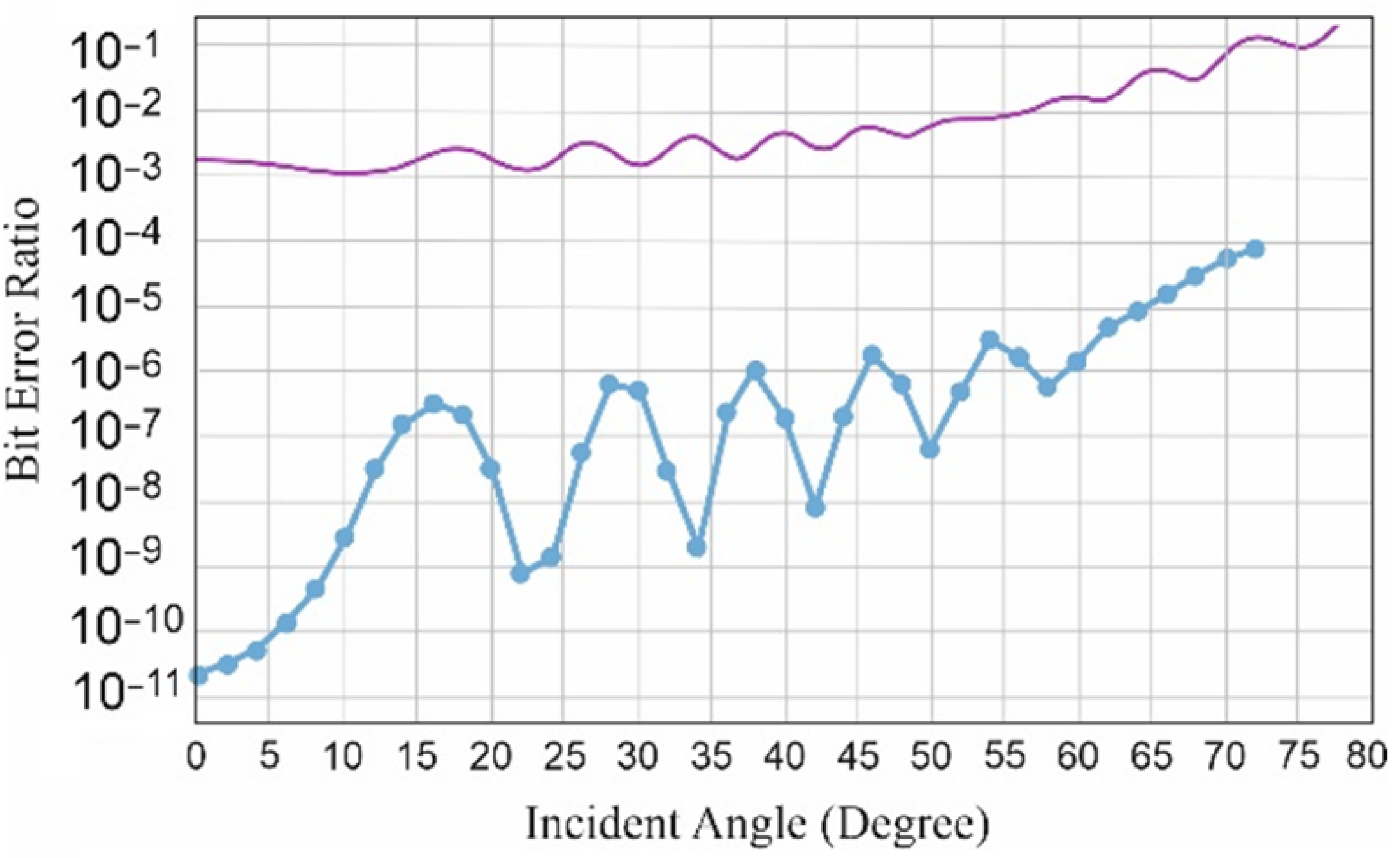
The results of the angular-dependent BER modeling for the SPAD receiver are shown in Figure 7 as the upper curve assuming a non-return to zero (50% duty cycle) optical signal of an average power equal to 5 nW (i.e., ~320 photons per bit at 50 Mbit/s) on the 4-SPAD receiver with a decision threshold of four-out-of-four for logical “1”. To provide a vivid comparison of the BER of SPAD receivers to that of APD receivers, the BER profile of the APD from [38] is plotted into Figure 7 as the lower curve. This comparison indicates that the BER of the SPAD receiver is several orders of magnitude larger than the BER of the APD receiver, with the same isolation and passivation stack in the pin-photodiode CMOS technology.
According to the simulation results shown in Figure 6, both transmission and PDP are decreased by around 50% when the angular deviation is increased to θ = 60°, and this corresponds to a degradation of around one order of magnitude in the BER performance as is shown in Figure 7 (upper curve). That means, in order to have a maximum detection angle of θ = 60°, one needs to keep the BER smaller than 2 × 10⁻⁴ at θ = 0° to provide a BER of 2 × 10⁻³ at θ = 60°. The results shown in Figure 7 indicate that an angular deviation below θ = 30° shows a moderate effect on the BER performance of the 4-SPAD receiver, while incidence angles θ > 50° will impose significant degradations.
7. Discussion
There are APDs consisting of p+ and n-well or deep n-well [55,56] and consisting of n+ and p-well inside a deep n-well [57,58] in the literature. However, for red and near-infrared wavelengths, due to the small thickness of the wells, only a (small) part of the photogenerated carriers can be multiplied by impact ionization, and their responsivity is much lower than that of the thick pin-photodiode and high-voltage CMOS APDs introduced in Section 2. Spatially-modulated-light detectors [59,60] were applied to eliminate the effects of slow carrier diffusion. They, however, suffer also from a low responsivity of the photodetector in 0.18 and 0.13 µm CMOS, respectively.
There are receivers with integrated photodiodes for operation in the Gb/s-regime in advanced CMOS [61,62,63,64,65,66,67]. However, they achieve low sensitivities (−10.65 dBm at 0.6 Gb/s [61], −3.87 dBm at 4 Gb/s [62], −3.67 dbm at 5 Gb/s [59], −5.5 dBm at 4.25 Gb/s [63], −4.4 dBm at 4.5 Gb/s [60], −3.2 dBm at 8.5 Gb/s [64], −4 dBm at 10 Gb/s [65], −6 dBm at 10 Gb/s [66], and −2 dBm at 12.5 Gb/s [67]), because of the small responsivities of the shallow photodiodes and wells in these technologies. The sensitivities of the integrated APD receivers in 0.35 µm (Bi)CMOS are two to three orders of magnitude better due to their thick absorption zone, however, at the expense of the data rate limitation to 1 or 2 Gb/s. These APD receivers cannot reach the data rate of the pin-photodiode receiver of 3 Gb/s in the same technology node [23] because of the avalanche build-up time.
The sensitivity of a linear-mode large-area APD receiver was −38.5 dBm at 155 Mb/s [68]. A receiver with a discrete 1.95 mm-diameter APD needed an optical power of −38 dBm at 280 Mb/s [1]. It is important to mention that a 20 dB better sensitivity translates to a factor of 10 in OWC transmission distance. Compared to [1,68] with comparable sensitivities, the data rate of the integrated APD receivers in 0.35 µm technology is enhanced considerably. An imaging receiver consisting of seven InGaAs MSM (metal-semiconductor-metal) flip-chip bonded photodiodes (with a responsivity of 0.4 A/W) and an amplifier in 0.18 µm CMOS showed a sensitivity of −16.8 dBm at 5 Gb/s [69], whereby the seven photocurrents were added by current mirror circuits. With a 4 × 4 photodiode matrix (each photodiode with a diameter of 215 µm) packaged in a TO−5 can and a commercial TIA, a sensitivity of about −34 dBm at 1 Gb/s and a BER of 10−3 with a receiver field of view of 10° was reported [70].
In 0.13 µm CMOS image sensor (CIS) technology, a 64 × 64 SPAD receiver was reported [26]. The large amount of SPADs enables dead times longer than a bit duration to reduce the afterpulsing probability and in turn the bit error ratio at higher data rates. Passively quenched, thin SPADs and digital signal processing were implemented. A sensitivity of −49.9 dBm at 400 Mb/s with 450 nm light and on-off keying was reported. A 500 Mb/s data rate was achieved with 4-PAM transmission at an optical power of −46.1 dBm. This SPAD receiver realized a remaining gap to the Poisson limit (quantum limit) of 11.1 dB for 50 Mb/s and 13.4 dB for 100 Mb/s and 450 nm [27]. There were also silicon photomultiplier (SiPM) receivers published [71,72], where sensitivities of −53.4 dBm at 400 Mb/s and −49 dBm at 1 Gb/s with 405 nm light were reported. These approaches may be further developed for OWC applications.
A receiver with 60 SPADs reached 200 Mb/s over a very short distance [17]. A 2 m transmission distance at a data rate of 60 Mb/s exploiting three 128 × 32 SPAD array receivers for 20 Mb/s each was suggested [18]. Compared to these OWC experiments, the 4-SPAD receiver performs quite well in OWC with transmission distances of up to 5.3 m.
It should be mentioned that not only the oxidation and passivation stack or the ARC layer on top of the SPAD are important for the light incidence angle. To reduce photon detections from ambient light, an optical narrow band filter (interference filter) is necessary in front of the SPAD receiver. Since the transmission band of interference filters depends on the light incidence angle, an additional limitation for the incidence angle on SPAD receivers in OWC applications exists.
8. Conclusions
The linear-mode APD receivers in 0.35 µm HV CMOS and 0.35 µm BiCMOS discussed above achieve high data rates (1 and 2 Gb/s, respectively), with BER = 10−9 at distances to the quantum limit of 19.6 dB [31]. When allowing a BER of 2 × 10⁻³, their sensitivities improve by about 5 dB (the gap to the quantum limit stays the same, because the quantum limit changes also by 5 dB). In OWC, these APD receivers work over transmission distances of 12.2 and 11 m, respectively, both at 1 Gb/s, with a 200 µm diameter of the APD and BER = 10−9. The SPAD array of the 4-SPAD receiver in 0.35 µm CMOS also had a diameter of 200 µm, but the fill factor was about 50% [42]. However, this does not completely explain the maximum transmission distance of the 4-SPAD receiver of 5 m at 50 Mb/s. The dead time of about 9 ns of the SPADs in the SPAD receiver explains another part of the difference in transmission distance. The light-sensitive area of SPAD receivers cannot be increased to enable larger transmission distances with SPAD receivers, because more bit errors for the logical zero will be generated by photons from ambient light and because an interference filter in front of the receiver has already been used. A larger light-sensitive area of SPAD receivers also increases the DCR, APP and optical crosstalk, which all increase the BER. In contrast, the diameter of the APDs in linear-mode APD receivers was increased to 800 µm and indoor OWC was verified up to about 2 klx ambient light at transmission distances up to 16.5 m at 2 Gb/s and up to 27 m at 1 Gb/s without receiver lens and without optical filter at the receivers [30].
Another very large difference between APD receivers and SPAD receivers is the very large difference of the possible data rates. The data rate of the 4-SPAD receivers is mainly limited by the dead time, which is necessary to keep bit errors from afterpulses low. A way out of this limitation was presented in [26] with a 64 × 64-SPAD receiver, which allows shorter bit periods than the dead time, since enough SPADs are still available for detections at low light levels. However, the data rates published for this multi-SPAD receiver of 400 and 500 Mb/s are still two to four times lower than the data rate of 0.35 µm (Bi)CMOS APD receivers, although it was realized in 0.13 µm CMOS. The gap to the quantum limit of the multi-SPAD receiver of [26] was about 12.2 dB. These results show that there is still a long way to high-data rate SPAD receivers. The SiPM receivers of [71,72] should also be further developed and investigated in OWC applications.
After experimental determination of DCR, APP and optical crosstalk for the SPADs in the receiver array, the BER model for SPAD receivers describes the measured dependency of BER on optical input power very well. The needed PDP can be determined quite reliably by electromagnetic and TCAD simulation. Since DCR, APP and especially optical crosstalk between the SPADs depend strongly on the geometrical arrangement of the SPADs (size, pitch and gap between the SPADs), they are less accurately predictable. For DCR and APP it may be an acceptable approach to assume these effects proportional to the area of the p/n-junction of the multiplication region. However, a model for the light emission spectrum and the total number of photons being emitted during a Geiger mode event in dependence on doping and excess bias voltage to calculate the probability of the optical crosstalk is missing for an a priori modelling of the BER of SPAD receivers.
The models and simulation results are limited to room temperature characterization. Taking the temperature effect into account will need considerable extra effort and consideration (temperature dependence of PDP, DCR, APP, and crosstalk) and will affect the simulation results; however, the same simulation approach can be employed.
The PDP model for SPADs and the BER model for SPAD receivers represent further steps to the improvement of SPAD receivers. The advancement of these models by considering the light incidence angle can save much time and costs for developing SPAD receivers which are easy to arrange in practical OWC settings. The isolation and passivation stack of the pin-photodiode CMOS SPAD receiver limits the light incidence angle to about 30°. Therefore, we recommend an anti-reflection coating especially for OWC SPAD receivers to allow also for larger incidence angles.
Author Contributions
Conceptualization, H.M. and H.Z.; methodology, validation, analysis, investigation, and data curation of PDP and BER models, H.M.; writing—original draft preparation, H.M. and H.Z.; writing—review and editing, H.M. and H.Z.; project administration, H.Z.; funding acquisition, H.Z. All authors have read and agreed to the published version of the manuscript.
Funding
This research was funded partially by the Austrian Science Fund (FWF), grant numbers P 28335-N30 and P 32393-N30.
Institutional Review Board Statement
Not applicable.
Informed Consent Statement
Not applicable.
Data Availability Statement
Acknowledgments
The authors thank K. Schneider-Hornstein and S. S. Kohneh Poushi for the help with some figure preparations.
Conflicts of Interest
The authors declare no conflict of interest.
References
- O’Brien, D.; Turnbull, R.; Le Minh, H.; Faulkner, G.; Bouchet, O.; Porcon, P.; Li, J. High-speed optical wireless demonstrators: Conclusions and future directions. J. Lightw. Technol. 2012, 30, 2181–2187. [Google Scholar] [CrossRef] [Green Version]
- Haas, H.; Elmirghani, J.; White, I. Optical wireless communication. Philos. Trans. A 2020, 378, 20200051. [Google Scholar] [CrossRef] [PubMed] [Green Version]
- Jungnickel, V.; Forck, A.; Haustein, T.; Krüger, U.; Pohl, V.; von Helmolt, C. Electronic tracking for wireless infrared communications. IEEE Trans. Wireless Commun. 2003, 2, 989–999. [Google Scholar] [CrossRef]
- Hinrichs, M.; Berenguer, P.W.; Hilt, J.; Hellwig, P.; Schulz, D.; Parskevopoulos, A.; Bober, K.L.; Freund, R.; Jungnickel, V. A physical layer for low power optical wireless communications. IEEE Trans. Green Commun. Netw. 2021, 5, 4–17. [Google Scholar] [CrossRef]
- Karunatilaka, D.; Zafar, F.; Kalavally, V.; Parthiban, R. LED based indoor visible light communications: State of the art. IEEE Commun. Surv. Tutor. 2015, 17, 1649–1678. [Google Scholar] [CrossRef]
- Komine, T.; Nakagawa, M. Fundamental analysis for visible-light communication system using LED lights. IEEE Trans. Consum. Electron. 2004, 50, 100–107. [Google Scholar] [CrossRef]
- Ghassemlooy, Z.; Alves, L.N.; Zvánovec, S.; Khalighi, M.A. (Eds.) Visible Light Communications, Theory and Applications; CRC Press: Boca Raton, FL, USA, 2017. [Google Scholar]
- Borkute, A.; Padole, A. Light fidelity—The future technology in wireless communication. Int. J. Sci. Eng. Res. 2013, 4, 153–161. [Google Scholar]
- Kouhini, S.M.; Kottke, C.; Ma, Z.; Freund, R.; Jungnickel, V.; Müller, M.; Behnke, D.; Vazquez, M.M.; Linnartz, J.-P.M.G. LiFi positioning for industry 4.0. IEEE J. Sel. Top. Quantum Electron. 2021, 27, 7701215. [Google Scholar]
- Wolf, M.; Li, J.; Grobe, L.; O’Brien, D.; Minh, H.L.; Bouchet, O. Challenges in GBPS wireless optical transmission. Mobile Lightweight Wireless Systems, Mobilight 2010. In Lecture Notes of the Institute for Computer Sciences, Social Informatics and Telecommunications Engineering; Chatzimisio, P., Verikoukis, C., Santamaría, I., Laddomada, M., Hoffmann, O., Eds.; Springer: Berlin/Heidelberg, Germany, 2010; Volume 45, pp. 484–495. [Google Scholar]
- Zhuang, Y.; Hua, L.; Qi, L.; Yang, J.; Cao, P.; Cao, Y.; Wu, Y.; Thompson, J. and Haas, H. A survey of positioning system using visible LED lights. IEEE Commun. Surv. Tutor. 2018, 20, 1963–1988. [Google Scholar] [CrossRef] [Green Version]
- Prince, J.G.B.; Little, T.D.C. A two phase hybrid RSS/AoA algorithm for indoor device localization using visible light. In Proceedings of the IEEE Global Communications Conference (GLOBECOM), Anaheim, CA, USA, 3–7 December 2012; pp. 3347–3352. [Google Scholar]
- Woo, T.; Park, J.K.; Kim, J.T. Effects of incident angle and distance on visible light communication. Int. J. Electron. Commun. Eng. 2017, 11, 70–73. [Google Scholar]
- Ju, M.; Huang, P.; Li, Y.; Shi, H. Effect of receiver’s tilted angle on the capacity for underwater wireless optical communication. MDPI Electron. 2020, 9, 2072. [Google Scholar] [CrossRef]
- Jenila, C.; Jeyachitra, R.K. Green indoor optical wireless communication systems: Pathway towards pervasive deployment. Digit. Commun. Netw. 2021, 7, 410–444. [Google Scholar] [CrossRef]
- Paraskevopoulos, A.; Vucic, J.; Voß, S.-H.; Swoboda, R.; Langer, K.-D. Optical wireless communication systems in the Mb/s to Gb/s range, suitable for industrial applications. IEEE Trans. Mechatron. 2010, 15, 541–547. [Google Scholar] [CrossRef]
- Almer, O.; Tsonev, D.; Dutton, N.A.; Al Abbas, T.; Videv, S.; Gnecchi, S.; Henderson, R.K. A SPAD-based visible light communications receiver employing higher order modulation. In Proceedings of the 2015 IEEE Global Communications Conference (GLOBECOM), San Diego, CA, USA, 6–10 December 2015; pp. 1–6. [Google Scholar]
- Almer, O.; Dutton, N.A.W.; Abbas, T.A.; Gnecchi, S.; Henderson, R.K. 4-PAM visible light communications with a XOR-tree digital silicon photomultiplier. IEEE Summer Top. Meet. Ser. 2015, 41–42. [Google Scholar]
- Khalighi, M.A.; Long, S.; Bourennane, S.; Ghassemlooy, Z. PAM and CAP-based transmission schemes for visible-light communications. IEEE Access J. Spec. Issue Opt. Wirel. Technol. 5G Commun. Beyond 2017, 5, 27002–27013. [Google Scholar] [CrossRef]
- Li, Y.; Safari, M.; Henderson, R.; Haas, H. Optical OFDM with single-photon avalanche diode. IEEE Photonics Technol. Lett. 2015, 27, 943–946. [Google Scholar] [CrossRef]
- Wang, K.; Song, T.; Kandeepan, S.; Li, H.; Alameh, K. Indoor optical wireless communication system with continuous and simultaneous positioning. Opt. Express 2021, 29, 4582–4595. [Google Scholar] [CrossRef] [PubMed]
- Yamaguchi, S.; Mai, V.V.; Thang, T.C.; Pham, A.T. Design and performance evaluation of VLC indoor positioning system using optical orthogonal codes. In Proceedings of the IEEE Fifth International Conference on Communications and Electronics (ICCE), Danang, Vietnam, 30 July–1 August 2014; pp. 54–59. [Google Scholar]
- Brandl, P.; Schidl, S.; Zimmermann, H. PIN-photodiode optoelectronic integrated receiver used for 3-Gb/s free-space optical communication. IEEE J. Sel. Top. Quantum Electron. 2014, 20, 6000510. [Google Scholar] [CrossRef]
- Silicon Avalanche Photodiode SAE-Series (Red-Enhanced). Available online: lasercomponents.com (accessed on 14 May 2021).
- Fisher, E.; Underwood, I.; Henderson, R. A reconfigurable single-photon-counting integrating receiver for optical communications. IEEE J. Solid-State Circuits 2013, 48, 1638–1650. [Google Scholar] [CrossRef]
- Kosman, J.; Almer, O.; Abbas, T.A.; Dutton, N.; Walker, R.; Videv, S.; Moore, K.; Haas, H.; Henderson, R. A 500Mb/s -46.1dBm CMOS SPAD receiver for laser diode visible-light communication. In Proceedings of the IEEE ISSCC, San Francisco, CA, USA, 17–21 February 2019; pp. 468–469. [Google Scholar]
- Griffith, A.D.; Herrnsdorf, J.; Almer, O.; Henderson, R.K.; Strain, M.J.; Dawson, M.D. High-sensitivity free space optical communications using low size, weight and power hardware. arXiv 2019, arXiv:1902.00495. [Google Scholar]
- Chitnis, D.; Zhang, L.; Chun, H.; Rajbhandari, S.; Faulkner, G.; O’Brien, D.; Collins, S. A 200Mb/s VLC demonstration with a SPAD based receiver. In Proceedings of the 2015 IEEE Summer Topicals Meeting Series (SUM), Nassau, Bahamas, 13–15 July 2015; pp. 226–227. [Google Scholar]
- Kosman, J.; Almer, O.; Jalajakumari, A.V.N.; Videv, S.; Haas, H.; Henderson, R.K. 60Mb/s, 2 m visible light communications in 1klx ambient using an unlensed CMOS SPAD receiver. In Proceedings of the 2016 IEEE Photonics Society Summer Topical Meeting Series (SUM), Newport Beach, CA, USA, 1–13 July 2016; pp. 171–172. [Google Scholar]
- Milovancev, D.; Jukic, T.; Vokic, N.; Brandl, P.; Steindl, B.; Zimmermann, H. VLC using 800-µm diameter APD receiver integrated in standard 0.35-µm BiCMOS technology. IEEE Photonics J. 2021, 13, 7900513. [Google Scholar] [CrossRef]
- Milovancev, D.; Brandl, P.; Jukic, T.; Steindl, B.; Vokic, N.; Zimmermann, H. Optical wireless APD receivers in 0.35 µm HV CMOS technology with large detection area. Opt. Express 2019, 27, 11930–11945. [Google Scholar] [CrossRef]
- Ray, S.; Hella, M.M.; Hossain, M.M.; Zarkesh-Ha, P.; Hayat, M.M. Speed optimized large area avalanche pho-todetector in standard CMOS technology for visible light communication. In Proceedings of the IEEE Sensors, Valencia, Spain, 2–5 November 2014; pp. 2147–2150. [Google Scholar]
- Fahs, B.; Hella, M.M. 3 Gb/s OOK VLC link using bandwidth-enhanced CMOS avalanche photodiode. In Proceedings of the Optical Fiber Communiation Conference Exhibition (OFC), Los Angeles, CA, USA, 19–23 March 2017; pp. 1–3. [Google Scholar]
- Fahs, B.; Romanowicz, M.; Hella, M.M. A GBPS building-to-building VLC link using standard CMOS avalanche photodiodes. IEEE Photonics J. 2017, 9, 7907709. [Google Scholar] [CrossRef]
- Wang, K.; Nirmalathas, A.; Lim, C.; Alameh, K.; Skafidas, E. Optical wireless-based indoor localization system employing a single-channel imaging receiver. J. Lightw. Technol. 2016, 34, 1141–1149. [Google Scholar] [CrossRef]
- Cossu, G.; Corsini, R.; Khalid, A.M.; Ciaramella, E. Bi-directional 400 Mbit/s LED-based Optical Wireless communication for Non-directed Line-of-Sight Transmission. In Optical Fiber Communication Conference; paper Th1F.2; Optical Society of America: Washington, DC, USA, 2014. [Google Scholar]
- Lu, I.; Yeh, C.; Hsu, D.; Chow, C. Utilization of 1-GHz VCSEL for 11.1-Gbps OFDM VLC wireless communication. IEEE Photonics J. 2016, 8, 7904106. [Google Scholar] [CrossRef]
- Milovancev, D.; Jukic, T.; Steindl, B.; Brandl, P.; Zimmermann, H. Optical wireless communication using a fully integrated 400 µm diameter APD receiver. J. Eng. 2017. [Google Scholar] [CrossRef]
- Sklar, B. Digital Communications: Fundamentals and Applications; Prentice Hall: Hoboken, NJ, USA, 2001. [Google Scholar]
- Forward error correction for high bit rate DWDM submarine systems. In ITU-Recommendation G; International Telecommunition Union: Geneva, Switzerland, 2004.
- Chitnis, D.; Collins, S. A SPAD-based photon detecting system for optical communications. J. Lightw. Technol. 2014, 32, 2028–2034. [Google Scholar] [CrossRef]
- Zimmermann, H.; Steindl, B.; Hofbauer, M.; Enne, R. Integrated fiber optical receiver reducing the gap to the quantum limit. Sci. Rep. 2017, 7, 2652. [Google Scholar] [CrossRef] [Green Version]
- Mahmoudi, H.; Hofbauer, M.; Steindl, B.; Schneider-Hornstein, K.; Zimmermann, H. Modeling and analysis of BER perfor-mance in a SPAD-based integrated fiber optical receiver. IEEE Photonics J. 2018, 10, 1–11. [Google Scholar] [CrossRef]
- Mahmoudi, H.; Hofbauer, M.; Steindl, B.; Schneider-Hornstein, K.; Zimmermann, H. Statistical study of intrinsic parasitics in an SPAD-based integrated fiber optical receiver. IEEE Trans. Electron. Dev. 2019, 66, 497–504. [Google Scholar] [CrossRef]
- Sarbazi, E.; Safari, M.; Haas, H. Statistical modeling of single-photon avalanche diode receivers for optical wireless communications. IEEE Trans. Commun. 2018, 66, 4043–4058. [Google Scholar] [CrossRef] [Green Version]
- Sarbazi, E.; Safari, M.; Haas, H. The bit error performance and information transfer rate of SPAD array optical receivers. IEEE Trans. Commun. 2020, 68, 5689–5705. [Google Scholar] [CrossRef]
- Mahmoudi, H.; Kohneh Poushi, S.; Steindl, B.; Hofbauer, M.; Zimmermann, H. Optical and electrical characterization and modeling of photon detection probability in CMOS single-photon avalanche diodes. IEEE Sens. J. 2021, 21, 7572–7580. [Google Scholar] [CrossRef]
- Milovancev, D.; Weidenauer, J.; Steindl, B.; Hofbauer, M.; Enne, R.; Zimmermann, H. Influence of on-off keying duty cycle on BER in wireless optical communication up to 75 Mbit/s using an SPAD and a RC LED. In Proceedings of the International Conference on Broadband Communications for Next Generation Networks and Multimedia Applications (COBCOM), Graz, Austria, 11–13 July 2018; pp. 1–5. [Google Scholar]
- Mazzillo, M.; Piazza, A.; Condorelli, G.; Sanfilippo, D.; Fallica, G.; Billotta, S.; Belluso, M.; Bonanno, G.; Cosentino, L.; Pappalardo, A.; et al. Quantum detection efficiency in Geiger mode avalanche photodiodes. IEEE Trans. Nucl. Sci. 2008, 55, 3620–3625. [Google Scholar] [CrossRef]
- Xu, Y.; Xiang, P.; Xie, X.; Huang, Y. A New modeling and simulation method for important statistical performance prediction of single photon avalanche diode detectors. Semicond. Sci. Technol. 2016, 31, 065024. [Google Scholar] [CrossRef]
- Gallina, G.; Retière, F.; Giampa, P.; Kroeger, J.; Margetak, P.; Mamahit, S.B.; Croix, A.D.S.; Edaltafar, F.; Martin, L.; Massacret, N.; et al. Characterization of SiPM Avalanche Triggering Probabilities. IEEE Trans. Electron. Devices 2019, 66, 4228–4234. [Google Scholar] [CrossRef]
- Hsieh, C.A.; Tsai, C.M.; Tsui, B.Y.; Hsiao, B.J.; Lin, S.D. Photon-Detection-Probability Simulation Method for CMOS Single-Photon Avalanche Diodes. Sensors 2020, 20, 436. [Google Scholar] [CrossRef] [Green Version]
- Silvaco International. Atlas Manual. Available online: https://www.silvaco.com (accessed on 21 October 2021).
- CST User’s Manual. CST Microwave Studio. Available online: https://www.3ds.com (accessed on 21 October 2021).
- Lee, M.J. First CMOS silicon avalanche photodetectors with over 10-GHz bandwidth. IEEE Photonics Technol. Lett. 2015, 28, 276–279. [Google Scholar] [CrossRef]
- Lee, M.J.; Choi, W.Y. Area-dependent photodetection frequency response characterization of silicon avalanche photodetectors fabricated with standard CMOS technology. IEEE Trans. Electron. Devices 2013, 60, 998–1004. [Google Scholar] [CrossRef]
- Lee, M.-J.; Choi, W.-Y. A silicon avalanche photodetector fabricated with standard CMOS technology with over 1 THz gain-bandwidth product. Opt. Express 2010, 18, 24189–24194. [Google Scholar] [CrossRef]
- Zhi, W.; Quan, Q.; Yu, P.; Jiang, Y. A 45 nm CMOS avalanche photodiode with 8.4-GHz bandwidth. Micromachines 2020, 11, 65. [Google Scholar] [CrossRef] [Green Version]
- Kao, T.S.; Musa, F.A.; Carusone, A.C. A 5-Gbit/s CMOS optical receiver with integrated spatially modulated light detector and equalization. IEEE Trans. Circuits Syst. I Regul. Pap. 2010, 57, 2844–2857. [Google Scholar] [CrossRef]
- Nakhkoob, B.; Hella, M.M. A 4.7-Gb/s reconfigurable CMOS imaging optical receiver utilizing adaptive spectrum balancing equalizer. IEEE Trans. Circuits Syst. Part I 2016. [Google Scholar] [CrossRef]
- Tavernier, F.; Steyaert, M. A high-speed POF receiver with 1mm integrated photodiode in 180 nm CMOS. In Proceedings of the 36th European Conference and Exhibition on Optical Communication, Turin, Italy, 19–23 September 2010; pp. 1–3. [Google Scholar]
- Dong, Y.; Martin, K.W. A 4-Gb/s POF receiver using linear equalizer with multi-shunt-shunt feedback in 65-nm CMOS. IEEE Trans. Circuits Syst. 2013, 60, 617–621. [Google Scholar]
- Youn, J.; Kang, H.; Lee, M.; Park, K.; Choi, W. High-speed CMOS integrated optical receiver with an avalanche photodetector. IEEE Photonics Technol. Lett. 2009, 21, 1553–1555. [Google Scholar] [CrossRef]
- Lee, D.; Han, J.; Han, G.; Park, S.M. An 8.5-Gb/s fully integrated CMOS optoelectronic receiver using slope-detection adaptive equalizer. IEEE J. Solid-State Circuits 2010, 45, 2861–2873. [Google Scholar] [CrossRef]
- Youn, J.; Lee, M.; Park, K.; Choi, W. 10-Gb/s 850-nm CMOS OEIC receiver with a silicon avalanche photodetector. IEEE J. Quantum Electron. 2012, 48, 229–236. [Google Scholar] [CrossRef]
- Huang, S.-H.; Chen, W.-Z.; Chang, Y.-W.; Huang, Y.-T. A 10-Gb/s OEIC with meshed spatially-modulated photo-detector in 0.18-µm CMOS technology. IEEE J. Solid-State Circuits 2011, 46, 1158–1169. [Google Scholar] [CrossRef]
- Jung, H.-Y.; Lee, J.; Youn, J.; Choi, W.; Lee, M. 12.5-Gb/s monolithically integrated optical receiver with CMOS avalanche photodetector. In Proceedings of the 2014 International SoC Design Conference (ISOCC), Jeju, Korea, 3–6 November 2014; pp. 1–2. [Google Scholar]
- McCullagh, M.J.; Wisely, D.R. 155 Mbit/s optical wireless link using a bootstrapped silicon APD receiver. IET Electron. Lett. 1994, 30, 430–432. [Google Scholar] [CrossRef]
- Zeng, J.; Joyner, V.; Liao, J.; Deng, S.; Huang, Z. A 5Gb/s 7-channel current-mode imaging receiver front-end for free-space optical MIMO. In Proceedings of the 2009 52nd IEEE International Midwest Symposium on Circuits and Systems, Cancun, Mexico, 2–5 August 2009; pp. 148–151. [Google Scholar]
- Koonen, T.; Mekonnen, K.; Huijskens, F.; Cao, Z.; Tangdiongga, E. Novel broadband OWC receiver with large aperture and wide field-of-view. In Proceedings of the 2020 European Conference on Optical Communications (ECOC), Brussels, Belgium, 6–10 December 2020; pp. 1–4. [Google Scholar]
- Ahmed, Z.; Singh, R.; Ali, W.; Faukner, G.; O’Brien, D.; Collins, S. A SiPM-based VLC receiver for Gigabit communication using OOK modulation. IEEE Photonics Technol. Lett. 2020, 32, 317–320. [Google Scholar] [CrossRef]
- Ahmed, Z.; Zhang, L.; Faulkner, G.; O’Brien, D.; Collins, S. A shot-noise limited 420Mbps visible light communication system using commercial off-the-shelf silicon photomultiplier (SiPM). In Proceedings of the 2019 IEEE International Conference on Communications Workshops (ICC Workshops), Shanghai, China, 20–24 May 2019; pp. 1–5. [Google Scholar]
Figure 1.
Cross sections of integrated APDs. (a) Pin-photodiode (Bi)CMOS APD. (b) high-voltage CMOS APD.
Figure 1.
Cross sections of integrated APDs. (a) Pin-photodiode (Bi)CMOS APD. (b) high-voltage CMOS APD.

Figure 2.
(a) Block diagram of APD receiver and (b) circuit diagram of TIA.

Figure 3.
Chip photo of 800 µm-diameter APD receiver.

Figure 4.
Chip photo of 4-SPAD receiver.

Figure 5.
Flow chart of the extended BER model for accurate performance modeling of SPAD-based OWC receivers in presence of non-perpendicular light incidence (PDP model: [47], SPAD noise model: [44], BER model: [43]).

Figure 6.
Photon transmission through the isolation and passivation stack and PDP of a pin-photodiode CMOS SPAD as a function of the light incidence angle.
Figure 6.
Photon transmission through the isolation and passivation stack and PDP of a pin-photodiode CMOS SPAD as a function of the light incidence angle.

Figure 7.
Modelled BER of SPAD receiver (upper curve) in dependence on the light incidence angle compared to the BER of the APD receiver (lower curve) [38].
Figure 7.
Modelled BER of SPAD receiver (upper curve) in dependence on the light incidence angle compared to the BER of the APD receiver (lower curve) [38].


Table 1.
Transmission distances of integrated APD receivers for BER < 10−9.
| APD Diameter (µm) | HV CMOS 1 Gb/s (m) | BiCMOS 1 Gb/s (m) | BiCMOS 2 Gb/s (m) |
|---|---|---|---|
| 200 | 12.2 | 11 | 6.5 |
| 400 | 22 | 20 | 12.2 |
| 600 | 22 | 15.5 | |
| 800 | 27 | 16.5 |
Publisher’s Note: MDPI stays neutral with regard to jurisdictional claims in published maps and institutional affiliations. |
© 2021 by the authors. Licensee MDPI, Basel, Switzerland. This article is an open access article distributed under the terms and conditions of the Creative Commons Attribution (CC BY) license (https://creativecommons.org/licenses/by/4.0/).
Share and Cite
MDPI and ACS Style
Mahmoudi, H.; Zimmermann, H. Bit Error Performance of APD and SPAD Receivers in Optical Wireless Communication. Electronics 2021, 10, 2731. https://doi.org/10.3390/electronics10222731
AMA Style
Mahmoudi H, Zimmermann H. Bit Error Performance of APD and SPAD Receivers in Optical Wireless Communication. Electronics. 2021; 10(22):2731. https://doi.org/10.3390/electronics10222731
Chicago/Turabian StyleMahmoudi, Hiwa, and Horst Zimmermann. 2021. "Bit Error Performance of APD and SPAD Receivers in Optical Wireless Communication" Electronics 10, no. 22: 2731. https://doi.org/10.3390/electronics10222731
Note that from the first issue of 2016, this journal uses article numbers instead of page numbers. See further details here.