1. Introduction
The development of terahertz applications, such as astrophysics, earth science, imaging, and communication, has generated an increasing demand for terahertz solid-state sources [
1,
2,
3]. The terahertz solid-state source is extremely dependent on the terahertz frequency multiplier. The SBD is the core solid-state device of the terahertz frequency multiplier [
3,
4]. The terahertz frequency multiplier uses the nonlinear variable capacitance characteristic of the SBD to obtain the generation of multiplier frequency components. As the working frequency increases, the requirements for the accuracy of the SBD variable capacitor model during the design of the terahertz frequency multiplier also increases accordingly. The key to improving the accuracy of the model is by finding a method to accurately characterize the intrinsic junction capacitance characteristics of the SBD.
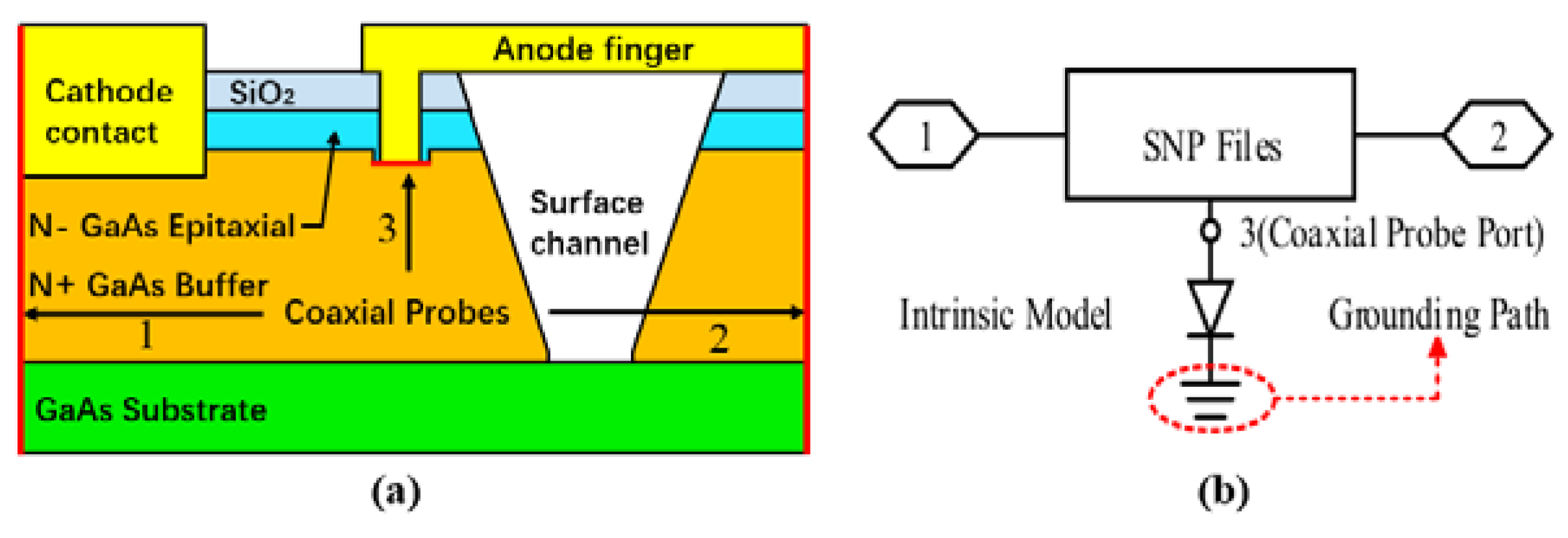
In the current terahertz frequency doubling circuit design, the commonly used diode model is a physics-based numerical model, also known as the 3-D EM model [
5]. The 3-D EM model utilizes a complete electromagnetic analysis method based on Maxwell’s equations to characterize the high-frequency parasitic effects caused by the complex passive structure around the Schottky junction. The diode SPICE model is used for characterizing the intrinsic nonlinear capacitance behavior of the diode. As shown in
Figure 1, a miniature coaxial probe is precisely inserted at each position of the Schottky junction, and a wave port is allocated at the end of the coaxial probe for connecting the diode SPICE model [
6,
7,
8]. The parasitic effects are imported in the form of a scatter matrix into the Agilent Advanced Design System (ADS) for further combining with the intrinsic model of a diode to predict the nonlinear capacitance behavior of the diode. This method has become a general modeling technique for SBDs and is widely used in the design of terahertz Schottky diode multipliers [
9,
10,
11,
12,
13,
14,
15], mixers [
16,
17,
18,
19], and detectors [
20,
21].
The electromagnetic model obtained through the method of complete electromagnetic analysis based on Maxwell’s equations could effectively characterize the high-frequency parasitic effects. Accurately obtaining the diode intrinsic nonlinear capacitance behavior is an important factor in the accuracy of the 3-D EM model. In the design of the terahertz hybrid integrated circuits, the zero-bias junction capacitance combined with the diode varactor formula is used for generating the varactor characteristics [
13,
15]. This method uses the variable capacitance formula under the DC condition, which cannot accurately characterize the C-V characteristics of the diode under high frequencies. In the process of Terahertz monolithic integrated circuit (TMIC) design, the C-V characteristics measured by the semiconductor parameter analyzer provide the data basis for obtaining the intrinsic nonlinear capacitance behavior of the diode [
22,
23]. The semiconductor parameter analyzer can only obtain the total capacitance of the diode structure along with the test structure and cannot accurately characterize the intrinsic junction capacitance of the diode.
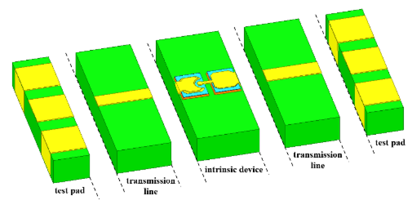
The physical size of the device is smaller than the value of accuracy of the on-chip test probe; thus, the test pads and the interconnects are required to access the device under test (DUT) (
Figure 2). In the small-signal S-parameter testing, these test pads and interconnects introduce additional effects. The measurement results cannot accurately characterize the small-signal characteristics of the device, although there are on-chip test de-embedding methods that could reduce the impact of the test results to a certain extent [
24,
25,
26]. As the frequency increases, the test pad and the transmission structure cannot simply be equivalent to the ground capacitance and ideal transmission line, respectively. This makes the errors of the parasitic effects from the test pad, and those of the interconnects, more prominent. An accurate de-embedding method is therefore required to eliminate these parasitic contributions.
In this paper, a new method is developed, named the Two-step Six-configuration Parameter Extraction Method (TSPEM). This method is divided into two parts: The peripheral structure de-embedding and parameter extraction. During the peripheral structure de-embedding step, the effect of the peripheral test structure is de-embedded by calculating the scattering matrix. In the parameter extraction step, the effect of the parasitic parameters of the diode is extracted and removed through four auxiliary configurations, and finally, the accurate value of the intrinsic junction capacitance is obtained. The TSPEM possesses the characteristics of high precision and simplicity, and it shows a better performance in de-embedding the contributions of the parasitic structures from the transmission line measurements and can extract the intrinsic junction capacitance value more accurately at a higher frequency. Later, the accuracy of the method was verified through electromagnetic simulation and the on-chip measurement results. A 180–220 GHz doubler was built to verify the accuracy of the model built using the TSPEM.
2. Methods
The TFPEM method aims to obtain the precise value of the junction capacitance at high frequencies by using the matrix de-embedding algorithm and the equivalent circuit parameter extraction method. The first step is to de-embed the test results at both ends of the device by two de-embedding auxiliary configurations. The second step is to accurately obtain the value of the junction capacitance by the four parameters of the extraction auxiliary configurations.
2.1. Peripheral Structure De-Embedding
This method realizes the de-embedding of the test results through the transmission matrix operation of the cascade system. It also reduces the impact error caused by the discontinuity when the test pads and transmission structure are directly equivalent to capacitors and an ideal transmission line.
Figure 2 reveals that the transmission matrix of either of the test structures can be decomposed into a cascade of five two-port networks. The network comprises test pads, the transmission lines and associated pad-line discontinuities, and the intrinsic device.
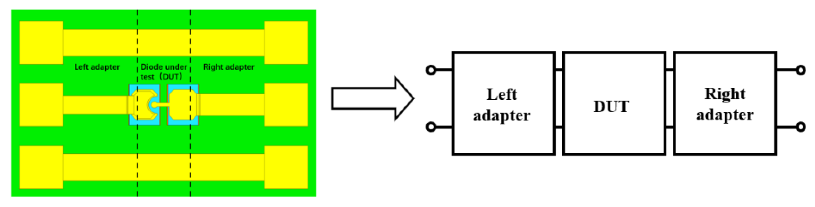
The pads and transmission lines can be concentrated in a single two-port network without losing generality. Equivalent representations of the test on-chip structure of the device are simplified, as shown in
Figure 3. Consequently, the (ABCD) transmission matrix of the test on-chip structure of the device can be represented by the following formula:
where
is a two-port network formed by the cascading left transmission line and the left pad. Left
is a two-port network formed by the cascading right transmission line and the right pad.
is a hybrid structure composed of the DUT and the electrical coupling between the left and right transmission structures.
can be expressed as:
Like the on-chip test, the open pad structure can also be expressed as:
and
can be obtained by de-embedding the auxiliary “pad-through” configuration. Since the interaction is very small, the direct interaction between the two transmission structures is not considered.
can be represented by two mirrored cascading T-shaped networks, as shown in
Figure 4. One single transmission structure is modeled as one shunt impedance and two series impedances, respectively.
can be expressed as:
Later, we have the transmission matrix of the two transmission structures:
The hybrid structure DUT’can be expressed in terms of the Y-parameters as a parallel combination of the DUT and the electrical coupling between the left and right transmission structures. The effects of electrical coupling can be canceled out, and the DUT can be expressed as:
2.2. Parasitic Research
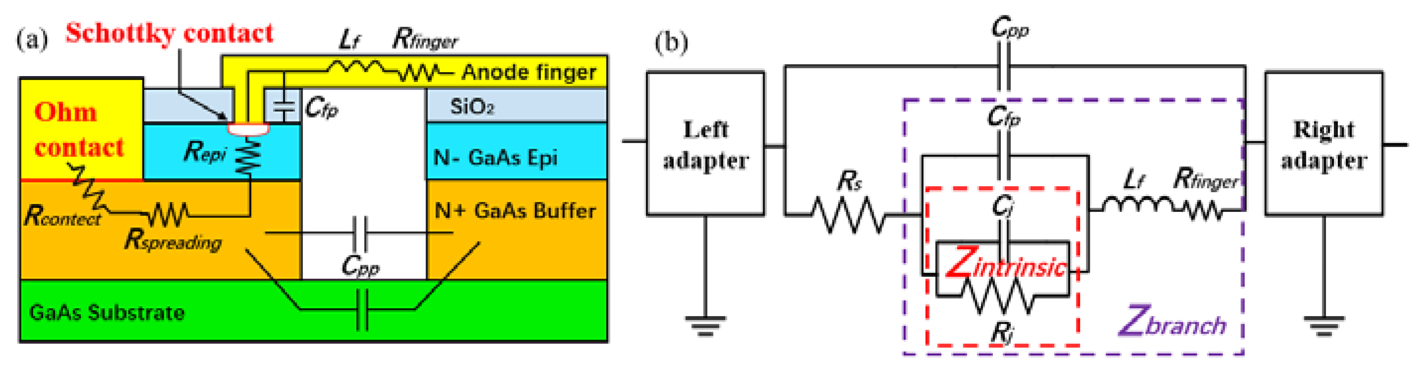
After obtaining the transfer matrix de-embedded to both ends of the device, the research process of the SBD parasitic characteristics is explained. The equivalent circuit was built based on the particular structure of the SBD. The coupling field between both pads and the finger-to-pad coupling are modeled as
Cpp and
Cfp. The air-bridge finger is modeled as self-inductance (
Lf) and the series resistance (
Rf) in the series structure. The equivalent circuit is shown in
Figure 5. The parasitic inductance of the cathode and anode two mesas L
pad << Lf, which can be neglected. Z
branch is the equivalent circuit of the diode metal finger and junction branch, which ignores the influence of mesa parasites. Z
intrinsic represents the intrinsic part of the diode, which is composed of intrinsic junction capacitance (
Cj) and junction resistance (
Rj) in parallel, where the junction capacitance can be described as:
where
is the edge effect correction factor,
ND is the doping concentration,
Vbi is the built-in potential difference, and
Aa is the junction area.
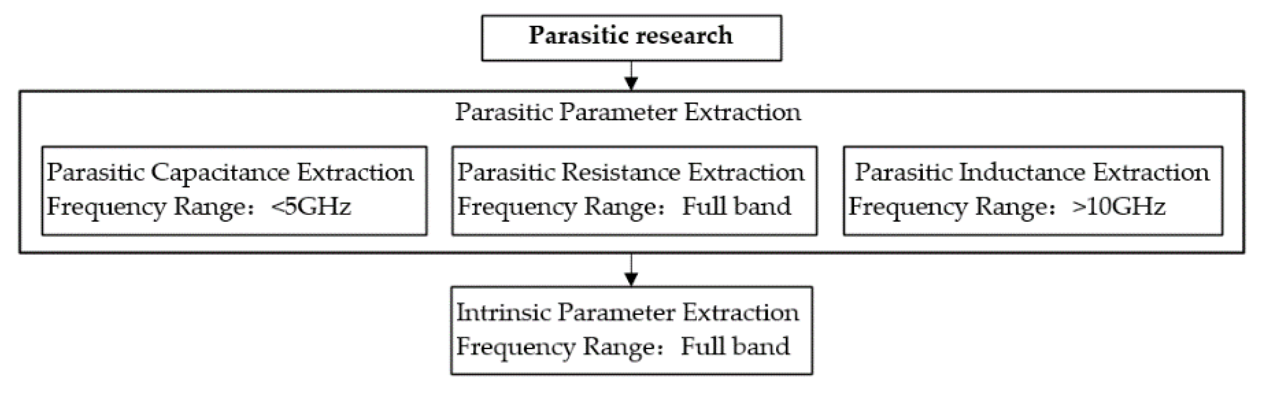
The value of these parasitic parameters can be found by the second step of the TFPEM method, and then, the value of the junction capacitance can be obtained. The possible steps for parameter research are shown in the flow diagram shown in
Figure 6. First, the value of the parasitic parameter is extracted through the four extraction configurations. Then, the value of the intrinsic junction capacitance is obtained by bringing the value of the parasitic parameter obtained into the equivalent circuit in
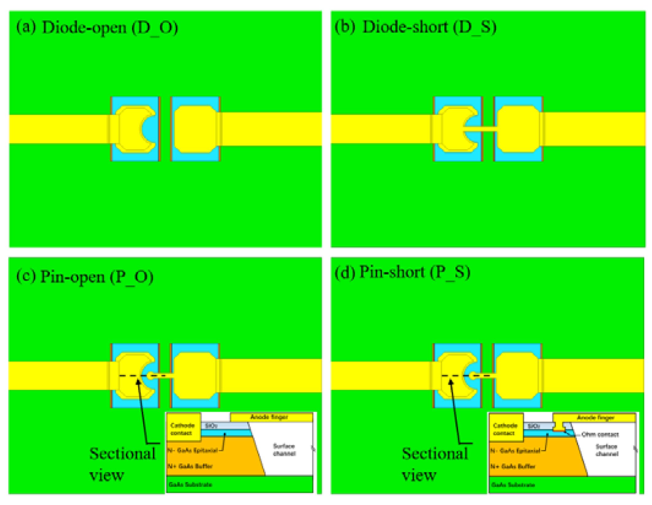
Figure 5b. In this step, four extraction configurations are used, namely, the diode-open, diode-short, pin-open, and pin-short. The detailed information of the configuration is illustrated by the corresponding simulation model, which is shown in
Figure 7. The diode-open structure is a diode structure without a metal finger. The diode-short structure is a diode structure in which the metal finger directly connects the cathode and the anode. The pin-open structure is a diode structure without Schottky contact. The pin-short structure is a diode structure in which ohmic contact is achieved at the Schottky junction through high work function metal and annealing.
2.2.1. Step 1—Parasitic Capacitance Extraction
The high-frequency electromagnetic coupling brought about by the diode geometry is mainly reflected in the parasitic capacitances. For a high-frequency planar diode, the capacitances range within a tenth to tens of a femtofarad. Thus, the parasitic capacitors are extracted at a relatively low-frequency range, e.g., the lower gigahertz frequency range. In this frequency band, the diode capacitances are dominant compared to parasitic inductances and resistances. With this, the influence of parasitic inductance and resistance can be neglected in the process of capacitor extraction. The diode
Cpp and
Cfp is estimated from the diode-open, pin-open, and extraction auxiliary configurations. Since the equivalent circuit is reciprocal, the parasitic capacitances are calculated as per the following assumptions (8) and (9).
2.2.2. Step 2—Parasitic Resistance Extraction
In general, the series resistance for a surface-channel planar Schottky diode is composed of an air-bridge finger resistance
Rfinger, top junction epi-layer resistance
Repi, buffer-layer spreading resistance
Rspreading, and ohmic-contact resistance
Rcontact. Among them, the
Repi,
Rspreading, and
Rcontact constitute the series resistor
Rs formed by the cathode mesa of the diode, as stated in (1). In this paper, an ideal conductor is assumed, and other series resistance components are ignored (i.e., treated as perfect electric conductors).
The diode resistance is calculated with pad-open, pad-short, and pin-short auxiliary configurations. Compared to the DC method, the resistance obtained by this method is more realistic under high-frequency conditions.
2.2.3. Step 3—Parasitic Inductance Extraction
The parasitic inductance of planar Schottky diodes is mainly derived from metal fingers. The inductance resides within the range of several to tens of pico-Henrys. In the traditional extraction method, the parasitic inductances are extracted at high frequencies, for instance, ranges of hundreds of gigahertz, which raises the requirements for the test system. Here, we use pad-open and pad-shirt auxiliary configurations to extract the value of the parasitic inductance.
2.2.4. Step 4 —Intrinsic Parameter Extraction
The junction capacitance of the planar Schottky diode comes from the space charge region formed by the Schottky contact. The capacitance-voltage (C-V) characteristics of the SBD can be measured by using the semiconductor parameter analyzer. However, the capacitance obtained by the measurement method is the total capacitance of the SBD. The total capacitance consists of the intrinsic junction capacitance (C
j), finger-to-pad capacitance (C
fp), and the pad-to-pad capacitance (C
pp). However, it cannot be simply expressed as the sum of capacitances. By bringing the parasitic parameters obtained in the first three steps into the model, as shown in
Figure 5b, and by eliminating their influence, the value of the SBD intrinsic junction capacitance can be obtained through parameter fitting through engineering. At the same time, the analytical expression of junction capacitance is also given. Its numerical calculation formula is provided as follows.
3. Results and Discussion
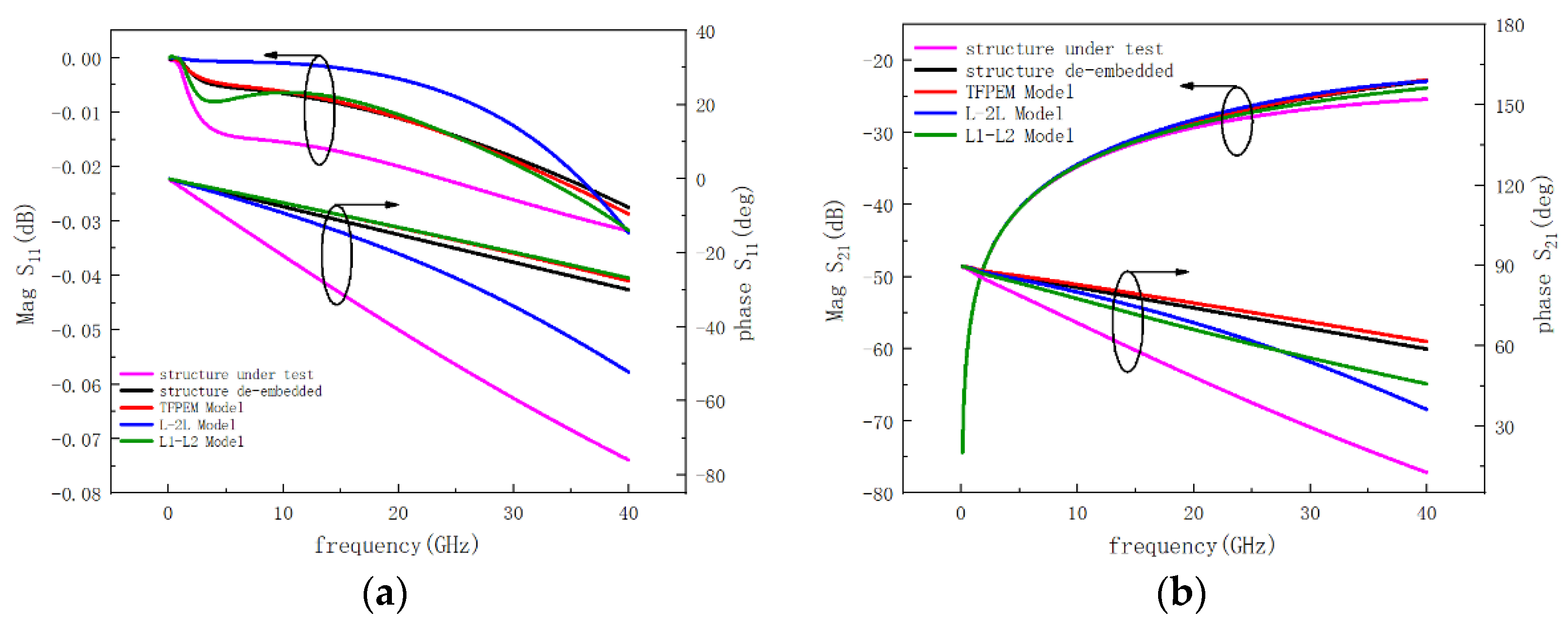
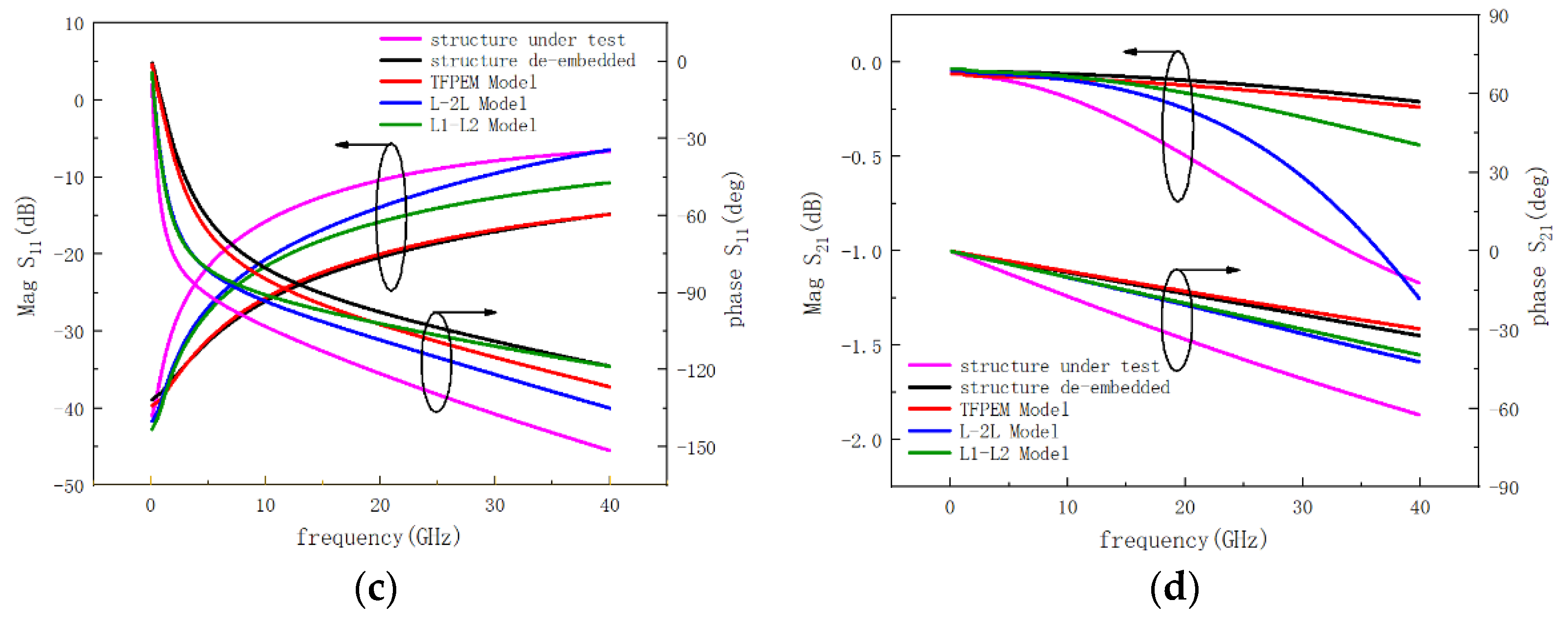
The effectiveness of this de-embedding method is verified through the three-dimensional electromagnetic simulation results, in which the 3-D electromagnetic models of the structure of the parameter extraction parts are built. The ports of the 3-D electromagnetic model are directly set on the edges of both sides of the anode and cathode. This model is used for accurately characterizing the electromagnetic characteristics of the parasitic parameter extraction structure. Three-dimensional models of the parasitic parameter extraction structure under test and the de-embedded structures are also built, in which the wave ports are set at the two edges of the CPW transmission structure, which is the same as the measurement structure. This model is used for simulating the result of the on-chip measurement of the parasitic parameter extraction structures and a de-embedded structure. The electromagnetic simulation results of the above structure in the 3-D electromagnetic simulation software are exported in the form of the S-parameter files. The electromagnetic characteristics of the parasitic test structure are de-embedded by the matrix operations.
Figure 8 shows the comparison between the S-parameters before and after the de-embedding of the parasitic test structures along with the S-parameters of the parasitic de-embedding structure. It can be seen that the de-embedding method mentioned in this paper is more accurate at higher frequencies compared to the other methods (L–2L method [
25], L1–L2 method [
26]). This de-embedding method can effectively remove the influence of the parasitic parameter caused by the test pads and the transmission line during the SBD parameter extraction process.
A series of GaAs SBD were produced with different Schottky junction diameters, de-embedding structures, and parasitic parameter extraction structures. The diameters of this series of diodes are 2 μm, 3 μm, 4 μm, and 5 μm. Apart from the Schottky junction diameter, the structure and physical dimensions of the SBD are the same in this series of diodes, which makes it have the same parasitic parameters but different junction capacitance values. Since the parasitic parameters do not change with the bias voltage, we tested the electromagnetic coupling characteristics of the de-embedding structures and the parasitic parameter extraction structures with the bias voltage (V
bias) = 0 V. The intrinsic junction capacitance (
Cj0) and the parasitic parameters included the pad-to-pad capacitance (
Cpp), finger-to-pad capacitance (
Cfp), finger inductance (
Lf), finger resistance (
Rf), and the cathode series resistance (
Rs). The extraction results of these parasitic parameters are shown in
Table 1. These parameters help better guide the design of the physical structure of the diode.
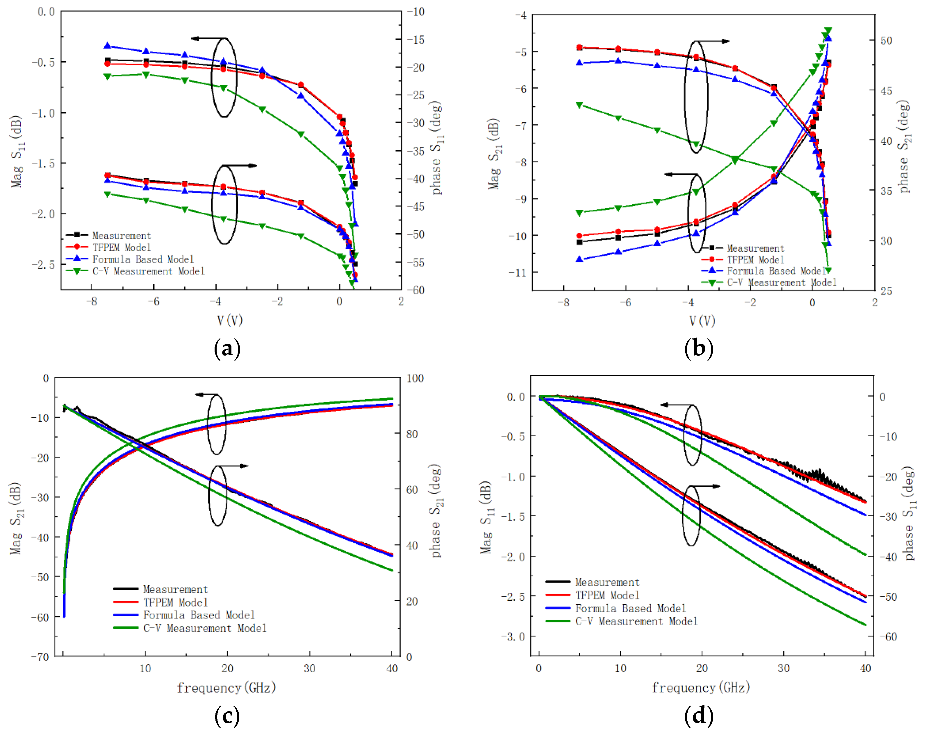
We bring the C-V characteristics obtained by three different junction capacitance extraction methods into the model shown in
Figure 1 to obtain a three-dimensional simulation model of the diode. In Method 1, the C-V characteristic of the diode junction capacitance is obtained through TFPEM. In Method 2, The C-V characteristic of the diode is measured by a semiconductor analyzer. In Method 3, the I-V test result of the diode is used to obtain the value of the thickness of the Schottky junction depletion layer, and then the junction capacitance is equivalent to the traditional formula of parallel plate capacitance to obtain the C-V characteristic of the diode as shown in Equation (7). The formula for the capacitance obtained in Method 3 is as follows.
Figure 9 shows the comparison between the electromagnetic characteristics of the three diode models and the measured results. It can be seen that the model established by the C-V characteristics obtained by the TFPEM showed very good consistency with the test results. The variable capacitance characteristics of the device are well characterized in the model. The model established by the C-V characteristics obtained by the semiconductor analyzer at a frequency of 1 MHz showed a greater coupling effect because the influence of the parasitic parameters was not eliminated. The model established by the I-V extraction method and the C-V characteristic obtained by the traditional formula [
27] showed a greater varactor characteristic because of the inability to correct the built-in voltage. The accuracy of this method is evaluated by computing the errors between the S-parameters for the device-under-test (DUT) and the extracted model. The frequency and voltage-dependent error function is written as:
where
and
are the measurement and three model S-parameters at different voltage points, respectively. The average error,
is defined as:
The average errors of the TFPEM model, the formula-based model, and the C-V measurement are 0.0011, 0.0173, and 0.1168, respectively. There is more remarkable agreement between the characteristics obtained by the method proposed in this paper and the measured results compared to other methods.
4. Application
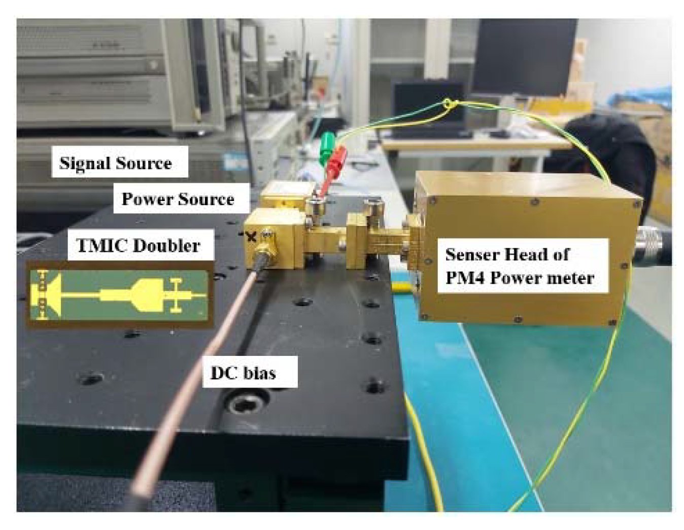
To further verify the accuracy of the model, a 200 GHz TMIC doubler circuit was simulated based on this model, and the simulation results were compared with the measured results for verification [
13]. The measurement was carried out under low-power conditions, eliminating the error caused by the increase in reverse leakage during high-power conditions. The cavity of the designed doubler was made of brass material, and the entire surface was gold-plated. The measurement setup employed for testing the frequency doubler MMICs is presented in
Figure 10. Here, an analog signal generator followed by a W-band, active × 8 frequency multiplier was utilized to generate an input signal in the 86–106 GHz band with a typical output power of +10 dBm. The output power of the frequency multipliers was measured using a PM4 power meter. In addition, a Sub-Miniature version A (SMA) coaxial RF connector was connected to the main transmission circuit using gold wire bonding, and a low forward bias (+0.8 V) was applied to the SMA port to bias the SBDs in the TMIC doubler.
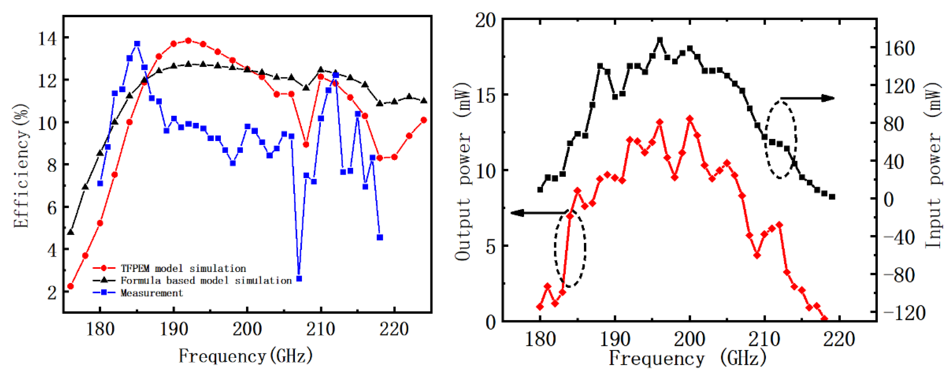
The TFPEM model simulation and the measured output power of the TMIC doubler are shown in
Figure 11, which concern the frequency along with the input power. The measured output power of the TMIC doubler was greater than 5.0 mW within the range of 188 GHz to 212 GHz, and the maximum output power was about 13.35 mW at 200 GHz. The efficiency of the TMIC doubler was greater than 8% within the range of 182 GHz to 218 GHz except for individual frequency, and the maximum efficiency was 12.6% at 185 GHz. The center frequency and bandwidth of the TFPEM model simulation results were consistent with the measurement results compared with the formula-based model simulation results. The minimum point around 207 GHz was better reflected in the TFPEM model simulation results. The difference in output power was mainly caused due to the introduction of resistance during assembly.
5. Conclusions
In this paper, the TSPEM method was developed to get a more accurate intrinsic junction capacitance value of the SBD in the Terahertz band. In the peripheral structure de-embedding step, the effect of the peripheral test structure is de-embedded by calculating the scattering matrix. In the parameter extraction step, the effect of the diode parasitic parameters is extracted and removed through four auxiliary configurations, and finally, the accurate value of the intrinsic junction capacitance is obtained. The accuracy of the de-embedding step and parameter extraction step of the TFPEM method was evaluated through three-dimensional electromagnetic simulation and diode on-chip measurement, respectively. The accuracy of this method was further verified by the performance of a 200 GHz double frequency converter. This method shows more accurate high-frequency characteristics and provides a more accurate simulation model for the future designs of the TMIC circuit.
Author Contributions
Formal analysis, X.L.; Investigation, B.W.; Methodology, X.L., H.W. and W.D.; Project administration, J.Z.; Software, X.L.; Visualization, L.Q.; Writing—original draft, X.L., Y.Z., Z.J. and F.X. All authors have read and agreed to the published version of the manuscript.
Funding
This research was funded by National Natural Science Foundation of China, grant number 61871072.
Conflicts of Interest
The authors declare no conflict of interest.
References
- Dhillon, S.S.; Vitiello, M.S.; Linfield, E.H.; Davies, A.G.; Hoffmann, M.C.; Booske, J.; Paoloni, C.; Gensch, M.; Weightman, P.; Williams, G.P.; et al. The 2017 terahertz science and technology roadmap. J. Phys. D Appl. Phys. 2017, 50. [Google Scholar] [CrossRef]
- Siegel, P.H. Terahertz Technology. IEEE Trans. Microw. Theory Tech. 2002, 50, 910–928. [Google Scholar] [CrossRef]
- Mehdi, I.; Siles, J.V.; Lee, C.; Schlecht, E. THz Diode Technology: Status, Prospects, and Applications. Proc. IEEE. 2017, 105, 990–1007. [Google Scholar] [CrossRef]
- Crowe, T.W.; Bishop, W.L.; Porterfield, D.W.; Hesler, J.L.; Weikle, R.M. Opening the terahertz window with integrated diode circuits. IEEE J. Solid State Circuits 2005, 40, 2104–2110. [Google Scholar] [CrossRef]
- Siles, J.V.; Grajal, J. Physics-Based Design and Optimization of Schottky Diode Frequency Multipliers for Terahertz Applications. IEEE Trans. Microw. Theory Tech. 2010, 58, 1933–1942. [Google Scholar] [CrossRef]
- Hesler, J.L.; Hall, W.R. Fixed-Tuned Submillimeter Wavelength Waveguide Mixers Using Planar Schottky-Barrier Diodes. IEEE Trans. Microw. Theory Tech. 1997, 45, 653–658. [Google Scholar] [CrossRef]
- Song, H.J.; Nagatsuma, T. Handbook of Terahertz Technologies: Devices and Applications; Kangogaku Zasshi; CRC Press: Boca Raton, FL, USA, 2015; pp. 101–131. [Google Scholar]
- Hesler, J.L. Planar Schottky Diodes in Submillimeter-Wavelength Waveguide Receivers. Ph.D. Dissertation, University of Virginia, Charlottesville, VA, USA, January 1996. [Google Scholar]
- Zhang, Y.; Zhong, W.; Ren, T.; Chen, Y.; Yan, B.; Xu, R. A 220 GHz frequency tripler based on 3D electromagnetic model of the schottky diode and the field circuit co-simulation method. Microw. Opt. Technol. Lett. 2016, 58, 1647–1651. [Google Scholar] [CrossRef]
- Wu, C.; Zhang, Y.; Cui, J.; Li, Y.; Xu, Y.; Xu, R. A 135-190 GHz Broadband Self-Biased Frequency Doubler using Four-Anode Schottky Diodes. Micromachines 2019, 10, 277. [Google Scholar] [CrossRef] [PubMed] [Green Version]
- Jiang, J.; Lu, B.; Miao, L.; He, Y.; Shi, X.; Tian, Y.; Hao, H.; Chen, F.; Deng, X.; Zhang, J. Single-Stage Frequency Quadrupler With SBD and Four-Octave LPF at 335 GHz. IEEE Trans. Terahertz Sci. Technol. 2017, 7, 446–454. [Google Scholar] [CrossRef]
- Yan, B.; Ren, T.; Wu, C.; Wei, H.; Wang, L.; Li, Y.; Xu, R.; Zhang, Y. A 140 GHz high efficiency frequency doubler based on a physical-based SDD model of SBD. Int. J. Circuit Theory Appl. 2021, 49, 1378–1389. [Google Scholar] [CrossRef]
- Qi, L.; Meng, J.; Liu, X.; Yang, C.; Zhou, J.; Zhang, D.; Jin, Z. Design of a Schottky Metal-Brim Structure to Optimize 180–220 GHz Broadband Frequency Doubler MMIC. Electronics 2020, 9, 715. [Google Scholar] [CrossRef]
- Meng, J.; Qi, L.; Liu, X.; Zhou, J.; Zhang, D.; Jin, Z. The Design of Terahertz Monolithic Integrated Frequency Multipliers Based on Gallium Arsenide Material. Micromachines 2020, 11, 336. [Google Scholar] [CrossRef] [PubMed] [Green Version]
- Doo, J.; Kim, J.; Jeong, J. D-Band Frequency Tripler Module Using Anti-Parallel Diode Pair and Waveguide Transitions. Electronics 2020, 9, 1201. [Google Scholar] [CrossRef]
- Zhang, B.; Zhang, Y.; Pan, L.; Li, Y.; Cui, J.; Xu, R.; Yan, B. A 560 GHz Sub-Harmonic Mixer Using Half-Global Design Method. Electronics 2021, 10, 234. [Google Scholar] [CrossRef]
- Guo, C.; Shang, X.; Lancaster, M.J.; Xu, J.; Powell, J.; Wang, H.; Parow-Souchon, K.; Henry, M.; Viegas, C.; Alderman, B.; et al. A 290–310 GHz Single Sideband Mixer With Integrated Waveguide Filters. IEEE Trans. Terahertz Sci. Technol. 2018, 8, 446–454. [Google Scholar] [CrossRef] [Green Version]
- He, Y.; Tian, Y.; Miao, L.; Jiang, J.; Deng, X.J. A Broadband 630-720 GHz Schottky Based Sub-Harmonic Mixer Using Intrinsic Resonances of Hammer-Head Filter. China Commun. 2019, 16, 76–84. [Google Scholar]
- Ji, D.; Zhang, B.; Yang, Y.; Niu, Z.; Chen, X. A 220-GHz Third-Harmonic Mixer Based on Balanced Structure and Hybrid Transmission Line. IEEE Access 2019, 7, 50007–50011. [Google Scholar] [CrossRef]
- Schiselski, M.; Laabs, M.; Neumann, N.; Kovalev, S.; Plettemeier, D. A planar Schottky diode based integrated THz detector for fast electron pulse diagnostics. In Proceedings of the 2016 IEEE MTT-S International Microwave Symposium (IMS), San Francisco, CA, USA, 22–27 May 2016. [Google Scholar]
- Ederra, I.; Gonzalo, R.; Martinez, B.; Alderman, B.E.J. Design and Test of a 0.5 THz Dipole Antenna With Integrated Schottky Diode Detector on a High Dielectric Constant Ceramic Electromagnetic Bandgap Substrate. IEEE Trans. Terahertz Sci. Technol. 2013, 3, 584–593. [Google Scholar] [CrossRef]
- Zhang, B.; Ji, D.; Fang, D.; Liang, S.; Fan, Y.; Chen, X. A Novel 220-GHz GaN Diode On-Chip Tripler With High Driven Power. IEEE Electron Device Lett. 2019, 40, 780–783. [Google Scholar] [CrossRef]
- Liang, S.; Song, X.; Zhang, L.; Lv, Y.; Wang, Y.; Wei, B.; Guo, Y.; Wang, B.; Cai, S.; Feng, Z. A 177–183 GHz High-Power GaN-Based Frequency Doubler With Over 200 mW Output Power. IEEE Electron Device Lett. 2020, 41, 669–672. [Google Scholar] [CrossRef]
- Tiemeijer, L.F.; Havens, R.J. A calibrated lumped-element de-embedding technique for on-wafer RF characterization of high-quality inductors and high-speed transistors. IEEE Trans. Electron Devices 2003, 50, 822–829. [Google Scholar] [CrossRef]
- Bu, Q.; Li, N.; Okada, K.; Matsuzawa, A. Evaluation of L-2L De-Embedding Method Considering Misalignment of Contact Position for Millimeter-Wave CMOS Circuit Design. IEICE Trans. Electron. 2012, 95, 942–948. [Google Scholar] [CrossRef]
- Mangan, A.M.; Voinigescu, S.P.; Yang, M.T.; Tazlauanu, M. De-embedding transmission line measurements for accurate modeling of IC designs. IEEE Trans. Electron Devices 2006, 53, 235–241. [Google Scholar] [CrossRef] [Green Version]
- Maestrini, A.; Thomas, B.; Hui, W.; Jung, C.; Treuttel, J.; Jin, Y.; Chattopadhyay, G.; Mehdi, I.; Beaudin, G. Schottky diode-based terahertz frequency multipliers and mixers. Comptes Rendus Phys. 2010, 11, 480–495. [Google Scholar] [CrossRef]
| Publisher’s Note: MDPI stays neutral with regard to jurisdictional claims in published maps and institutional affiliations. |
© 2021 by the authors. Licensee MDPI, Basel, Switzerland. This article is an open access article distributed under the terms and conditions of the Creative Commons Attribution (CC BY) license (https://creativecommons.org/licenses/by/4.0/).


 ,
, 


