Production Methods of Van der Waals Heterostructures Based on Transition Metal Dichalcogenides

1
Shaanxi Engineering Lab for Advanced Energy Technology, School of Materials Science and Engineering, Shaanxi Normal University, Xi’an 710119, China
2
School of Materials Science and Engineering, Nanyang Technological University, Singapore 639798, Singapore
*
Authors to whom correspondence should be addressed.
Crystals 2018, 8(1), 35; https://doi.org/10.3390/cryst8010035
Submission received: 14 November 2017
/
Revised: 11 January 2018
/
Accepted: 11 January 2018
/
Published: 15 January 2018
(This article belongs to the Special Issue Two-Dimensional Materials beyond Graphene and their Van der Waals Heterostructures)
Abstract
:Two dimensional (2D) materials have gained significant attention since the discovery of graphene in 2004. Layered transition metal dichalcogenides (TMDs) have become the focus of 2D materials in recent years due to their wide range of chemical compositions and a variety of properties. These TMDs layers can be artificially integrated with other layered materials into a monolayer (lateral) or a multilayer stack (vertical) heterostructures. The resulting heterostructures provide new properties and applications beyond their component 2D atomic crystals and many exciting experimental results have been reported during the past few years. In this review, we present the various synthesis methods (mechanical exfoliation, physical vapor transport, chemical vapor deposition, and molecular beam epitaxy method) on van der Waals heterostructures based on different TMDs as well as an outlook for future research.
1. Introduction
The family of two-dimensional (2D) materials has grown appreciably since the first isolation of graphene [1,2,3,4,5,6]. 2D materials usually have some unique properties that are very different from those of their 3D counterparts. During the past decades, more and more 2D materials have been reported [7,8,9,10,11,12,13] and offered a broad range of electronic properties from insulating (e.g., hexagonal boron nitride (h-BN)) or semiconducting (e.g., MoS2, WSe2) to semi-metallic (e.g., PtSe2, TiS2) or metallic (e.g., NbSe2), even superconducting (e.g., NbS2). This diversity offers the opportunity to construct atomically thin electronics based entirely on 2D materials [14,15,16]. Van der Waals heterostructures (combining several 2D layers by van der Waal forces) have been an attracting topic for both fundamental research and applied physics [17,18,19,20,21,22,23,24,25,26]. In 2010, Dean et al. reported the first heterostructures based on 2D materials, in which graphene was placed on top of thin h-BN layers [27]. In this heterostructures, graphene exhibits that the mobilities are almost an order of magnitude better than on SiO2. As the family of 2D materials is increasing gradually in recent years, this kind of heterostructures allows a greater freedom and a far greater number of combinations than any traditional growth method. Furthermore, van der Waals heterostructures have already led to the observation of numerous exciting physical phenomena and novel applications such as correlated light emitters [28,29,30,31], ultra-high speed photodetectors [32,33], new generation field effect transistors [34,35,36,37], and memory devices [38,39,40,41] compared to their individuals. Therefore, the investigation of van der Waals heterostructures shows great importance. In 2013, Geim et al. explained the significance of 2D heterostructures and proposed some possible directions in this area [42]. The most significant challenge to realize applications for these van der Waals heterostructures is the scalable synthesis of large-area and high-quality heterostructures. Even though the controlled growth of van der Waals heterostructures has gained increasingly attention [28,43,44,45,46,47,48], it is still an interesting and important topic in the future.
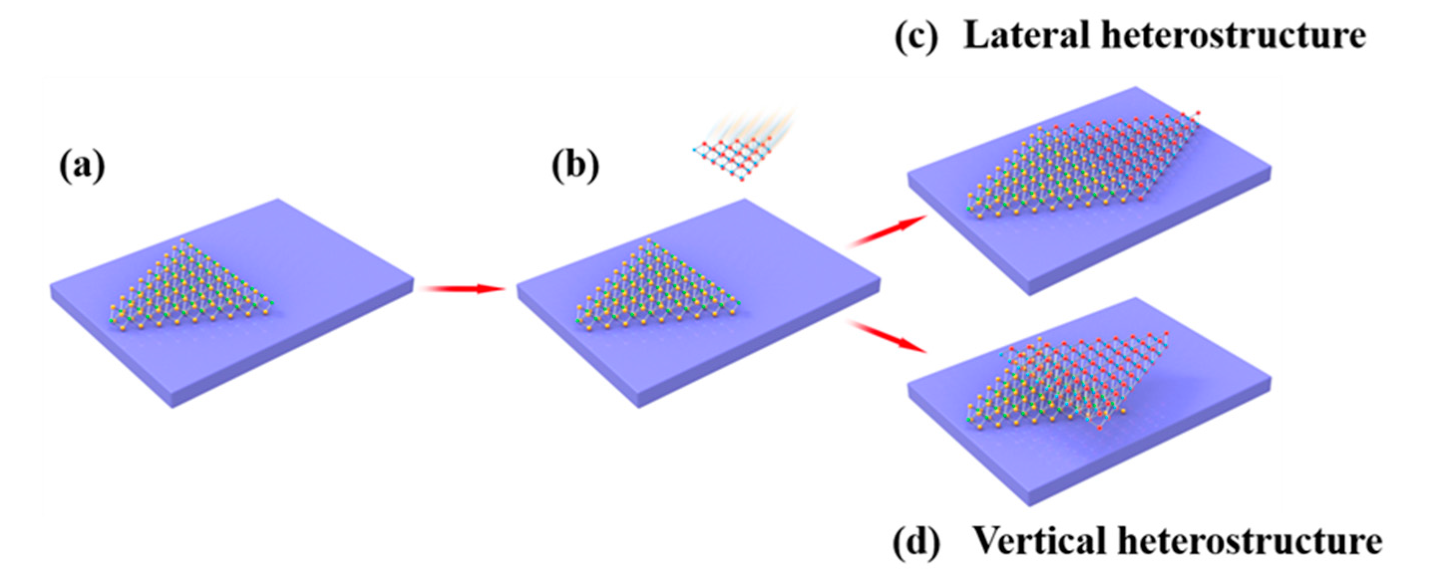
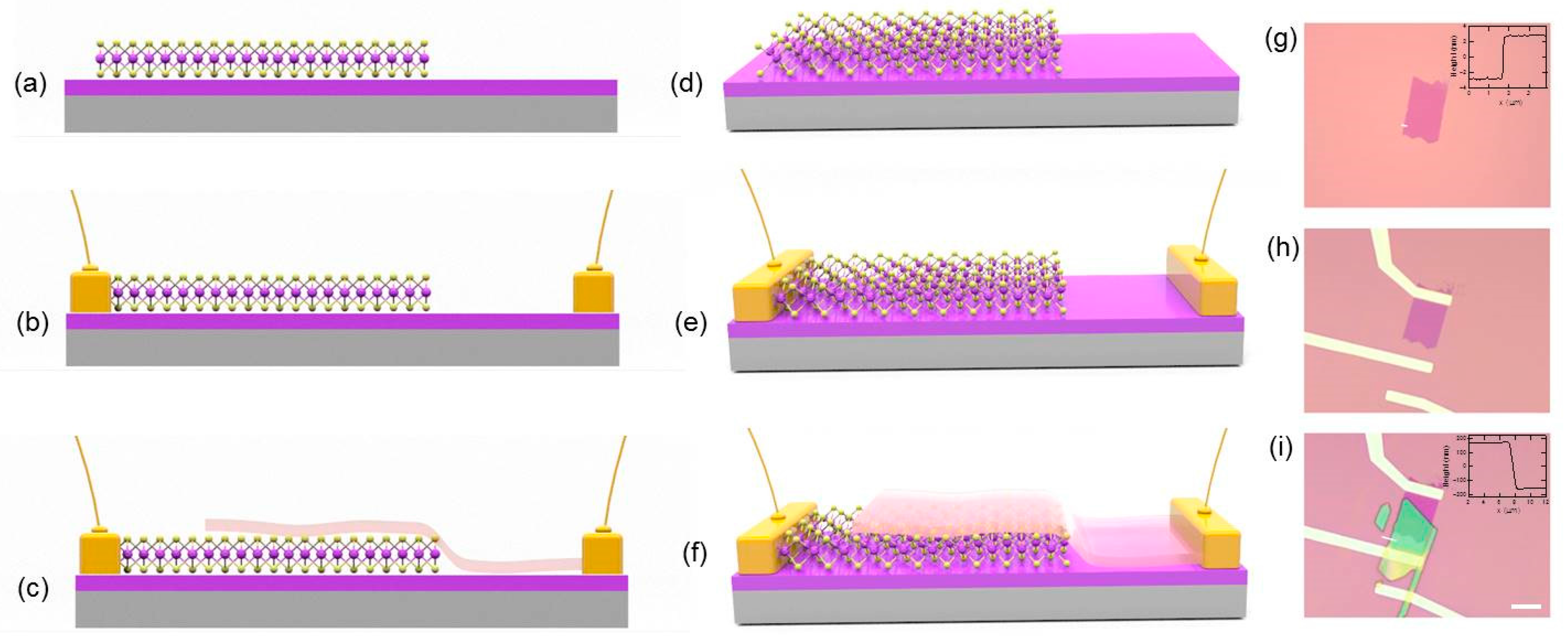
There are two strategies for obtaining heterostructures. One is assembling the different layers in a plane to form lateral heterostructures (Figure 1c) and another is vertically stacking different layered materials layer-by-layer (vertical heterostructure, Figure 1d). Figure 1 is the schematic illustration of the preparation of heterostructures. In a typical synthesis method, one layer of 2D materials is firstly put on the substrates (Figure 1a). Next procedure (Figure 1b) is growing or transferring another layered material to the first layer, which is the key step. If the two layers are connected in-plane (Figure 1c), they will form lateral heterostructures. If one layer is stacking onto another layer, vertical heterostructure will be constructed (Figure 1d).
For individual 2D materials, exfoliation techniques and chemical vapor deposition (CVD) are the most used technique. These two techniques are still the most popular methods for heterostructures based on TMDs. Compared to the physical method, CVD has shown its advance in the direct growth of 2D heterostructures. More importantly, this route could lead to the formation of heterostructures consisting of lattice aligned TMDs layers for both vertical and lateral cases. In addition, physical vapor transport/deposition (PVT/PVD) and molecular beam epitaxy (MBE) method are also used to grow TMDs heterostructures. In this review, we emphasize on various type of synthesis method on van der Waals heterostructures based on the most popular branch of 2D materials-TMDs.
2. Mechanical Exfoliation Method
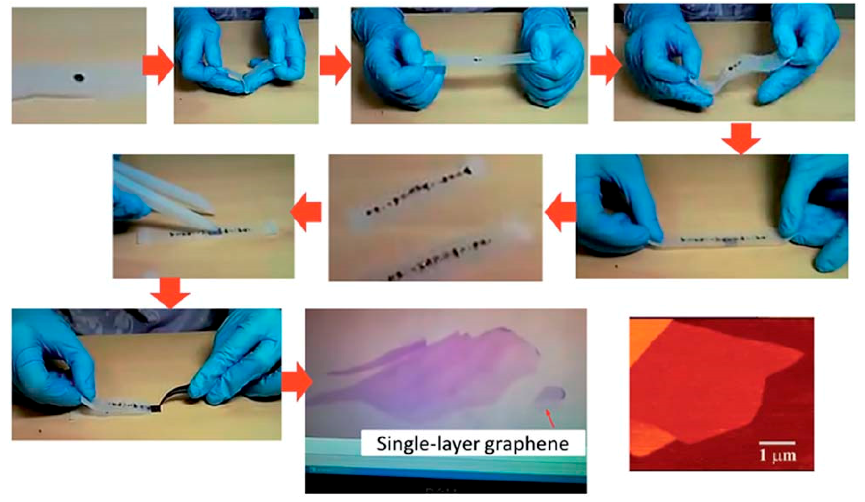
Mechanical exfoliation is the most widely used technique to synthesize ultraclean 2D-TMDs with variable thicknesses down to a single lattice unit [49]. Various kinds of 2D materials can be prepared on different substrates by mechanical exfoliation. Thus, such 2D samples can be stacked layer by layer to obtain vertical heterostructures [50]. In this process, Scotch tape [1] was used to produce flakes of 2D materials, which can overcome the van der Waals interaction between each layer. After that, such flakes of 2D materials can be transferred onto different substrates, such as quartz, SiO2/Si, polydimethylsiloxane (PDMS), etc. Then, one monolayer flake is precisely transferred onto another flake to obtain heterostructures under a microscope. Figure 2 shows a typical procedure of the Scotch-tape based micromechanical cleavage method of graphene [51]. The methods are also employed to other 2D materials, such as TMDs, black phosphorus (BP), etc.
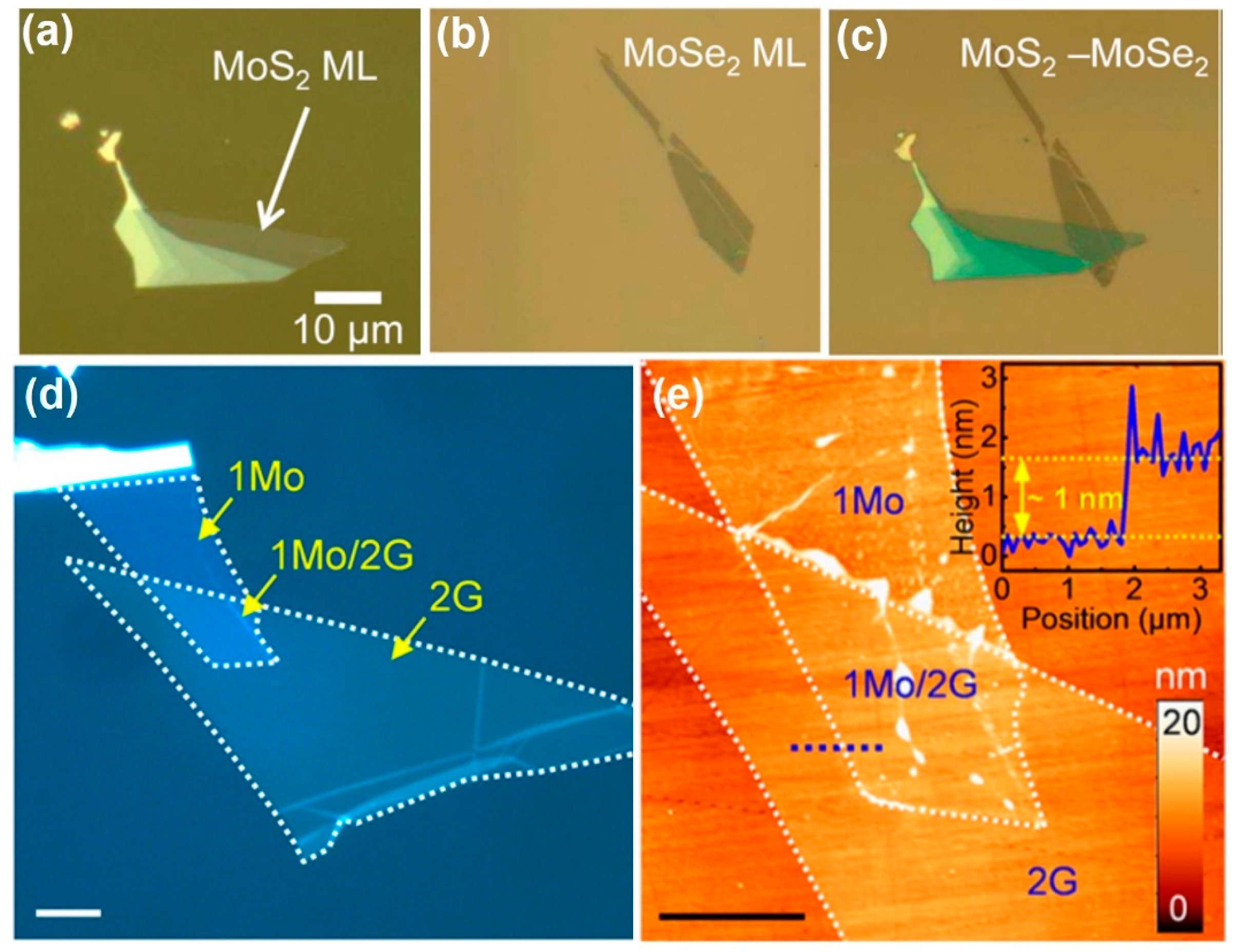
To probe interlayer interactions in transition metal dichalcogenide heterostructures [52], Rigosi’s group [53] successfully prepared the MoS2–WS2 and MoSe2–WSe2 heterostructures, respectively, by simply exfoliating the relevant crystals and then constructing the heterostructures by using mechanical transfer technique. In another case, to explore the interlayer exciton dynamics in a dichalcogenide monolayer heterostructure, MoSe2–WSe2 heterostructures were prepared by exfoliation of MoSe2 and WSe2 flakes from their bulk counterparts followed by a transfer process [54]. Furthermore, the preparation of high quality MoS2–MoSe2 [55] (Figure 3a–c), MoSe2–WS2 [56], WSe2–SnSe2 [57], and MoS2–WSe2 [58,59] was achieved by this method as well. Shi et al. [60] reported the fabrication of SiC with WSe2 surface flakes whose thickness ranged from several layers to several microns by this method and further studied the effects of energetic ion irradiation on such heterostructure. Lopez-Sanchez et al. [61] showed the realization of electroluminescent devices and solar cells based on vertical heterojunctions composed of n-type monolayer MoS2 and p-type silicon. Britnell et al. [62] first successfully obtained WS2–graphene heterojunction by combining the mechanical exfoliation and dry transfer method. MoS2–graphene heterostructures are also obtained by using the similar procedure by transferring MoS2 onto the graphene surface (Figure 3d,e) [63]. By using the same strategy, Moriya et al. [64] fabricated the graphene–MoS2–metal vertical field effect transistor, which showed superior electrical performance when compared with those of other graphene based vertical transistors.
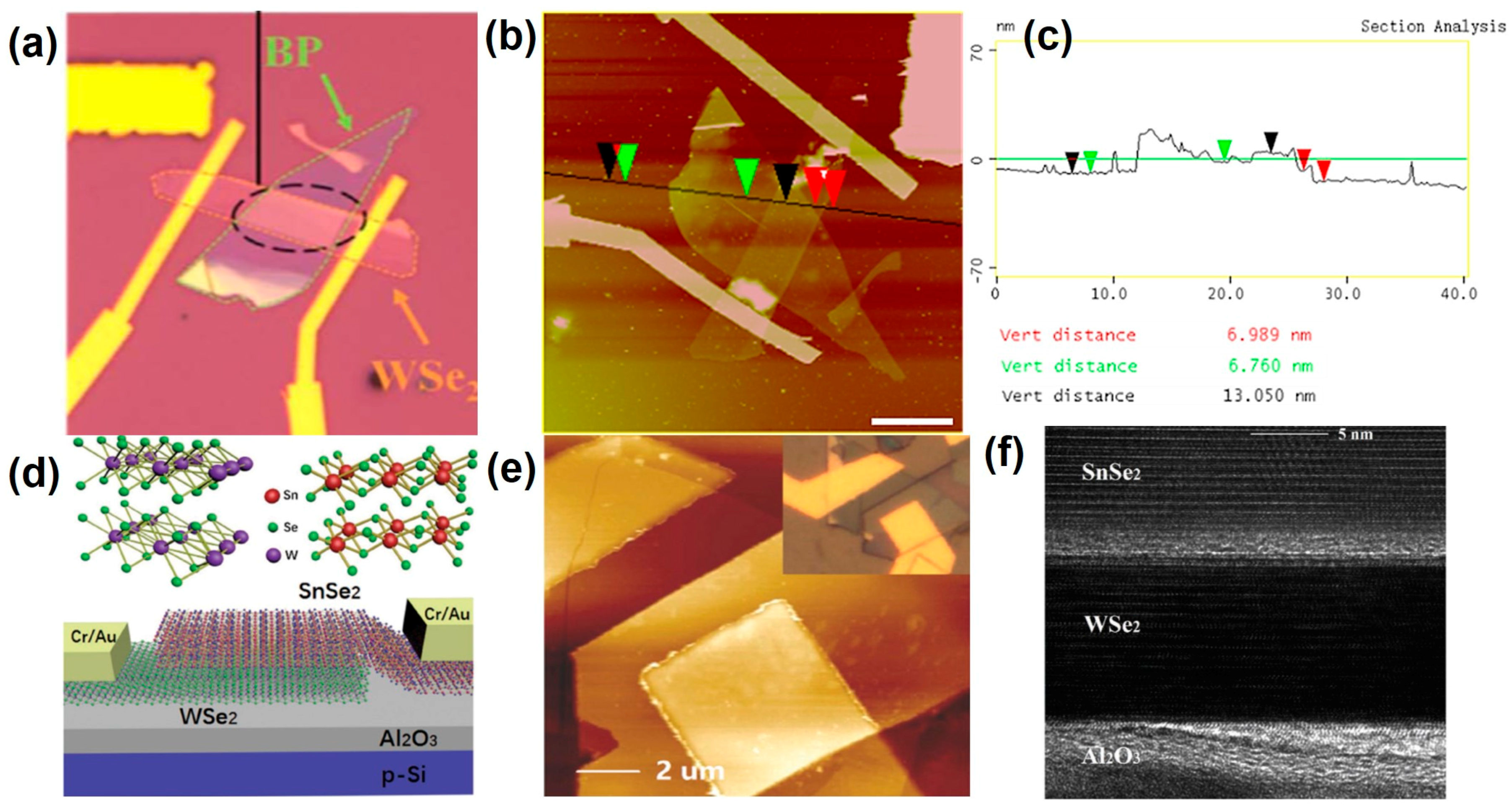
A novel mechanical exfoliation method, so-called “random transfer”, was proposed by Chen’s group to fabricate vertical heterostructures [65]. The few-layer BP and WSe2 were both mechanically exfoliated from bulk counterparts (Figure 4a–c). Furthermore, SnSe2–WSe2 heterostructures were obtained by using the same method (Figure 4d–f) [66]. The cross-sectional TEM image confirmed the heterostructures and a thin barrier (~1.8 nm) at the interface between SnSe2 and WSe2 is formed.
The mechanical exfoliation can also be applied to organic-inorganic heterostructures [37,68,69]. Liu et al. [70] reported an organic-inorganic heterostructure based on p-type organic rubrene single crystal and n-type 2D MoS2 (Figure 5). They fabricated FET devices based on MoS2–rubrene inorganic-organic heterostructures. MoS2 thin flakes were prepared by mechanical exfoliation on the Si wafer (Figure 5a,d,g). Then, gold electrode is evaporated thermally on top of MoS2 flake. Only one electrode was contacted to MoS2 flakes, and another was left empty (Figure 5b,e,h). After that, one side of rubrene single crystal was laminated on the fabricated gold electrode, and another side contacted with MoS2 flakes, forming bottom contacts and bottom gate geometry (Figure 5c,f,i). The as-prepared devices showed good photoresponse properties with a photoresponsivity of ~500 mA W−1 and a fast response time. These findings open up a new route to facilitate optoelectronic devices based on layered 2D inorganics and organic crystals.
3. Physical Vapor Transport/Deposition (PVT/PVD) Method
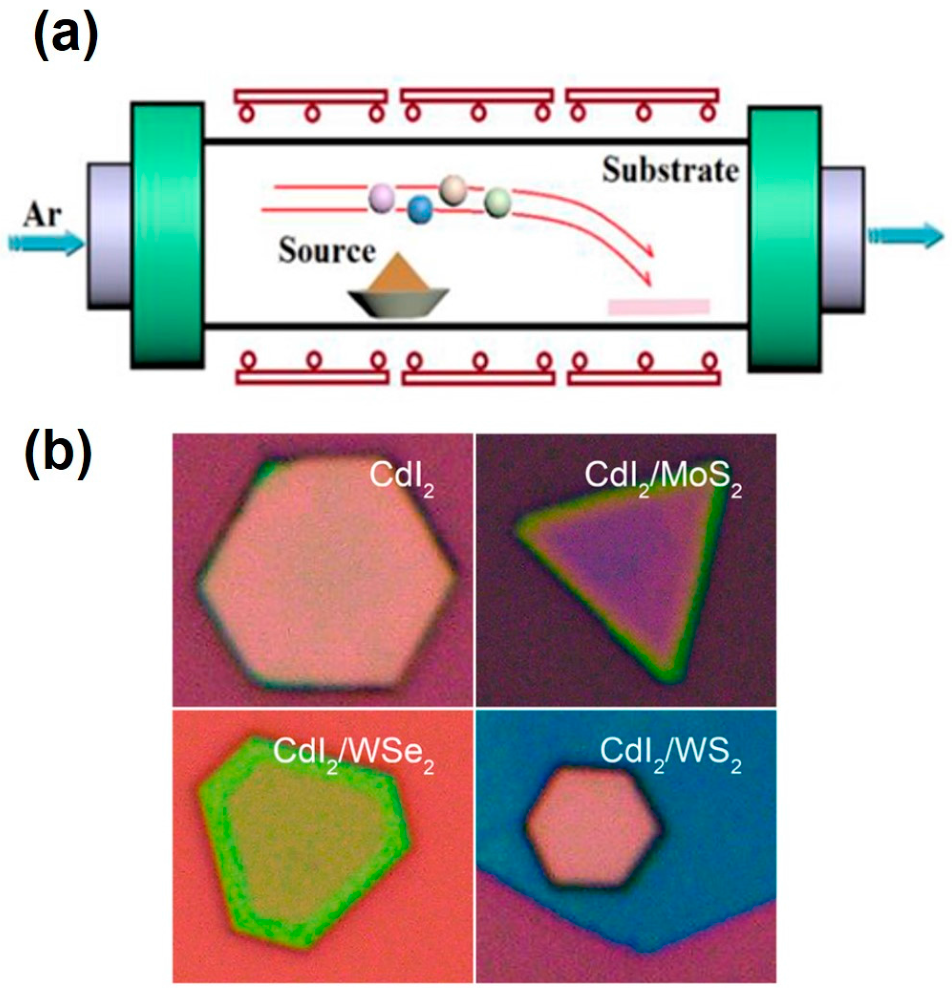
PVD and PVT methods are also used for synthesis TMDs-based heterostructures. Zhang et al. developed a high-quality topological crystalline insulator (TCI) SnTe film–Si vertical heterostructure by the growth of TCI SnTe film on Si substrate using a simple physical vapor deposition process (Figure 6a) [71]. High-purity SnTe powder was used as the precursor for evaporation. Different thickness of the SnTe films could be obtained by tuning the deposition time. The resultant heterostructure exhibits an obvious diode characteristic with a higher rectification ratio, which enables the fabrication of high-performance and self-driven photodetectors capable of broadband detection of near-infrared lights. Moreover, the successful synthesis of multiple-component heterostructures, (SnSe)1.16(MoSe2)1.06(SnSe)1.16(NbSe2)1, was achieved by carefully designed modulated precursors obtained by using a custom-built PVD system [72]. Ai et al. showed the ready growth of CdI2 nanoplates on other 2D TMDs (e.g., WS2, WSe2, MoS2) and the successful synthesis of regular arrays of CdI2–TMD van der Waals heterostructures by a two-step PVD strategy (Figure 6b) [73]. The as-grown 2D-TMDs nanosheets were used as the substrate for the van der Waals epitaxial growth of CdI2 nanoplates to obtain target heterostructures. The axial heterostructure nanowires consisted of ZnTe and Bi4Te3 segments which had an interesting fletching shape with three wings surrounded by ZnO shells. Furthermore, the two-dimensional CdS–CdSe lateral heterostructure nanobelts with a central CdSe region and lateral CdS structures can be also prepared via a two-step PVT method [74].
4. Chemical Vapor Deposition (CVD) Method
CVD, one of the most promising methods to grow high-quality 2D materials, can be adapted to create large-area heterostructures. It has proven to be the most effective technique to synthesize both vertical and lateral heterostructures [11,75]. The relative high-quality 2D material could be grown on surfaces with a well-controlled lateral size and layer thickness, which is well suited for device fabrications [49]. By directly growing one kind of material onto the surface of another, vertical heterostructures could be obtained. The surface defects will be significantly reduced if the surface of one-layer 2D materials has no dangling bonds. Thus, when forming vertical heterostructures, a clean interface between two different 2D materials can be realized [50].
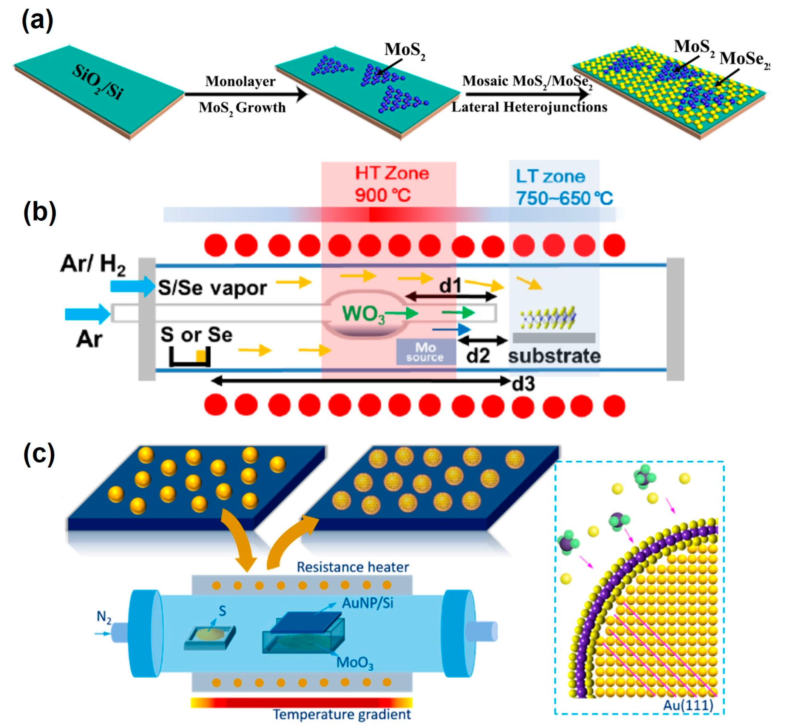
Many researchers investigated diverse types of TMDs-based heterostructures grown by CVD technique. Among all the kinds, TMDs–TMDs heterostructures are the most extensively studied. Ajayan’s group firstly developed one-step CVD to obtain WS2–MoS2 lateral and vertical heterostructures [22]. MoS2–MoSe2 lateral heterostructure film was successfully grown on SiO2/Si substrate for the first time using a two-step CVD technique by Chen’s group (Figure 7a) [76]. Triangular MoS2 monolayers were firstly grown on SiO2/Si substrate. Then, in the second CVD step, large-area MoSe2 film is merged with triangular MoS2 monolayers formed in the first step, generating a continuous mosaic MoS2–MoSe2 lateral heterostructures membrane. Furthermore, Zhang et al. [77] achieved a direct synthesis of monolayer MoS2–WS2 and MoSe2–WSe2 lateral heterostructures (Figure 7b). Sulfur and Se powders were placed in the crucible upstream and heated with a temperature of 200 and 300 °C, respectively. The WO3 powders were filled in the homemade quartz reactor and placed in the HT zone of the furnace. The WO3 vapor directly flows to the LT zone, which can be reacted with S/Se. By carefully adjusting the quantities of reactants and the distance between source and substrate, lateral heterostructures with different TMD atomic layers could be obtained. Additionally, by using a one-step and facile CVD method, Jung et al. [78] prepared MoS2–WS2 and MoSe2–WSe2 heterostructures that owned vertically aligned 2D layers with well-defined structures and compositions over a large area. First, SiO2/Si substrates were deposited with lithographically patterned Mo/W thin films. Subsequently, the Mo/W films converted into homologous TMDs by reacting with sulfur (selenium) via a CVD process. The heterostructures can be obtained after 15 min growth. Li et al. [79] designed Au@MoS2 core-shell heterostructures that were synthesized by direct growth of multilayer fullerene-like MoS2 shell on Au nanoparticle cores (Figure 7c). During deposition, volatile MoO3 and its partially decomposed suboxides react with sulfur vapor to form a MoS2 shell on the Au nanoparticles. In another example, a novel 2D–3D Ge–MoS2 heterostructure consisted of single crystalline Ge (110) thin film and monolayer MoS2 was prepared via low-pressure CVD [80]. The growth of ZnCdSSe quaternary alloy heterostructures was obtained by this method as well [81]. CdSe and ZnS powders were used as source materials and placed into the high-temperature zone. The final heterostructures can be obtained by controlling the growth time and substrate position.
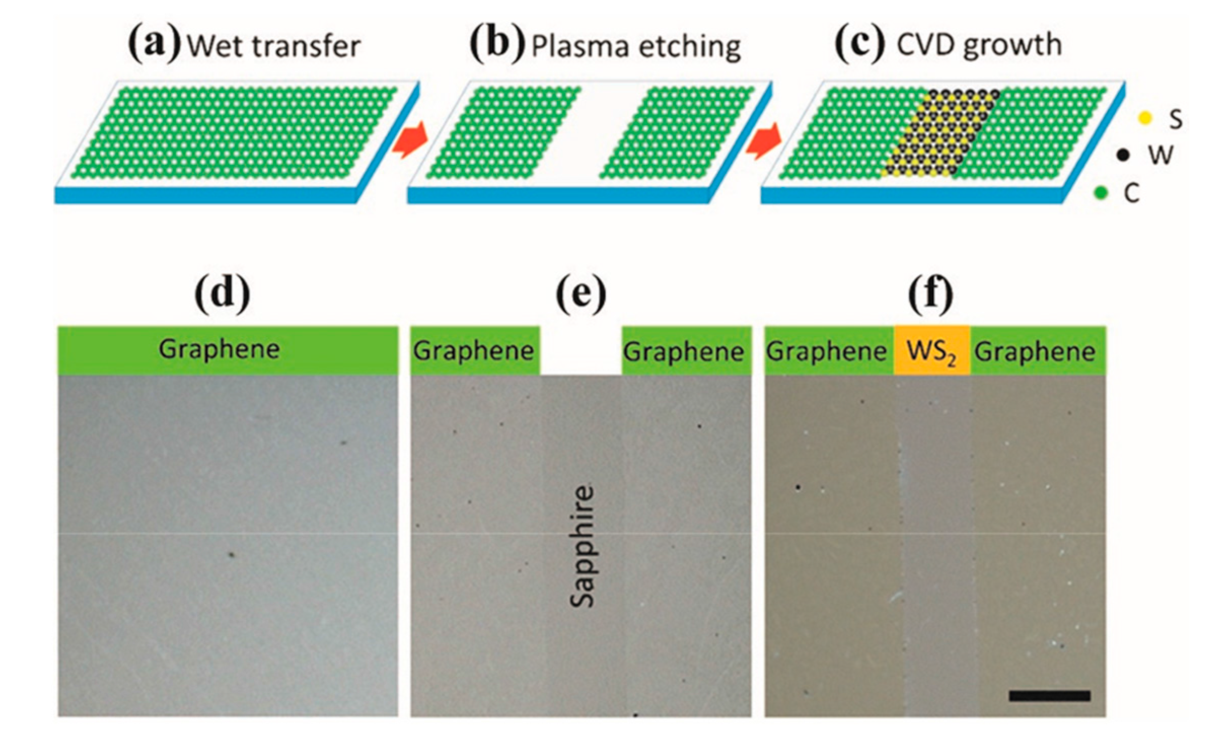
MoS2–graphene structure [82] were also fabricated by CVD method. Isolated hexagonal graphene grains were first synthesized by ambient-pressure CVD and then transferred onto a SiO2/Si substrate. After that, triangular single-layer MoS2 were grown on the graphene by reacting MoO3 and S in a pure Ar flow, which results in the formation of MoS2–graphene. The studies of electronics based on TMDs face challenges of making reliable electrical contacts to TMDs with low-ohmic contact resistance. Thus, Zheng et al. [83] came up with a seedless template-grown CVD method to prepare large-area graphene-WS2 heterojunctions and directly observed their 2D electrostatics and ohmic contacts. The preparation process is illustrated in Figure 8. Patterned graphene acted as the template for growing WS2 on sapphire. Monolayer WS2 selectively grew on the sapphire substrate and ultimately formed continuous films intimately connected to graphene (Figure 8c,f). This technique paves a new way to fabricate lateral graphene-TMDs heterostructures that can be transferred to various substrates.
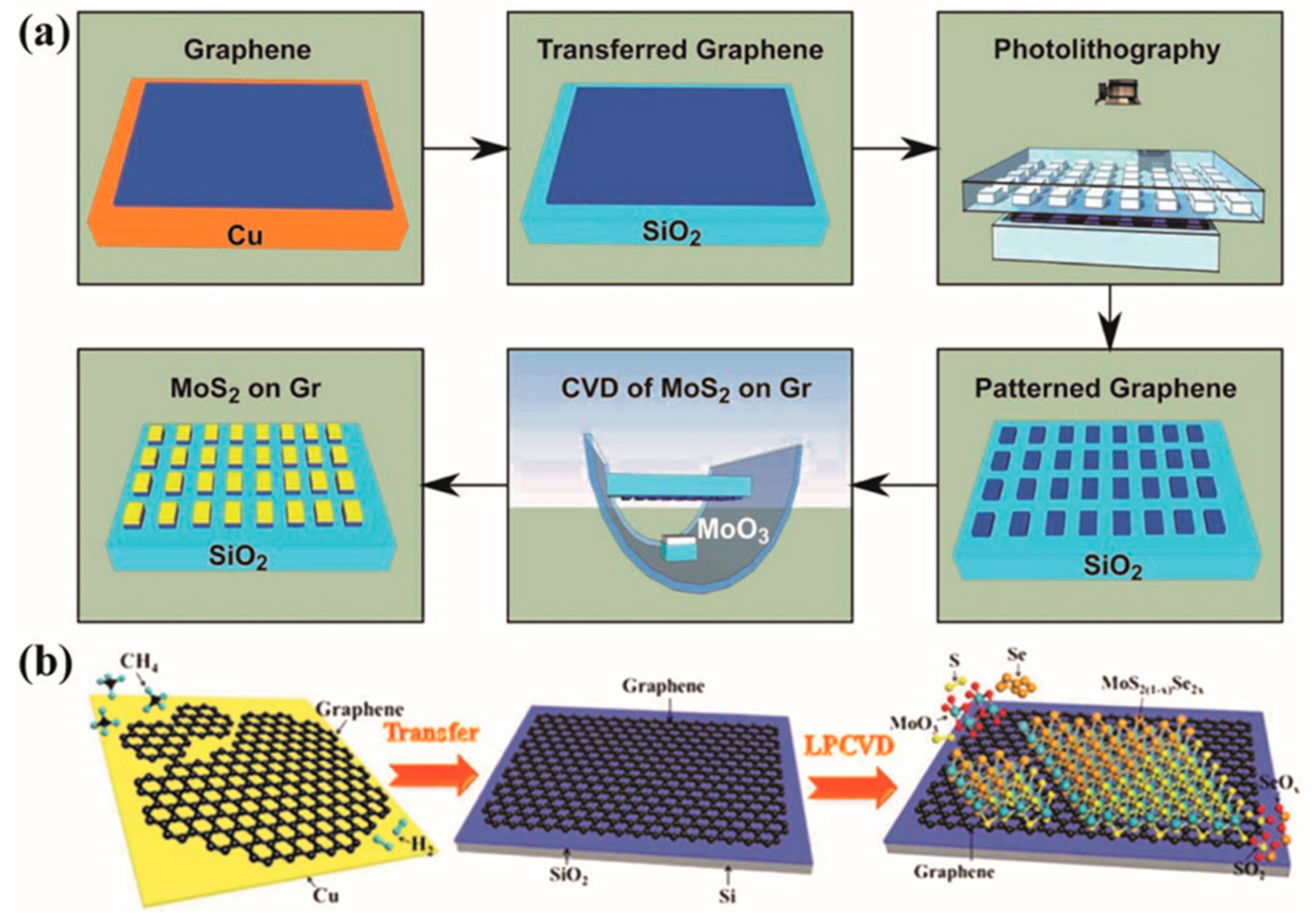
Lu et al. [84] reported a localized CVD growth of MoS2 on patterned graphene, and the specific processing steps are showed in Figure 9a. Graphene was grown on Cu foil and transferred into silica substrate firstly, and then the patterned graphene was obtained by using photolithography technique. In subsequent steps, the few-layer MoS2 has directly grown the top of the patterned graphene by CVD. Yue et al. [85] prepared the MoS2(1−x)Se2x–graphene heterostructure by growing a continuous high-quality monolayer MoS2(1−x)Se2x film on the transferred monolayer graphene film by using low-pressure CVD with different Se contents (Figure 9b). First, the monolayer graphene film was synthesized on a Cu foil and then transferred onto a SiO2/Si wafer. High-quality monolayer MoS2(1−x)Se2x films were grown on the graphene film using low-pressure CVD with different Se contents by adjusting the weight of the S and Se powders. Thus, the MoS2(1–x)Se2x–graphene heterostructures were obtained.
Yu et al. reported the preparation of precisely aligned MoS2 domains on the basal plane of h-BN by a low-pressure CVD method [86]. By using S and MoO3 powders as evaporation sources, high-quality monolayer MoS2 film was deposited on the h-BN substrates. MoS2–h-BN heterostructures with controlled MoS2 crystal morphology were also obtained by Antonelou’s group by using the same technique [87]. A heterostructure from a 1D-Bi2S3 nanowire and a 2D-MoS2 monolayer was achieved by the one-step CVD growth, in which a mixture of Bi2O3 and MoO3 nanopowder was chosen to be the precursor [88]. Besides, Gu et al. demonstrated, for the first time, the construction of high-quality TCI SnTe–Si heterostructures with excellent diode characteristics by a simple CVD process [89]. The fabrication was achieved by depositing polycrystalline SnTe films onto Si windows on pre-patterned SiO2/Si substrates. Wang et al. prepared n-type topological insulator Bi2Te3–p-Si junctions and characterized their photovoltaic responses [67].
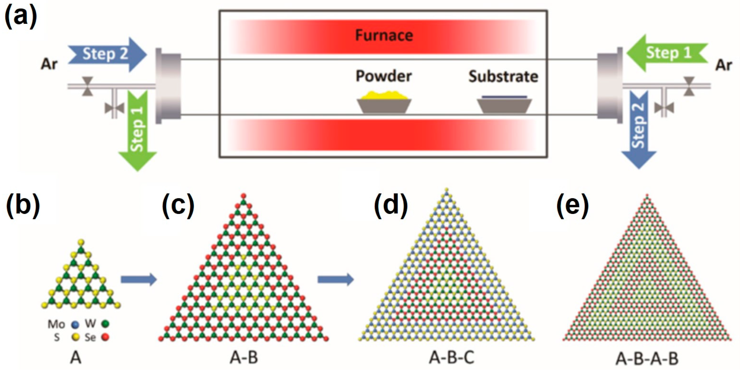
Very recently, Zhang et al. [90] reported a general synthetic strategy for highly robust growth of different kinds of heterostructures from two-dimensional (2D) crystals, such as diverse heterostructures, multi-heterostructures, and superlattices (Figure 10). Reverse flow is employed to grow heterostructures, which is crucial in the process. In the beginning, flow from the substrate to the source is applied during the temperature ramping and stabilization stage, which prevents impurities flow onto the substrate (step 1 in Figure 10a). After reaching the growth temperature, a reversed flow (from the source to the substrate) is applied to grow the heterostructures on the substrate (step 2 in Figure 10a). This procedure can be repeated several times to obtain multi-heterostructures (Figure 10c–e). Such robust synthesis of different heterostructures creates the system for fundamental studies and novel device demonstrations.
5. Molecular Beam Epitaxy (MBE) Method
Besides mechanical exfoliation, PVD/PVT, and CVD approach, the MBE technique has also been employed to grow diverse heterostructures that certainly including the TMDs-based kinds. MBE requires ultra-high vacuum (UHV). Elements with ultra-high purity are heated in an effusion cells or electron beam evaporators until they begin to slowly sublime. Then, the gaseous elements react with each other and condense on the substrate. The most important factor of MBE is the deposition rate and the slow deposition rate allows the films to grow epitaxially. The in situ reflection high-energy electron diffraction (RHEED) is always used for monitoring the growth of the crystal layers. It is an approach to grow crystalline and ultrathin heterostructures. By using this method, heterostructures coupling 2D TMDs and insulating h-BN were grown [96]. The van der Waals epitaxy growth approach provides the grown heterostructure film with undetectable misfit dislocations or strain despite large lattice mismatch.
6. Other Methods
There are multiple ways of fabricating heterostructures based on TMDs other than the methods aforementioned, including polymer-assisted transfer method, pulsed laser deposition (PLD), cation exchange, and wet chemical approach.
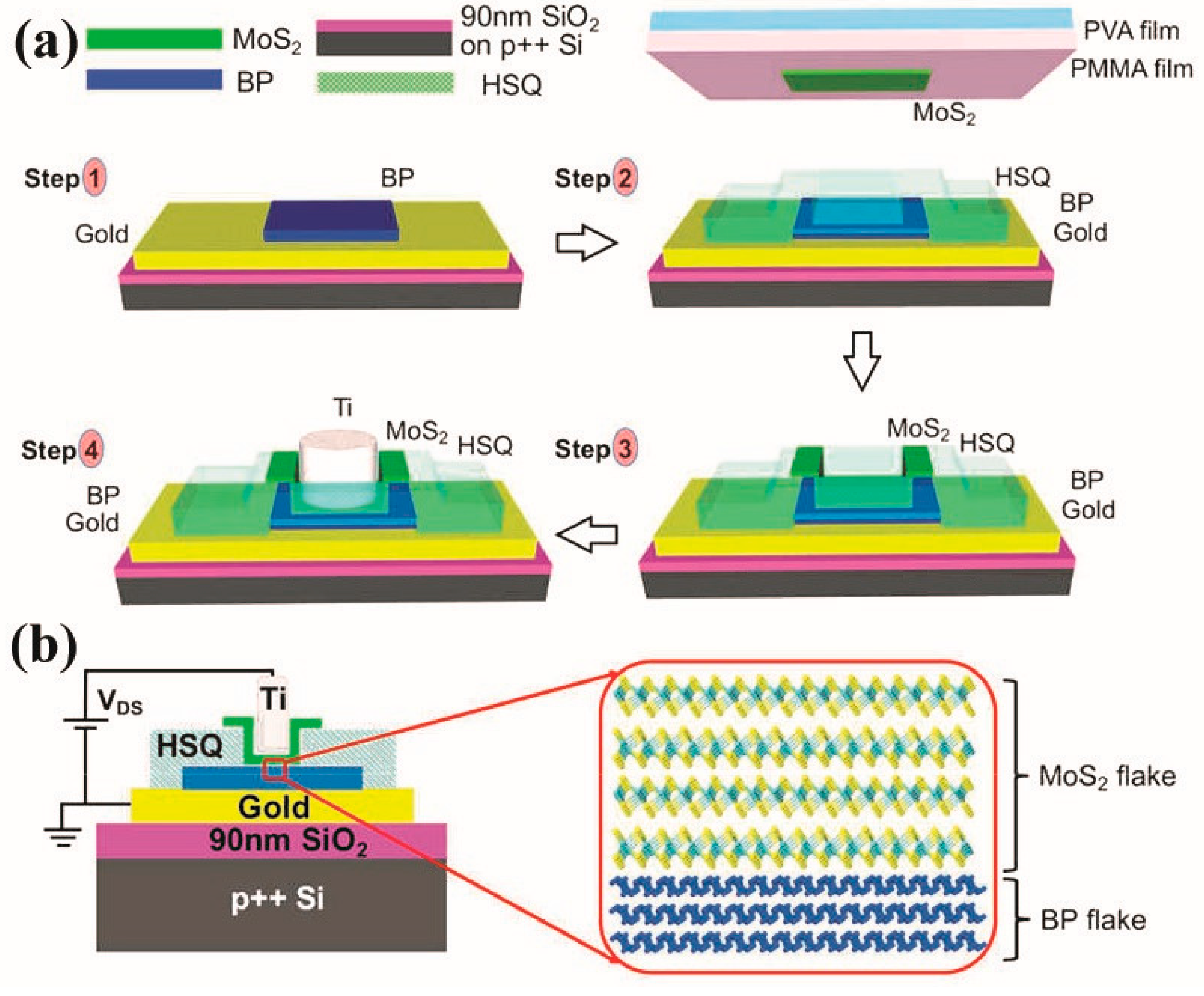
A polymer-assisted transfer method was employed using polyvinyl alcohol (PVA) and polymethylmethacrylate (PMMA) as a double stack film to form MoS2–BP vertical heterostructures (Figure 11) [69,97]. First, a mechanical exfoliated BP flake was placed onto the surface of a gold metal pad. Then, a layer of 70 nm hydrogen silsesquioxane (HSQ) is patterned on the BP flake but leaving an opening. After that, a MoS2 flake was transferred onto the BP flake where have the opening. After dissolving the PMMA film, a titanium electrode was deposited onto the top of the MoS2 flake. Such vertical heterostructures exhibit much smaller rectification in an atomically sharp p/n-junction.
The MoS2–WS2 heterostructure was prepared by transferring monolayer MoS2 onto monolayer WS2 on sapphire utilizing PMMA as the transfer “tool” [52]. Specifically, after the spin-coating of PMMA on CVD-grown MoS2 single layer, the PMMA/MoS2 film was separated from the substrate by KOH etching. In order to remove KOH residue under MoS2, the film was transferred to deionized water, followed by being transferred onto WS2 on sapphire and soaked in acetone to dissolve the PMMA. Tongay et al. fabricated the MoS2–WS2 heterostructures using PDMS as the transfer agent [98].
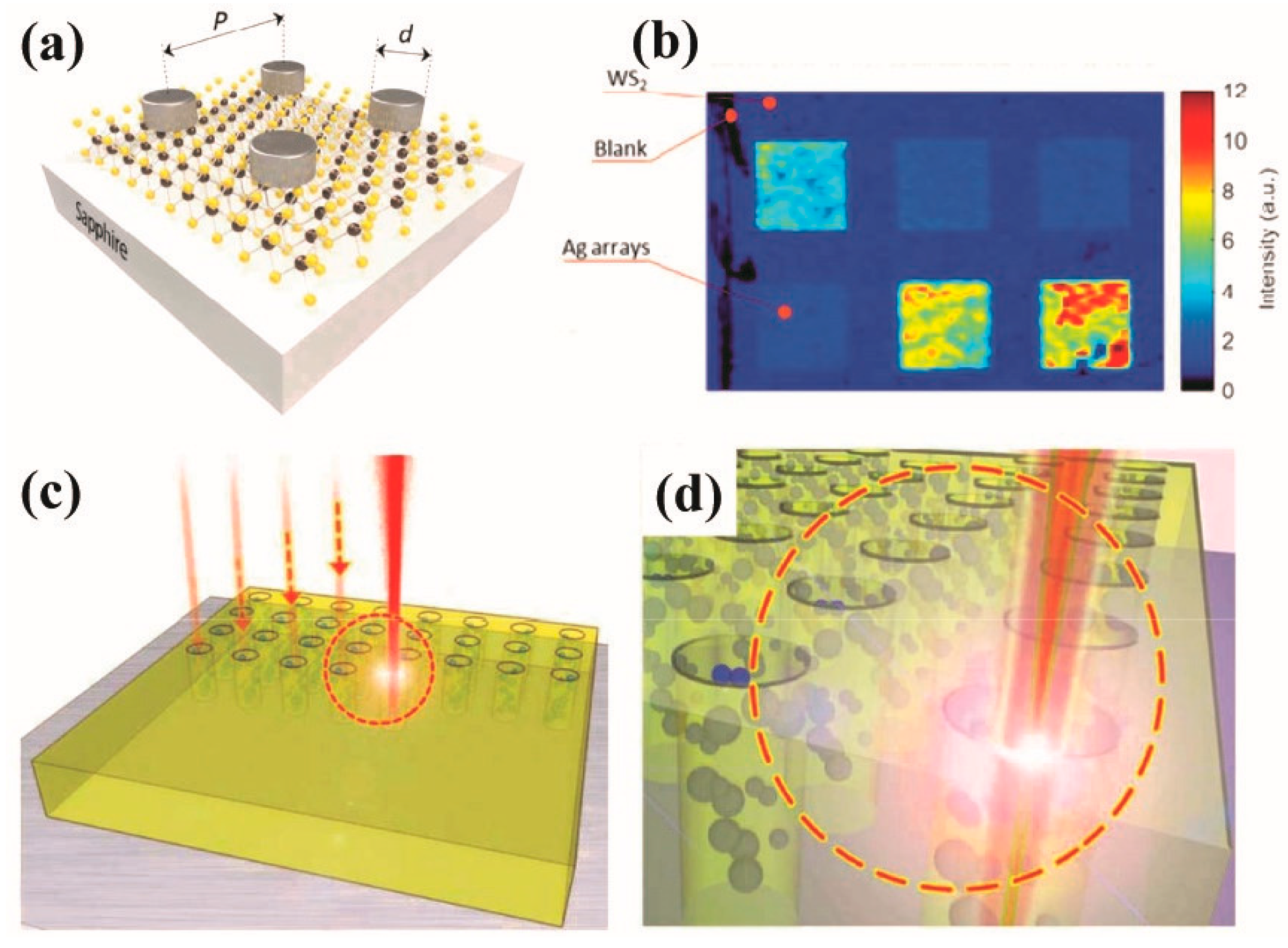
Butun et al. [99] utilized e-beam lithography techniques to fabricate Ag nanodisk arrays on WS2 monolayers to obtain Ag–WS2 heterostructure. WS2 monolayers were firstly prepared by typical CVD method. Then, Ag nanodisk arrays were deposited on WS2 monolayers by a standard e-beam lithography technique (Figure 12a). The Ag–WS2 heterostructure exhibit an enhanced PL due to the interaction between localized surface plasmon resonance of Ag nanodisks and WS2 (Figure 12b). Laser treatment technique can also be utilized to create heterojunctions. Ma et al. [100] prepared a WS2 thin film and porous WS2 structure was formed after laser treatment. Due to the high power of the laser, partially WS2 was oxidized to WO3. Thus the WS2–WO3 heterostructures were facile produced (Figure 12c,d).
Compared to other methods, PLD holds many merits in synthesizing high-quality heterostructures. PLD technique provides not only little contamination in products, but also obtains tunable thickness and large area samples. Moreover, the growth rate can be easily controlled by adjusting the experimental parameters. Yao et al. fabricated a WS2–Bi2Te3 heterostructure by successively depositing Bi2Te3 and WS2 films via PLD procedure [101].
Facile fabrication of MoS2 thin films on CdS nanowires was achieved by cation exchange in solution at room temperature [102]. Meanwhile, the magnetism in the MoS2–CdS heterostructure was studied. In detail, CdS nanowires can completely transform into MoS2 when being dipped into ethylene glycol containing 0.1 M MoCl4 for 6 h. An MoS2 shell with different thickness can be prepared by adjusting the reaction time.
Large-area films of vertical graphene–XS2 (X = W, Mo, or W and Mo alloy) heterostructures with dendritic-like morphology formed with alternating graphene and TMDs alloys are obtained by wet chemical routes. It was found that the resulting graphene–W0.4Mo0.6S2 films exhibit enhanced HER catalytic activity [103]. In this contribution, for the preparation of target alloy material, the mixture of (NH4)2WS4, (NH4)2MoS4 and graphene oxide solution was spin-coated on the Si/SiO2 substrate, and then went through the process of water evaporation and annealing.
We summarized the typical works for growing TMDs based 2D Heterostructures chronologically in Table 1.
7. Conclusions
The creation of van der Waals heterostructures has opened up a new paradigm for nanoscale materials and has enabled lots of extraordinary properties and devices. Great achievements in 2D materials have stimulated the exploration of 2D heterostructures over the past several years. These studies have brought us to a new world of heterostructures. In this review, we have summarized recent progress on the fabrication of heterostructures based on TMDs materials. Currently, most 2D heterostructures are synthesized by direct stacking of individual monolayer flakes of different materials. Although this method allows ultimate flexibility and many kinds of heterostructures can be easily prepared, it is slow and complicated. Especially, lateral heterostructures are difficult to prepare in this way. Thus, techniques of one-step growth of heterostructures are desired. In this case, direct growth of heterostructures by CVD, physical epitaxy, or the one-pot solution method are being developed. Especially, the CVD method has shown its advance in the direct growth of large-area and high-quality 2D heterostructures. More importantly, this route could lead to the formation of heterostructures consisting of lattice-aligned TMDs layers for both vertical and lateral cases. Knowing the route to obtain the heterostructures of 2D systems provides us the materials for investigating the interface phenomenon, device applications, etc. In addition, application-oriented growth of heterostructures could be an important field. For instance, toward catalyze application, we should take advantage of materials that have high catalytic activity with other materials that have high electrical conductivity. In order to have a better electronic transistor, designing a heterostructures that can solve the low on/off ratio of graphene and low carrier mobility of TMDCs will be a promising target. To realize this purpose, h-BN would be a good choice to be grown for the interface modification on the gate dielectric materials. Given the fast progress of 2D materials, we can expect that more and more techniques will be developed for obtained different kinds of heterostructures.
Acknowledgments
This work is supported by the start-up funding from Shaanxi Normal University, China (No. 1110010793), the National Natural Science Foundation of China (No. 51702203), the Fundamental Research Funds for the Central Universities (GK201603054), and the Young Talent Fund of the University Association for Science and Technology in Shaanxi, China (2017030014).
Author Contributions
Haimei Qi, Peng Hu, Fucai Liu, and Xuexia He designed the project and wrote the manuscript. Lina Wang, Jie Sun and Yi Long assisted manuscript writing. All authors commented on the manuscript.
Conflicts of Interest
The authors declare no conflict of interest.
References
- Novoselov, K.S.; Geim, A.K.; Morozov, S.V.; Jiang, D.; Zhang, Y.; Dubonos, S.V.; Grigorieva, I.V.; Firsov, A.A. Electric Field Effect in Atomically Thin Carbon Films. Science 2004, 306, 666–669. [Google Scholar] [CrossRef] [PubMed]
- Novoselov, K.S.; Jiang, D.; Schedin, F.; Booth, T.J.; Khotkevich, V.V.; Morozov, S.V.; Geim, A.K. Two-dimensional Atomic Crystals. Proc. Natl. Acad. Sci. USA 2005, 102, 10451–10453. [Google Scholar] [CrossRef] [PubMed]
- Wang, Q.H.; Kalantar-Zadeh, K.; Kis, A.; Coleman, J.N.; Strano, M.S. Electronics and optoelectronics of two-dimensional transition metal dichalcogenides. Nat. Nanotechnol. 2012, 7, 699–712. [Google Scholar] [CrossRef] [PubMed]
- Rivera, P.; Seyler, K.L.; Yu, H.; Schaibley, J.R.; Yan, J.; Mandrus, D.G.; Yao, W.; Xu, X. Valley-polarized Exciton Dynamics in a 2D Semiconductor Heterostructure. Science 2016, 351, 688–691. [Google Scholar] [CrossRef] [PubMed]
- Yu, W.J.; Li, Z.; Zhou, H.; Chen, Y.; Wang, Y.; Huang, Y.; Duan, X. Vertically Stacked Multi-heterostructures of Layered Materials for Logic Transistors and Complementary Inverters. Nat. Mater. 2013, 12, 246–252. [Google Scholar] [CrossRef] [PubMed]
- Yu, W.J.; Liu, Y.; Zhou, H.; Yin, A.; Li, Z.; Huang, Y.; Duan, X. Highly Efficient Gate-tunable Photocurrent Generation in Vertical Heterostructures of Layered Materials. Nat. Nanotechnol. 2013, 8, 952–958. [Google Scholar] [CrossRef] [PubMed]
- Hu, P.A.; Wen, Z.Z.; Wang, L.F.; Tan, P.H.; Xiao, K. Synthesis of Few-Layer GaSe Nanosheets for High Performance Photodetectors. ACS Nano 2012, 6, 5988–5994. [Google Scholar] [CrossRef] [PubMed]
- Wang, X.S.; Feng, H.B.; Wu, Y.M.; Jiao, L.Y. Controlled Synthesis of Highly Crystalline MoS2 Flakes by Chemical Vapor Deposition. J. Am. Chem. Soc. 2013, 135, 5304–5307. [Google Scholar] [CrossRef] [PubMed]
- Yang, Z.-X.; Han, N.; Fang, M.; Lin, H.; Cheung, H.-Y.; Yip, S.; Wang, E.-J.; Hung, T.; Wong, C.-Y.; Ho, J.C. Surfactant-assisted Chemical Vapour Deposition of High-performance Small-diameter GaSb Nanowires. Nat. Commun. 2014, 5, 5249. [Google Scholar] [CrossRef] [PubMed]
- Zhou, J.D.; Zeng, Q.S.; Lv, D.H.; Sun, L.F.; Niu, L.; Fu, W.; Liu, F.C.; Shen, Z.X.; Jin, C.H.; Liu, Z. Controlled Synthesis of High-Quality Mono layered alpha-In2Se3 via Physical Vapor Deposition. Nano Lett. 2015, 15, 6400–6405. [Google Scholar] [CrossRef] [PubMed]
- Gong, Y.J.; Lei, S.D.; Ye, G.L.; Li, B.; He, Y.M.; Keyshar, K.; Zhang, X.; Wang, Q.Z.; Lou, J.; Liu, Z.; et al. Two-Step Growth of Two-Dimensional WSe2/MoSe2 Heterostructures. Nano Lett. 2015, 15, 6135–6141. [Google Scholar] [CrossRef] [PubMed]
- Zhou, L.; Xu, K.; Zubair, A.; Liao, A.D.; Fang, W.J.; Ouyang, F.P.; Lee, Y.H.; Ueno, K.; Saito, R.; Palacios, T.; et al. Large-Area Synthesis of High-Quality Uniform Few-Layer MoTe2. J. Am. Chem. Soc. 2015, 137, 11892–11895. [Google Scholar] [CrossRef] [PubMed]
- Hu, P.; Ye, J.; He, X.; Du, K.; Zhang, K.K.; Wang, X.; Xiong, Q.; Liu, Z.; Jiang, H.; Kloc, C. Control of Radiative Exciton Recombination by Charge Transfer Induced Surface Dipoles in MoS2 and WS2 Monolayers. Sci. Rep. 2016, 6, 24105. [Google Scholar] [CrossRef] [PubMed]
- Tan, C.; Cao, X.; Wu, X.-J.; He, Q.; Yang, J.; Zhang, X.; Chen, J.; Zhao, W.; Han, S.; Nam, G.-H.; et al. Recent Advances in Ultrathin Two-Dimensional Nanomaterials. Chem. Rev. 2017, 117, 6225–6331. [Google Scholar] [CrossRef] [PubMed]
- Li, H.; Li, Y.; Aljarb, A.; Shi, Y.; Li, L.-J. Epitaxial Growth of Two-Dimensional Layered Transition-Metal Dichalcogenides: Growth Mechanism, Controllability, and Scalability. Chem. Rev. 2017. [Google Scholar] [CrossRef] [PubMed]
- Butler, S.Z.; Hollen, S.M.; Cao, L.; Cui, Y.; Gupta, J.A.; Gutiérrez, H.R.; Heinz, T.F.; Hong, S.S.; Huang, J.; Ismach, A.F.; et al. Progress, Challenges, and Opportunities in Two-Dimensional Materials Beyond Graphene. ACS Nano 2013, 7, 2898–2926. [Google Scholar] [CrossRef] [PubMed]
- Azizi, A.; Eichfeld, S.; Geschwind, G.; Zhang, K.; Jiang, B.; Mukherjee, D.; Hossain, L.; Piasecki, A.F.; Kabius, B.; Robinson, J.A.; et al. Freestanding van der Waals Heterostructures of Graphene and Transition Metal Dichalcogenides. ACS Nano 2015, 9, 4882–4890. [Google Scholar] [CrossRef] [PubMed]
- He, Y.; Yang, Y.; Zhang, Z.; Gong, Y.; Zhou, W.; Hu, Z.; Ye, G.; Zhang, X.; Bianco, E.; Lei, S.; et al. Strain-Induced Electronic Structure Changes in Stacked van der Waals Heterostructures. Nano Lett. 2016, 16, 3314–3320. [Google Scholar] [CrossRef] [PubMed]
- Aretouli, K.E.; Tsoutsou, D.; Tsipas, P.; Marquez-Velasco, J.; Aminalragia Giamini, S.; Kelaidis, N.; Psycharis, V.; Dimoulas, A. Epitaxial 2D SnSe2/2D WSe2 van der Waals Heterostructures. ACS Appl. Mater. Interfaces 2016, 8, 23222–23229. [Google Scholar] [CrossRef] [PubMed]
- Ray, K.; Yore, A.E.; Mou, T.; Jha, S.; Smithe, K.K.H.; Wang, B.; Pop, E.; Newaz, A.K.M. Photoresponse of Natural van der Waals Heterostructures. ACS Nano 2017, 11, 6024–6030. [Google Scholar] [CrossRef] [PubMed]
- Li, M.-Y.; Shi, Y.; Cheng, C.-C.; Lu, L.-S.; Lin, Y.-C.; Tang, H.-L.; Tsai, M.-L.; Chu, C.-W.; Wei, K.-H.; He, J.-H.; et al. Epitaxial Growth of a Monolayer WSe2-MoS2 Lateral p-n Junction with an Atomically Sharp Interface. Science 2015, 349, 524–528. [Google Scholar] [CrossRef] [PubMed]
- Gong, Y.; Lin, J.; Wang, X.; Shi, G.; Lei, S.; Lin, Z.; Zou, X.; Ye, G.; Vajtai, R.; Yakobson, B.I.; et al. Vertical and in-plane heterostructures from WS2/MoS2 monolayers. Nat. Mater. 2014, 13, 1135–1142. [Google Scholar] [CrossRef] [PubMed]
- Yoo, Y.; Degregorio, Z.P.; Johns, J.E. Seed Crystal Homogeneity Controls Lateral and Vertical Heteroepitaxy of Monolayer MoS2 and WS2. J. Am. Chem. Soc. 2015, 137, 14281–14287. [Google Scholar] [CrossRef] [PubMed]
- Tan, C.; Zhang, H. Epitaxial Growth of Hetero-Nanostructures Based on Ultrathin Two-Dimensional Nanosheets. J. Am. Chem. Soc. 2015, 137, 12162–12174. [Google Scholar] [CrossRef] [PubMed]
- Novoselov, K.S.; Mishchenko, A.; Carvalho, A.; Castro Neto, A.H. 2D Materials and Van der Waals Heterostructures. Science 2016, 353, aac9439. [Google Scholar] [CrossRef] [PubMed]
- Jariwala, D.; Marks, T.J.; Hersam, M.C. Mixed-dimensional van der Waals heterostructures. Nat. Mater. 2016, 16, 170–181. [Google Scholar] [CrossRef] [PubMed]
- Dean, C.R.; Young, A.F.; Meric, I.; Lee, C.; Wang, L.; Sorgenfrei, S.; Watanabe, K.; Taniguchi, T.; Kim, P.; Shepard, K.L.; et al. Boron Nitride Substrates for High-quality Graphene Electronics. Nat. Nanotechnol. 2010, 5, 722–726. [Google Scholar] [CrossRef] [PubMed]
- Xu, W.; Liu, W.; Schmidt, J.F.; Zhao, W.; Lu, X.; Raab, T.; Diederichs, C.; Gao, W.; Seletskiy, D.V.; Xiong, Q. Correlated fluorescence blinking in two-dimensional semiconductor heterostructures. Nature 2017, 541, 62–67. [Google Scholar] [CrossRef] [PubMed]
- Withers, F.; Del Pozo-Zamudio, O.; Mishchenko, A.; Rooney, A.P.; Gholinia, A.; Watanabe, K.; Taniguchi, T.; Haigh, S.J.; Geim, A.K.; Tartakovskii, A.I.; et al. Light-emitting Diodes by Band-structure Engineering in Van der Waals Heterostructures. Nat. Mater. 2015, 14, 301–306. [Google Scholar] [CrossRef] [PubMed]
- Withers, F.; Del Pozo-Zamudio, O.; Schwarz, S.; Dufferwiel, S.; Walker, P.M.; Godde, T.; Rooney, A.P.; Gholinia, A.; Woods, C.R.; Blake, P.; et al. WSe2 Light-Emitting Tunneling Transistors with Enhanced Brightness at Room Temperature. Nano Lett. 2015, 15, 8223–8228. [Google Scholar] [CrossRef] [PubMed]
- Mashhadi, S.; Duong, D.L.; Burghard, M.; Kern, K. Efficient Photothermoelectric Conversion in Lateral Topological Insulator Heterojunctions. Nano Lett. 2017, 17, 214–219. [Google Scholar] [CrossRef] [PubMed]
- Huo, N.; Kang, J.; Wei, Z.; Li, S.-S.; Li, J.; Wei, S.-H. Novel and Enhanced Optoelectronic Performances of Multilayer MoS2–WS2 Heterostructure Transistors. Adv. Funct. Mater. 2014, 24, 7025–7031. [Google Scholar] [CrossRef]
- Koppens, F.H.L.; Mueller, T.; Avouris, P.; Ferrari, A.C.; Vitiello, M.S.; Polini, M. Photodetectors Based on Graphene, other Two-dimensional Materials and Hybrid Systems. Nat. Nanotechnol. 2014, 9, 780–793. [Google Scholar] [CrossRef] [PubMed]
- Doan, M.-H.; Jin, Y.; Adhikari, S.; Lee, S.; Zhao, J.; Lim, S.C.; Lee, Y.H. Charge Transport in MoS2/WSe2 van der Waals Heterostructure with Tunable Inversion Layer. ACS Nano 2017, 11, 3832–3840. [Google Scholar] [CrossRef] [PubMed]
- Zhao, M.; Ye, Y.; Han, Y.; Xia, Y.; Zhu, H.; Wang, S.; Wang, Y.; Muller, D.A.; Zhang, X. Large-scale Chemical Assembly of Atomically Thin Transistors and Circuits. Nat. Nanotechnol. 2016, 11, 954–959. [Google Scholar] [CrossRef] [PubMed]
- Britnell, L.; Gorbachev, R.V.; Jalil, R.; Belle, B.D.; Schedin, F.; Mishchenko, A.; Georgiou, T.; Katsnelson, M.I.; Eaves, L.; Morozov, S.V.; et al. Field-Effect Tunneling Transistor Based on Vertical Graphene Heterostructures. Science 2012, 335, 947–950. [Google Scholar] [CrossRef] [PubMed] [Green Version]
- Roy, T.; Tosun, M.; Cao, X.; Fang, H.; Lien, D.-H.; Zhao, P.; Chen, Y.-Z.; Chueh, Y.-L.; Guo, J.; Javey, A. Dual-Gated MoS2/WSe2 van der Waals Tunnel Diodes and Transistors. ACS Nano 2015, 9, 2071–2079. [Google Scholar] [CrossRef] [PubMed]
- Sup Choi, M.; Lee, G.-H.; Yu, Y.-J.; Lee, D.-Y.; Hwan Lee, S.; Kim, P.; Hone, J.; Jong Yoo, W. Controlled Charge Trapping by Molybdenum Disulphide and Graphene in Ultrathin Heterostructured Memory Devices. Nat. Commun. 2013, 4, 1624. [Google Scholar] [CrossRef] [PubMed]
- Roy, K.; Padmanabhan, M.; Goswami, S.; Sai, T.P.; Ramalingam, G.; Raghavan, S.; Ghosh, A. Graphene-MoS2 Hybrid Structures for Multifunctional Photoresponsive Memory Devices. Nat. Nanotechnol. 2013, 8, 826–830. [Google Scholar] [CrossRef] [PubMed]
- Liu, Y.; Weiss, N.O.; Duan, X.; Cheng, H.-C.; Huang, Y.; Duan, X. Van der Waals heterostructures and devices. Nat. Rev. Mater. 2016, 1, 16042. [Google Scholar] [CrossRef]
- Frisenda, R.; Navarro-Moratalla, E.; Gant, P.; Perez De Lara, D.; Jarillo-Herrero, P.; Gorbachev, R.V.; Castellanos-Gomez, A. Recent progress in the assembly of nanodevices and van der Waals heterostructures by deterministic placement of 2D materials. Chem. Soc. Rev. 2018, 47, 53–68. [Google Scholar] [CrossRef] [PubMed]
- Geim, A.K.; Grigorieva, I.V. Van der Waals heterostructures. Nature 2013, 499, 419–425. [Google Scholar] [CrossRef] [PubMed]
- Lim, H.; Yoon, S.I.; Kim, G.; Jang, A.R.; Shin, H.S. Stacking of Two-Dimensional Materials in Lateral and Vertical Directions. Chem. Mater. 2014, 26, 4891–4903. [Google Scholar] [CrossRef]
- Bogaert, K.; Liu, S.; Chesin, J.; Titow, D.; Gradečak, S.; Garaj, S. Diffusion-Mediated Synthesis of MoS2/WS2 Lateral Heterostructures. Nano Lett. 2016, 16, 5129–5134. [Google Scholar] [CrossRef] [PubMed]
- Ullah, F.; Sim, Y.; Le, C.T.; Seong, M.-J.; Jang, J.I.; Rhim, S.H.; Tran Khac, B.C.; Chung, K.-H.; Park, K.; Lee, Y.; et al. Growth and Simultaneous Valley Manipulation of Two-Dimensional MoSe2-WSe2 Lateral Heterostructure. ACS Nano 2017, 11, 8822–8829. [Google Scholar] [CrossRef] [PubMed]
- Liu, Q.; Cook, B.; Gong, M.; Gong, Y.; Ewing, D.; Casper, M.; Stramel, A.; Wu, J. Printable Transfer-Free and Wafer-Size MoS2/Graphene van der Waals Heterostructures for High-Performance Photodetection. ACS Appl. Mater. Interfaces 2017, 9, 12728–12733. [Google Scholar] [CrossRef] [PubMed]
- Yang, W.; Chen, G.; Shi, Z.; Liu, C.-C.; Zhang, L.; Xie, G.; Cheng, M.; Wang, D.; Yang, R.; Shi, D.; et al. Epitaxial Growth of Single-domain Graphene on Hexagonal Boron Nitride. Nat. Mater. 2013, 12, 792–797. [Google Scholar] [CrossRef] [PubMed]
- Lotsch, B.V. Vertical 2D Heterostructures. Annu. Rev. Mater. Res. 2015, 45, 85–109. [Google Scholar] [CrossRef]
- Duan, X.D.; Wang, C.; Pan, A.L.; Yu, R.Q.; Duan, X.F. Two-dimensional Transition Metal Dichalcogenides as Atomically Thin Semiconductors: Opportunities and Challenges. Chem. Soc. Rev. 2015, 44, 8859–8876. [Google Scholar] [CrossRef] [PubMed]
- Wang, H.; Liu, F.C.; Fu, W.; Fang, Z.Y.; Zhou, W.; Liu, Z. Two-dimensional Heterostructures: Fabrication, Characterization, and Application. Nanoscale 2014, 6, 12250–12272. [Google Scholar] [CrossRef] [PubMed]
- Yi, M.; Shen, Z. A review on mechanical exfoliation for the scalable production of graphene. J. Mater. Chem. A 2015, 3, 11700–11715. [Google Scholar] [CrossRef]
- Hong, X.P.; Kim, J.; Shi, S.F.; Zhang, Y.; Jin, C.H.; Sun, Y.H.; Tongay, S.; Wu, J.Q.; Zhang, Y.F.; Wang, F. Ultrafast Charge Transfer in Atomically Thin MoS2/WS2 Heterostructures. Nat. Nanotechnol. 2014, 9, 682–686. [Google Scholar] [CrossRef] [PubMed]
- Rigos, A.F.; Hill, H.M.; Li, Y.L.; Chernikov, A.; Heinz, T.F. Probing Interlayer Interactions in Transition Metal Dichalcogenide Heterostructures by Optical Spectroscopy: MoS2/WS2 and MoSe2/WSe2. Nano Lett. 2015, 15, 5033–5038. [Google Scholar] [CrossRef] [PubMed]
- Nagler, P.; Plechinger, G.; Ballottin, M.V.; Mitioglu, A.; Meier, S.; Paradiso, N.; Strunk, C.; Chernikov, A.; Christianen, P.C.M.; Schüller, C.; et al. Interlayer Exciton Dynamics in a Dichalcogenide Monolayer Heterostructure. 2D Mater. 2017, 4, 025112. [Google Scholar] [CrossRef]
- Ceballos, F.; Bellus, M.Z.; Chiu, H.Y.; Zhao, H. Ultrafast Charge Separation and Indirect Exciton Formation in a MoS2-MoSe2 van der Waals Heterostructure. ACS Nano 2014, 8, 12717–12724. [Google Scholar] [CrossRef] [PubMed]
- Bellus, M.Z.; Ceballos, F.; Chiu, H.Y.; Zhao, H. Tightly Bound Trions in Transition Metal Dichalcogenide Heterostructures. ACS Nano 2015, 9, 6459–6464. [Google Scholar] [CrossRef] [PubMed]
- Roy, T.; Tosun, M.; Hettick, M.; Ahn, G.H.; Hu, C.; Javey, A. 2D-2D Tunneling Field-effect Transistors using WSe2/SnSe2 Heterostructures. Appl. Phys. Lett. 2016, 108, 083111. [Google Scholar] [CrossRef]
- Nourbakhsh, A.; Zubair, A.; Dresselhaus, M.S.; Palacios, T. Transport Properties of a MoS2/WSe2 Heterojunction Transistor and Its Potential for Application. Nano Lett. 2016, 16, 1359–1366. [Google Scholar] [CrossRef] [PubMed]
- Furchi, M.M.; Pospischil, A.; Libisch, F.; Burgdorfer, J.; Mueller, T. Photovoltaic Effect in an Electrically Tunable van der Waals Heterojunction. Nano Lett. 2014, 14, 4785–4791. [Google Scholar] [CrossRef] [PubMed]
- Shi, T.; Walker, R.C.; Jovanovic, I.; Robinson, J.A. Effects of Eenergetic Ion Irradiation on WSe2/SiC Heterostructures. Sci. Rep. 2017, 7, 4151. [Google Scholar] [CrossRef] [PubMed]
- Lopez-Sanchez, O.; Llado, E.A.; Koman, V.; Morral, A.F.I.; Radenovic, A.; Kis, A. Light Generation and Harvesting in a van der Waals Heterostructure. ACS Nano 2014, 8, 3042–3048. [Google Scholar] [CrossRef] [PubMed]
- Britnell, L.; Ribeiro, R.M.; Eckmann, A.; Jalil, R.; Belle, B.D.; Mishchenko, A.; Kim, Y.-J.; Gorbachev, R.V.; Georgiou, T.; Morozov, S.V.; et al. Strong Light-Matter Interactions in Heterostructures of Atomically Thin Films. Science 2013, 340, 1311–1314. [Google Scholar] [CrossRef] [PubMed]
- Li, D.W.; Xiong, W.; Jiang, L.J.; Xiao, Z.Y.; Golgir, H.R.; Wang, M.M.; Huang, X.; Zhou, Y.S.; Lin, Z.; Song, J.F.; et al. Multimodal Nonlinear Optical Imaging of MoS2 and MoS2-Based van der Waals Heterostructures. ACS Nano 2016, 10, 3766–3775. [Google Scholar] [CrossRef] [PubMed]
- Moriya, R.; Yamaguchi, T.; Inoue, Y.; Morikawa, S.; Sata, Y.; Masubuchi, S.; Machida, T. Large Current Modulation in Exfoliated-graphene/MoS2/metal Vertical Heterostructures. Appl. Phys. Lett. 2014, 105, 083119. [Google Scholar] [CrossRef]
- Chen, Z.S.; Biscaras, J.; Shukla, A. Optimal Light Harvesting in 2D Semiconductor Heterostructures. 2D Mater. 2017, 4, 025115. [Google Scholar] [CrossRef]
- Yan, X.; Liu, C.S.; Li, C.; Bao, W.Z.; Ding, S.J.; Zhang, D.W.; Zhou, P. Tunable SnSe2/WSe2 Heterostructure Tunneling Field Effect Transistor. Small 2017, 13, 1701478. [Google Scholar] [CrossRef] [PubMed]
- Ye, L.; Wang, P.; Luo, W.J.; Gong, F.; Liao, L.; Liu, T.D.; Tong, L.; Zang, J.F.; Xu, J.B.; Hu, W.D. Highly Polarization Sensitive Infrared Photodetector Based on Black Phosphorus-on-WSe2 Photogate Vertical Heterostructure. Nano Energy 2017, 37, 53–60. [Google Scholar] [CrossRef]
- Bettis Homan, S.; Sangwan, V.K.; Balla, I.; Bergeron, H.; Weiss, E.A.; Hersam, M.C. Ultrafast Exciton Dissociation and Long-Lived Charge Separation in a Photovoltaic Pentacene–MoS2 van der Waals Heterojunction. Nano Lett. 2017, 17, 164–169. [Google Scholar] [CrossRef] [PubMed]
- Zhou, R.P.; Ostwal, V.; Appenzeller, J. Vertical versus Lateral Two-Dimensional Heterostructures: On the Topic of Atomically Abrupt p/n-Junctions. Nano Lett. 2017, 17, 4787–4792. [Google Scholar] [CrossRef] [PubMed]
- Liu, F.; Chow, W.L.; He, X.; Hu, P.; Zheng, S.; Wang, X.; Zhou, J.; Fu, Q.; Fu, W.; Yu, P.; et al. Van der Waals p–n Junction Based on an Organic–Inorganic Heterostructure. Adv. Funct. Mater. 2015, 25, 5865–5871. [Google Scholar] [CrossRef]
- Zhang, H.B.; Man, B.Y.; Zhang, Q. Topological Crystalline Insulator SnTe/Si Vertical Heterostructure Photodetectors for High-Performance Near-Infrared Detection. ACS Appl. Mater. Interfaces 2017, 9, 14067–14077. [Google Scholar] [CrossRef] [PubMed]
- Westover, R.D.; Ditto, J.; Falmbigl, M.; Hay, Z.L.; Johnson, D.C. Synthesis and Characterization of Quaternary Monolayer Thick MoSe2/SnSe/NbSe2/SnSe Heterojunction Superlattices. Chem. Mater. 2015, 27, 6411–6417. [Google Scholar] [CrossRef]
- Ai, R.Q.; Guan, X.; Li, J.; Yao, K.K.; Chen, P.; Zhang, Z.W.; Duan, X.D.; Duan, X.F. Growth of Single-Crystalline Cadmium Iodide Nanoplates, CdI2/MoS2 (WS2, WSe2) Van der Waals Heterostructures, and Patterned Arrays. ACS Nano 2017, 11, 3413–3419. [Google Scholar] [CrossRef] [PubMed]
- Kim, Y.L.; Jung, J.H.; Yoon, H.S.; Song, M.S.; Bae, S.H.; Kim, Y.; Chen, Z.G.; Zou, J.; Joyce, H.J.; Gao, Q.; et al. CdS/CdSe Lateral Heterostructure Nanobelts by a Two-Step Physical Vapor Transport Method. Nanotechnology 2010, 21, 145602. [Google Scholar] [CrossRef] [PubMed]
- Behranginia, A.; Yasaei, P.; Majee, A.K.; Sangwan, V.K.; Long, F.; Foss, C.J.; Foroozan, T.; Fuladi, S.; Hantehzadeh, M.R.; Shahbazian-Yassar, R.; et al. Direct Growth of High Mobility and Low-Noise Lateral MoS2–Graphene Heterostructure Electronics. Small 2017, 13, 1604301. [Google Scholar] [CrossRef] [PubMed]
- Chen, X.S.; Qiu, Y.F.; Yang, H.H.; Liu, G.B.; Zheng, W.; Feng, W.; Cao, W.W.; Hu, W.P.; Hu, P.A. In-Plane Mosaic Potential Growth of Large-Area 2D Layered Semiconductors MoS2-MoSe2 Lateral Heterostructures and Photodetector Application. ACS Appl. Mater. Interfaces 2017, 9, 1684–1691. [Google Scholar] [CrossRef] [PubMed]
- Zhang, X.Q.; Lin, C.H.; Tseng, Y.W.; Huang, K.H.; Lee, Y.H. Synthesis of Lateral Heterostructures of Semiconducting Atomic Layers. Nano Lett. 2015, 15, 410–415. [Google Scholar] [CrossRef] [PubMed]
- Jung, Y.; Shen, J.; Sun, Y.; Cha, J.J. Chemically Synthesized Heterostructures of Two-Dimensional Molybdenum/Tungsten-Based Dichalcogenides with Vertically Aligned Layers. ACS Nano 2014, 8, 9550–9557. [Google Scholar] [CrossRef] [PubMed]
- Li, Y.; Cain, J.D.; Hanson, E.D.; Murthy, A.A.; Hao, S.Q.; Shi, F.Y.; Li, Q.Q.; Wolverton, C.; Chen, X.Q.; Dravid, V.P. Au@MoS2 Core-Shell Heterostructures with Strong Light-Matter Interactions. Nano Lett. 2016, 16, 7696–7702. [Google Scholar] [CrossRef] [PubMed]
- Lin, Y.C.; Bilgin, I.; Ahmed, T.; Chen, R.J.; Pete, D.; Kar, S.; Zhu, J.X.; Gupta, G.; Mohite, A.; Yoo, J. Charge Transfer in Crystalline Germanium/monolayer MoS2 Heterostructures Prepared by Chemical Vapor Deposition. Nanoscale 2016, 8, 18675–18681. [Google Scholar] [CrossRef] [PubMed]
- Turkdogan, S.; Fan, F.; Ning, C.Z. Color-Temperature Tuning and Control of Trichromatic White Light Emission from a Multisegment ZnCdSSe Heterostructure Nanosheet. Adv. Funct. Mater. 2016, 26, 8521–8526. [Google Scholar] [CrossRef]
- Ago, H.; Fukamachi, S.; Endo, H.; Solis-Fernandez, P.; Yunus, R.M.; Uchida, Y.; Panchal, V.; Kazakova, O.; Tsuji, M. Visualization of Grain Structure and Boundaries of Polycrystalline Graphene and Two-Dimensional Materials by Epitaxial Growth of Transition Metal Dichalcogenides. ACS Nano 2016, 10, 3233–3240. [Google Scholar] [CrossRef] [PubMed]
- Zheng, C.X.; Zhang, Q.H.; Weber, B.; Ilatikhameneh, H.; Chen, F.; Sahasrabudhe, H.; Rahman, R.; Li, S.Q.; Chen, Z.; Hellerstedt, J.; et al. Direct Observation of 2D Electrostatics and Ohmic Contacts in Template-Grown Graphene/WS2 Heterostructures. ACS Nano 2017, 11, 2785–2793. [Google Scholar] [CrossRef] [PubMed]
- Lu, F.; Karmakar, A.; Shahi, S.; Einarsson, E. Selective and Confined Growth of Transition Metal Dichalcogenides on Transferred Graphene. RSC Adv. 2017, 7, 37310–37314. [Google Scholar] [CrossRef]
- Yue, Y.C.; Feng, Y.Y.; Chen, J.C.; Zhang, D.H.; Feng, W. Two-Dimensional Large-scale Bandgap-tunable Monolayer MoS2(1−x)Se2x/graphene Heterostructures for Phototransistors. J. Mater. Chem. C 2017, 5, 5887–5896. [Google Scholar] [CrossRef]
- Yu, H.; Yang, Z.Z.; Du, L.J.; Zhang, J.; Shi, J.N.; Chen, W.; Chen, P.; Liao, M.Z.; Zhao, J.; Meng, J.L.; et al. Precisely Aligned Monolayer MoS2 Epitaxially Grown on h-BN basal Plane. Small 2017, 13, 1603005. [Google Scholar] [CrossRef] [PubMed]
- Antonelou, A.; Hoffman, T.; Edgar, J.H.; Yannopoulos, S.N. MoS2/h-BN Heterostructures: Controlling MoS2 Crystal Morphology by Chemical Vapor Deposition. J. Mater. Sci. 2017, 52, 7028–7038. [Google Scholar] [CrossRef]
- Li, Y.T.; Huang, L.; Li, B.; Wang, X.T.; Zhou, Z.Q.; Li, J.B.; Wei, Z.M. Co-nucleus 1D/2D Heterostructures with Bi2S3 Nanowire and MoS2 Monolayer: One-Step Growth and Defect-Induced Formation Mechanism. ACS Nano 2016, 10, 8938–8946. [Google Scholar] [CrossRef] [PubMed]
- Gu, S.H.; Ding, K.; Pan, J.; Shao, Z.B.; Mao, J.; Zhang, X.J.; Jie, J.S. Self-driven, Broadband and Ultrafast Photovoltaic Detectors Based on Topological Crystalline Insulator SnTe/Si Heterostructures. J. Mater. Chem. A 2017, 5, 11171–11178. [Google Scholar] [CrossRef]
- Zhang, Z.; Chen, P.; Duan, X.; Zang, K.; Luo, J.; Duan, X. Robust Epitaxial Growth of Two-dimensional Heterostructures, Multiheterostructures, and Superlattices. Science 2017, 357, 788–792. [Google Scholar] [CrossRef] [PubMed]
- Nikam, R.D.; Sonawane, P.A.; Sankar, R.; Chen, Y.T. Epitaxial Growth of Vertically Stacked p-MoS2/n-MoS2 Heterostructures by Chemical Vapor Deposition for Light Emitting Devices. Nano Energy 2017, 32, 454–462. [Google Scholar] [CrossRef]
- Samad, L.; Bladow, S.M.; Ding, Q.; Zhuo, J.Q.; Jacobberger, R.M.; Arnold, M.S.; Jin, S. Layer-Controlled Chemical Vapor Deposition Growth of MoS2 Vertical Heterostructures via van der Waals Epitaxy. ACS Nano 2016, 10, 7039–7046. [Google Scholar] [CrossRef] [PubMed]
- Zhang, X.W.; Meng, F.; Christianson, J.R.; Arroyo-Torres, C.; Lukowski, M.A.; Liang, D.; Schmidt, J.R.; Jin, S. Vertical Heterostructures of Layered Metal Chalcogenides by van der Waals Epitaxy. Nano Lett. 2014, 14, 3047–3054. [Google Scholar] [CrossRef] [PubMed]
- Duan, X.D.; Wang, C.; Shaw, J.C.; Cheng, R.; Chen, Y.; Li, H.L.; Wu, X.P.; Tang, Y.; Zhang, Q.L.; Pan, A.L.; et al. Lateral Epitaxial Growth of Two-Dimensional Layered Semiconductor Heterojunctions. Nat. Nanotechnol. 2014, 9, 1024–1030. [Google Scholar] [CrossRef] [PubMed]
- Li, S.; Wang, S.; Tang, D.-M.; Zhao, W.; Xu, H.; Chu, L.; Bando, Y.; Golberg, D.; Eda, G. Halide-assisted Atmospheric Pressure Growth of Large WSe2 and WS2 Monolayer Crystals. Appl. Mater. Today 2015, 1, 60–66. [Google Scholar] [CrossRef]
- Barton, A.T.; Yue, R.; Anwar, S.; Zhu, H.; Peng, X.; McDonnell, S.; Lu, N.; Addou, R.; Colombo, L.; Kim, M.J.; et al. Transition Metal Dichalcogenide and Hexagonal Boron Nitride Heterostructures Grown by Molecular Beam Epitaxy. Microelectron. Eng. 2015, 147, 306–309. [Google Scholar] [CrossRef]
- Castellanos-Gomez, A.; Buscema, M.; Molenaar, R.; Singh, V.; Janssen, L.; van der Zant, H.S.; Steele, G.A. Deterministic transfer of two-dimensional materials by all-dry viscoelastic stamping. 2D Mater. 2014, 1, 011002. [Google Scholar]
- Tongay, S.; Fan, W.; Kang, J.; Park, J.; Koldemir, U.; Suh, J.; Narang, D.S.; Liu, K.; Ji, J.; Li, J.B.; et al. Tuning Interlayer Coupling in Large-Area Heterostructures with CVD-Grown MoS2 and WS2 Monolayers. Nano Lett. 2014, 14, 3185–3190. [Google Scholar] [CrossRef] [PubMed]
- Butun, S.; Palacios, E.; Cain, J.D.; Liu, Z.Z.; Dravid, V.P.; Aydin, K. Quantifying Plasmon-Enhanced Light Absorption in Monolayer WS2 Films. ACS Appl. Mater. Interfaces 2017, 9, 15044–15051. [Google Scholar] [CrossRef] [PubMed]
- Ma, S.N.; Zeng, L.L.; Tao, L.L.; Tang, C.Y.; Yuan, H.Y.; Long, H.; Cheng, P.K.; Chai, Y.; Chen, C.S.; Fung, K.H.; et al. Enhanced Photocatalytic Activity of WS2 Film by Laser Drilling to Produce Porous WS2/WO3 Heterostructure. Sci. Rep. 2017, 7, 3125. [Google Scholar] [CrossRef] [PubMed]
- Yao, J.D.; Zheng, Z.Q.; Yang, G.W. Layered-material WS2/topological insulator Bi2Te3 Heterostructure Photodetector with Ultrahigh Responsivity in the Range from 370 to 1550 nm. J. Mater. Chem. C 2016, 4, 7831–7840. [Google Scholar] [CrossRef]
- Tan, C.S.; Lu, Y.J.; Chen, C.C.; Liu, P.H.; Gwo, S.; Guo, G.Y.; Chen, L.J. Magnetic MoS2 Interface Monolayer on a CdS Nanowire by Cation Exchange. J. Phys. Chem. C 2016, 120, 23055–23060. [Google Scholar] [CrossRef]
- Lei, Y.; Pakhira, S.; Fujisawa, K.; Wang, X.Y.; Iyiola, O.O.; Lopez, N.P.; Elias, A.L.; Rajukumar, L.P.; Zhou, C.J.; Kabius, B.; et al. Low-temperature Synthesis of Heterostructures of Transition Metal Dichalcogenide Alloys (WxMo1−xS2) and Graphene with Superior Catalytic Performance for Hydrogen Evolution. ACS Nano 2017, 11, 5103–5112. [Google Scholar] [CrossRef] [PubMed]
Figure 1.
Schematic illustration of the preparation of lateral heterostructure and vertical heterostructure (transition metal dichalcogenides (TMDs) are examples in Figure 1): (a) First TMD layer on substrate. (b) Second TMD layer construct with the first TMD layer. (c) Two types TMDs construct to lateral heterostructure. (d) Two types TMDs construct to vertical heterostructure.

Figure 2.
An illustrative procedure of the Scotch tape–based micromechanical cleavage of graphene. Data are reproduced with permission from [51]. Copyright © 2015, Royal Society of Chemistry.
Figure 2.
An illustrative procedure of the Scotch tape–based micromechanical cleavage of graphene. Data are reproduced with permission from [51]. Copyright © 2015, Royal Society of Chemistry.

Figure 3.
Mechanical exfoliation methods: (a) Optical image of a MoS2 flake that contains a monolayer (ML) region. (b) Optical image of a MoSe2 ML. (c) the MoS2–MoSe2 heterostructure. (d) Optical image of MoS2–graphene heterostructure. (e) Atomic force microscopy (AFM) morphology of MoS2-graphene heterostructures. (a–c) are reproduced with permission from [55]. Copyright © 2014, American Chemical Society. (d,e) are reproduced with permission from [63]. Copyright © 2016, American Chemical Society.

Figure 4.
(a) Optical image of the device based on a vertical BP–WSe2 heterostructure. (b,c) AFM height images of the surface morphology of the junction. The size bar is 15 µm. (d) Schematic of the WSe2–SnSe2 van der Waals heterostructure (not to scale) with a flake of SnSe2 transferred to a flake of WSe2 on a silicon substrate with Al2O3 as a dielectric. The inset shows the crystal structure of SnSe2 and WSe2. (e) Atomic force microscope image of the device based on WSe2–SnSe2 van der Waals heterostructure. (f) Cross-sectional TEM image of WSe2–SnSe2 van der Waals heterostructure. Scale bar, 5 nm. (a,b) are reproduced with permission from [67]. Copyright © 2017 Elsevier Ltd. (c–e) are reproduced with permission from [66]. Copyright © 2017 John Wiley & Sons, Inc.

Figure 5.
(a–c) Side view, (d–f) top view and (g–i) typical optical images of the fabrication process of the organic-inorganic heterostructures fabrication process. Data are reproduced with permission from [70]. Copyright © 2015 John Wiley & Sons, Inc.
Figure 5.
(a–c) Side view, (d–f) top view and (g–i) typical optical images of the fabrication process of the organic-inorganic heterostructures fabrication process. Data are reproduced with permission from [70]. Copyright © 2015 John Wiley & Sons, Inc.

Figure 6.
(a) Schematic of the physical vapor deposition apparatus. (b) Optical image of a CdI2–WSe2, CdI2–WS2 and CdI2–MoS2 heterostructure. (a) is reproduced with permission from [71]. Copyright © 2017, American Chemical Society. (b) are reproduced with permission from [73]. Copyright © 2017, American Chemical Society.

Figure 7.
Chemical vapor deposition (CVD) method: (a) Schematic illustration of the two-step CVD technique for the preparation of mosaic MoS2–MoSe2 lateral heterojunctions film on SiO2/Si substrate. (b) Schematic illustration of the synthesis setup and various modes of hetero-epitaxial growth of TMD atomic layers. (c) Schematic showing the CVD process of MoS2 shell growth on Au nanoparticles. (a) is reproduced with permission from [76]. Copyright © 2017, American Chemical Society. (b) is reproduced with permission from [77]. Copyright © 2015, American Chemical Society. (c) is reproduced with permission from [79]. Copyright © 2016, American Chemical Society.

Figure 8.
Schematic illustration of the steps of preparing a graphene–WS2 heterojunction: (a) wet transfer of CVD graphene on a sapphire substrate, (b) patterning the graphene by lithography and O2 plasma etching, and (c) selective growth of WS2 monolayer connecting to graphene. (d–f) Optical images are corresponding to the three steps. The scale bar is 20 μm and can be applied to all the images. Data are reproduced with permission from [83]. Copyright © 2017, American Chemical Society.

Figure 9.
(a) Illustration of processing steps (clockwise from top left) resulting in localized CVD growth of MoS2 on patterned graphene. (b) Schematic illustration of the growth of the MoS2(1−x)Se2x–graphene heterostructure. (a) is reproduced with permission from [84]. Copyright © 2017, Royal Society of Chemistry. (b) is reproduced with permission from [85]. Copyright © 2017, Royal Society of Chemistry.

Figure 10.
The robust epitaxial growth of 2D monolayer heterostructures, multiheterostructures, and superlattices with a modified CVD process. (a) Schematic illustration of a modified CVD system for the robust epitaxial growth of lateral heterostructures. (b) monolayer seed A. (c) A-B heterostructure. (d) A-B-C multiheterostructures. (e) A-B-A-B superlattices. Data are reproduced with permission from [90]. Copyright © 2017, American Association for the Advancement of Science.

Figure 11.
(a) Graphic representation of the fabrication process flow for the vertical devices: Step 1, BP flake is peeled onto a gold pad, which is deposited on a 90 nm SiO2/p++ Si substrate. Step 2, an HSQ mask is created by e-beam lithography, serving as an isolation layer, leaving an opening to the BP flake. Step 3, MoS2 is transferred and the supporting film is dissolved. Step 4, the top electrode is deposited in the opening region and across the isolation layer. (b) Cross section view of a vertical device. A Ti electrode serves as the drain and the gold pad serves as the source in this 2-terminal device. Data are reproduced with permission from [69]. Copyright © 2017, American Chemical Society.

Figure 12.
(a) A conceptual schematic of the proposed WS2–Ag plasmonic heterostructure on sapphire. (b) 2D photoluminescence measurement of the fabricated plasmonic Ag arrays with periodicity 300 nm. (c) Schematic diagram of nanosecond pulse laser treatment on samples with a moving laser beam. (d) Zoom-in structural model of porous WS2 film after laser treatment. (a,b) are reproduced with permission from [99]. Copyright © 2017, American Chemical Society. (c,d) are reproduced with permission from [100]. Copyright © 2017, Rights Managed by Nature Publishing Group.


Table 1.
Typical works of TMDs based 2D heterostructures.
| Heterostructures | Method | Type | Year | Reference |
|---|---|---|---|---|
| WS2/MoS2 | CVD | Vertical and Lateral | 2014 | [22] |
| WS2/MoS2 | Mechanical exfoliation | Vertical | 2014 | [32] |
| WS2/MoS2 | CVD | Vertical and Lateral | 2015 | [23] |
| WSe2–MoS2 | CVD | Lateral | 2015 | [21] |
| WSe2/MoSe2 | CVD | Vertical and Lateral | 2015 | [11] |
| Rubrene/MoS2` | Mechanical exfoliation | Vertical | 2015 | [70] |
| MoSe2/SnSe/NbSe2/SnSe | Mechanical and chemical exfoliation | Vertical | 2015 | [72] |
| SnSe2/WSe2 | Molecular beam epitaxy | Vertical | 2016 | [19] |
| Ge/MoS2 | CVD | Vertical | 2016 | [80] |
| SnSe2/WSe2 | Mechanical exfoliation | Vertical | 2016 | [57] |
| MoS2/WS2 | CVD | Lateral | 2016 | [44] |
| MoSe2/WSe2 | Pulsed-laser-deposition-assisted selenization | Lateral | 2017 | [45] |
| WSe2/SiC | Mechanical exfoliation | Vertical | 2017 | [60] |
| BP/WSe2 | Mechanical exfoliation | Vertical | 2017 | [67] |
| SnSe2/WSe2 | Mechanical exfoliation | Vertical | 2017 | [66] |
| Pentacene–MoS2 | PVT | Vertical | 2017 | [68] |
| CdI2/MoS2 (WS2, WSe2) | PVT | Vertical | 2017 | [73] |
| MoS2/Graphene | CVD | Lateral | 2017 | [75] |
| WS2/Graphene | CVD | Vertical | 2017 | [83] |
| h-BN/MoS2 | CVD | Vertical | 2017 | [87] |
| WS2/WO3 | Laser drilling | Vertical | 2017 | [100] |
© 2018 by the authors. Licensee MDPI, Basel, Switzerland. This article is an open access article distributed under the terms and conditions of the Creative Commons Attribution (CC BY) license (http://creativecommons.org/licenses/by/4.0/).
Share and Cite
MDPI and ACS Style
Qi, H.; Wang, L.; Sun, J.; Long, Y.; Hu, P.; Liu, F.; He, X. Production Methods of Van der Waals Heterostructures Based on Transition Metal Dichalcogenides. Crystals 2018, 8, 35. https://doi.org/10.3390/cryst8010035
AMA Style
Qi H, Wang L, Sun J, Long Y, Hu P, Liu F, He X. Production Methods of Van der Waals Heterostructures Based on Transition Metal Dichalcogenides. Crystals. 2018; 8(1):35. https://doi.org/10.3390/cryst8010035
Chicago/Turabian StyleQi, Haimei, Lina Wang, Jie Sun, Yi Long, Peng Hu, Fucai Liu, and Xuexia He. 2018. "Production Methods of Van der Waals Heterostructures Based on Transition Metal Dichalcogenides" Crystals 8, no. 1: 35. https://doi.org/10.3390/cryst8010035
Note that from the first issue of 2016, this journal uses article numbers instead of page numbers. See further details here.