Properties of Nitrogen/Silicon Doped Vertically Oriented Graphene Produced by ICP CVD Roll-to-Roll Technology

 ,
,
Abstract
:1. Introduction
2. Materials and Methods
2.1. Materials
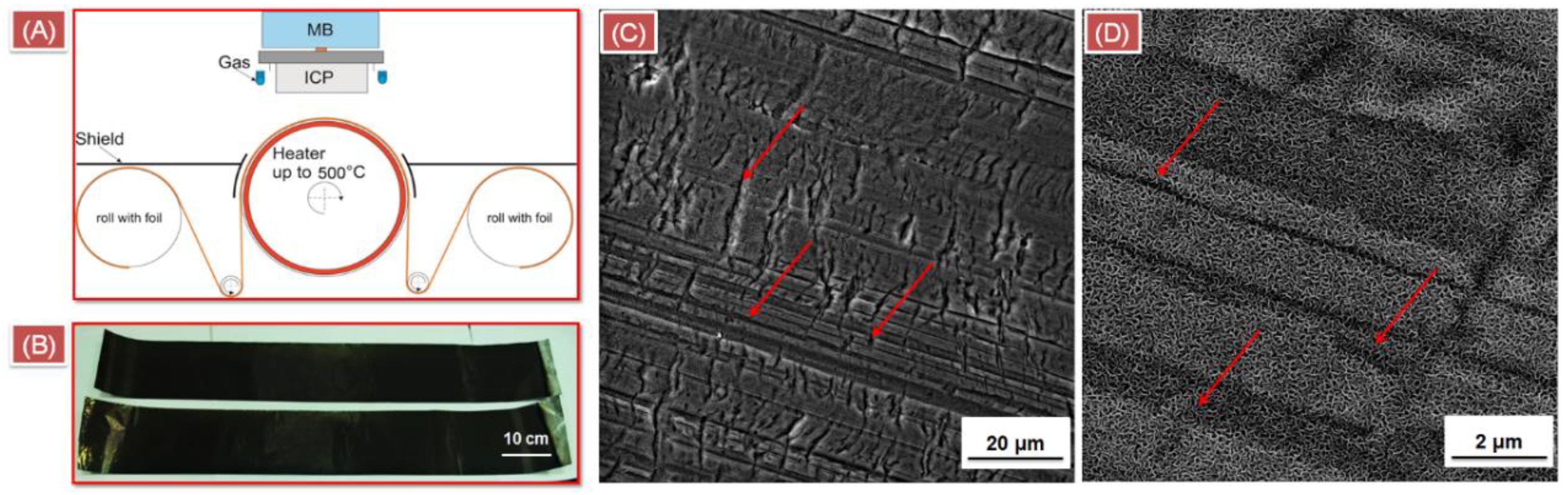
2.2. Methods
2.3. Characterization
3. Results and Discussion
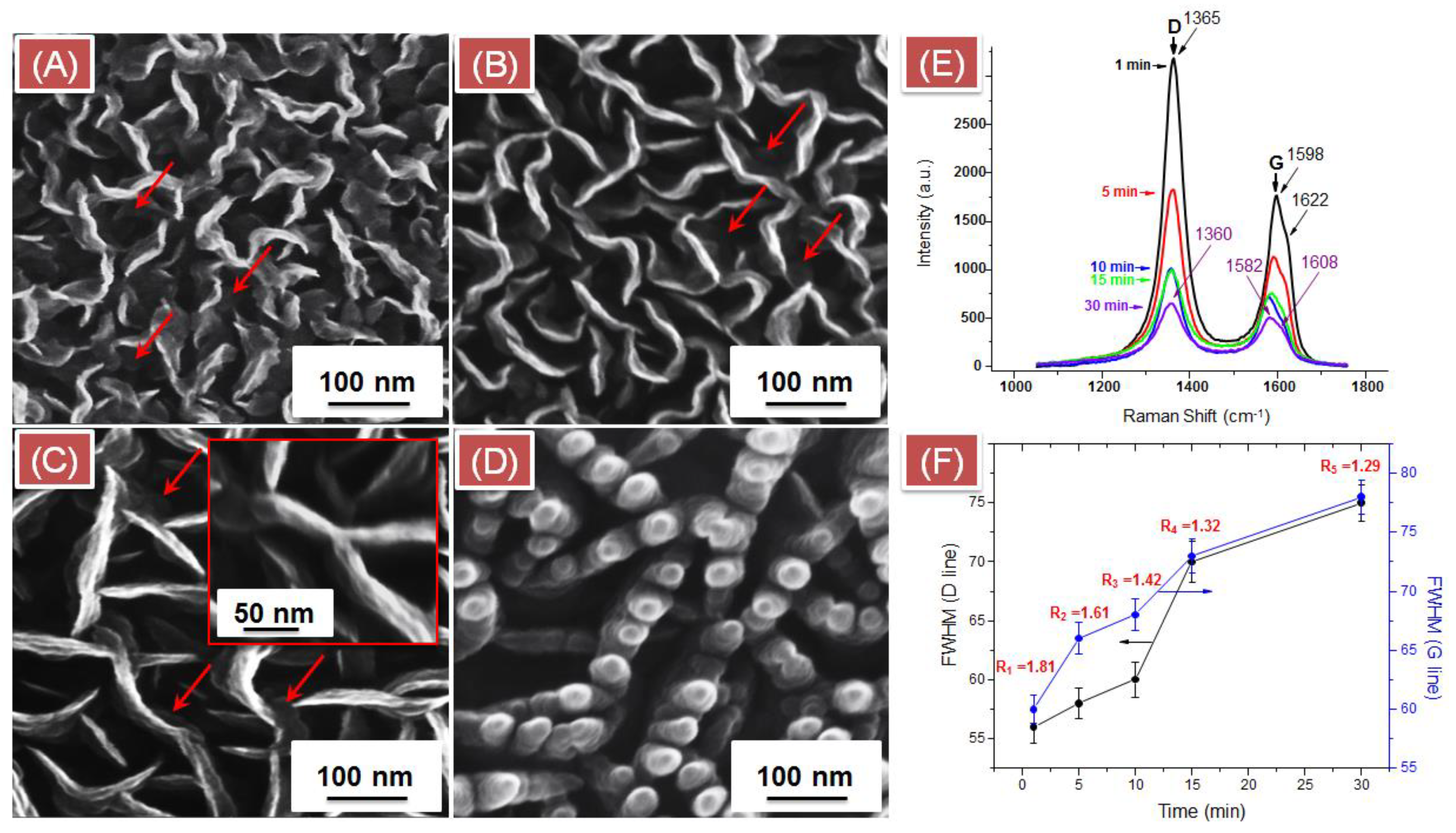
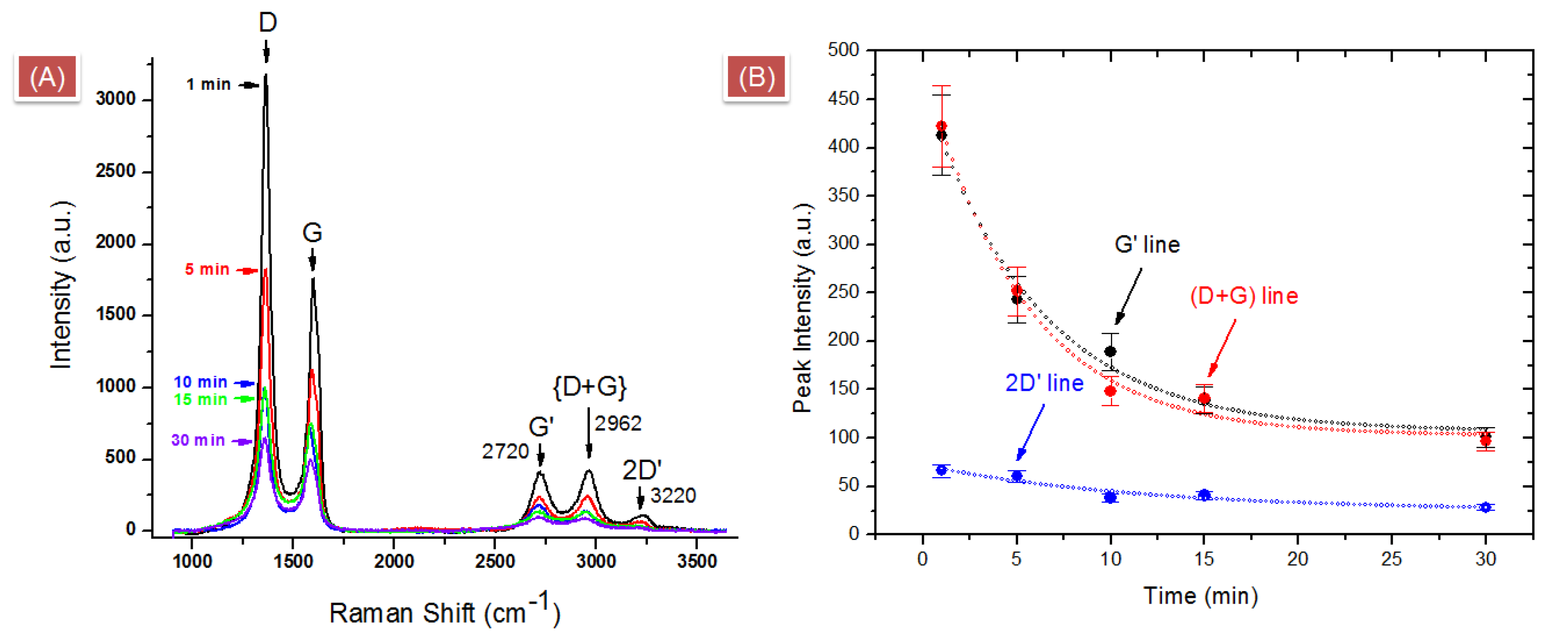
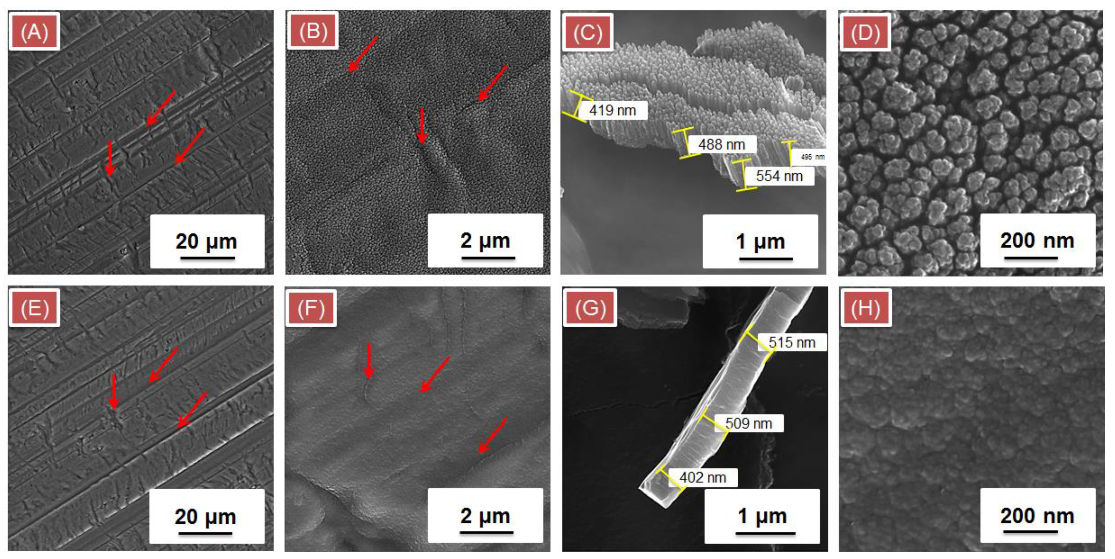
3.1. Effect of Deposition Time at Isothermal (450 °C) and Isobaric (1.0 Pa) Conditions
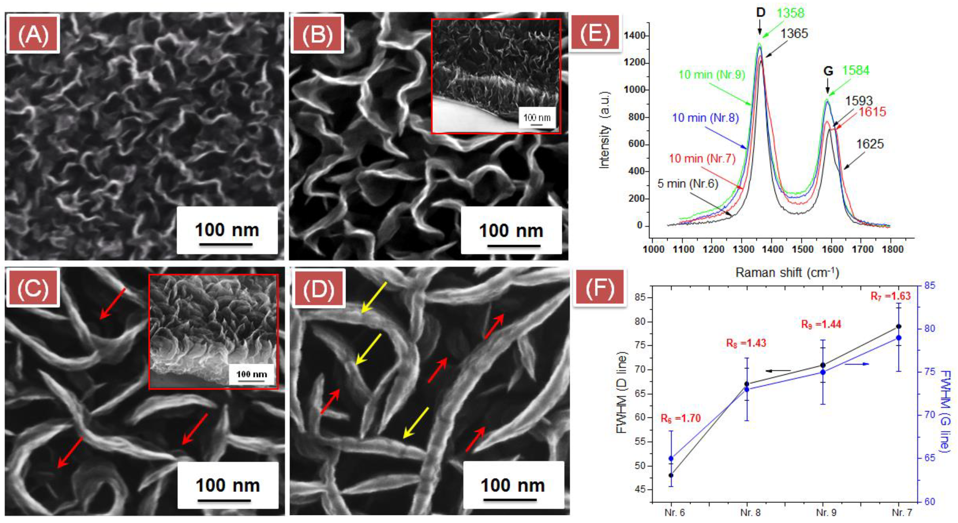
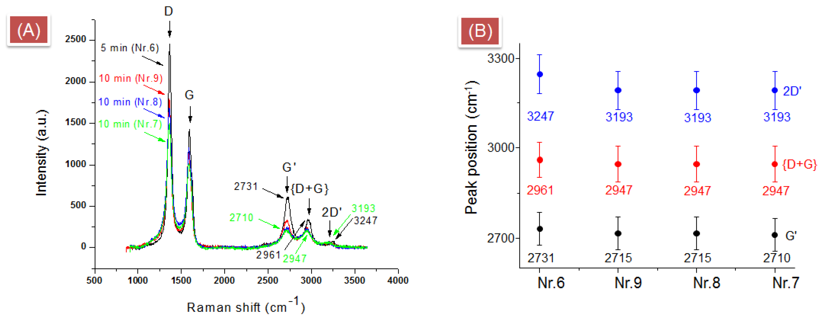
3.2. Effect of Partial Pressure of Propane
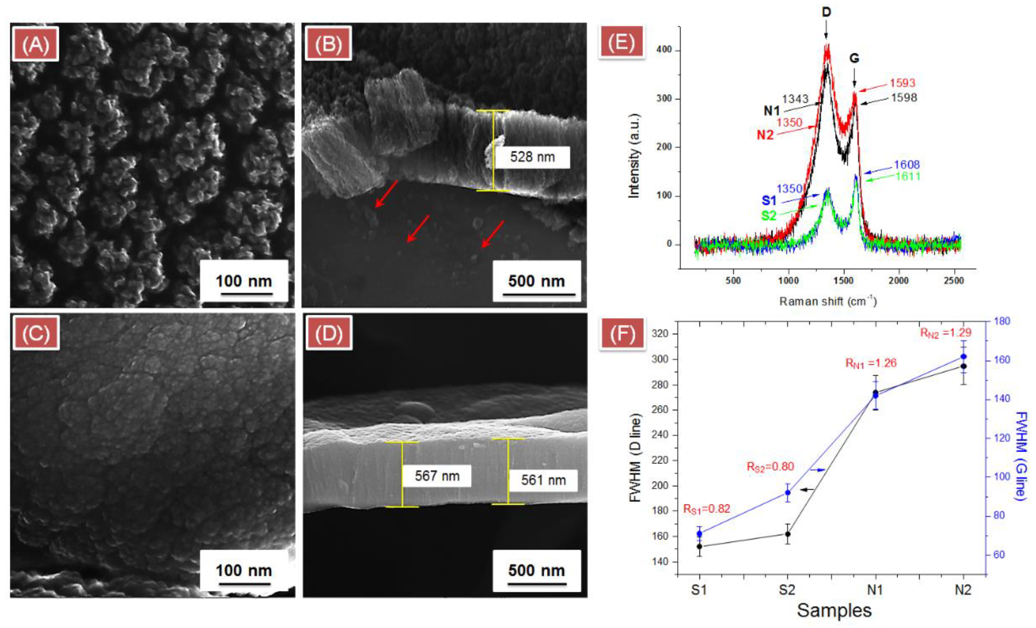
3.3. Effect of Partial Pressure of Nitrogen or Silane at Isothermal (450 °C) Conditions
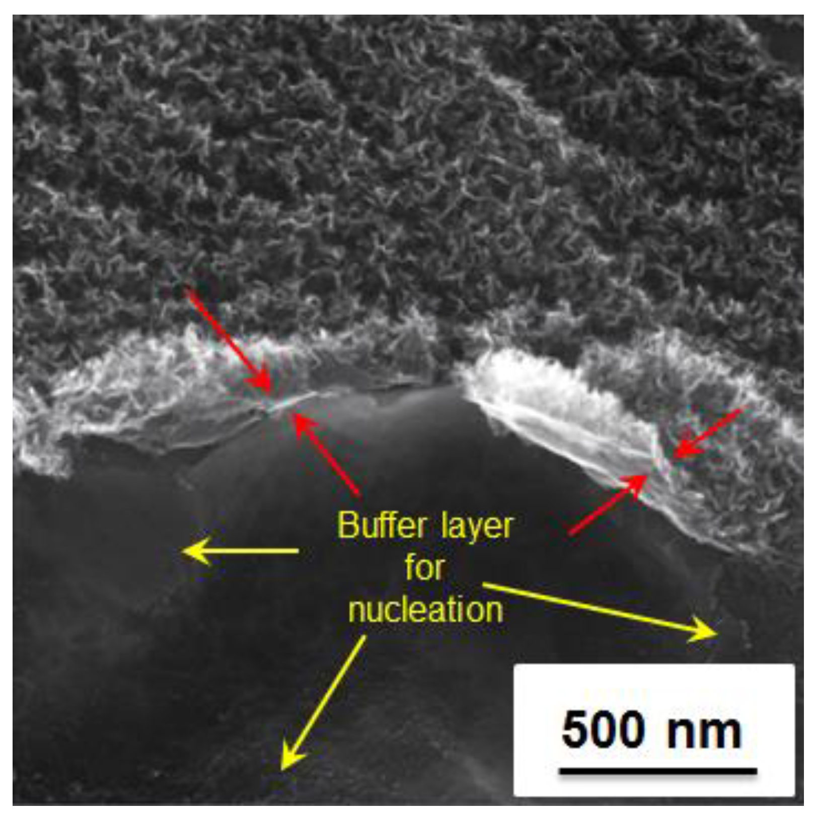
3.4. Possible Growth Mechanism of Nitrogen- or Silicon-Doped VOG
4. Conclusions
Author Contributions
Funding
Acknowledgments
Conflicts of Interest
Appendix A
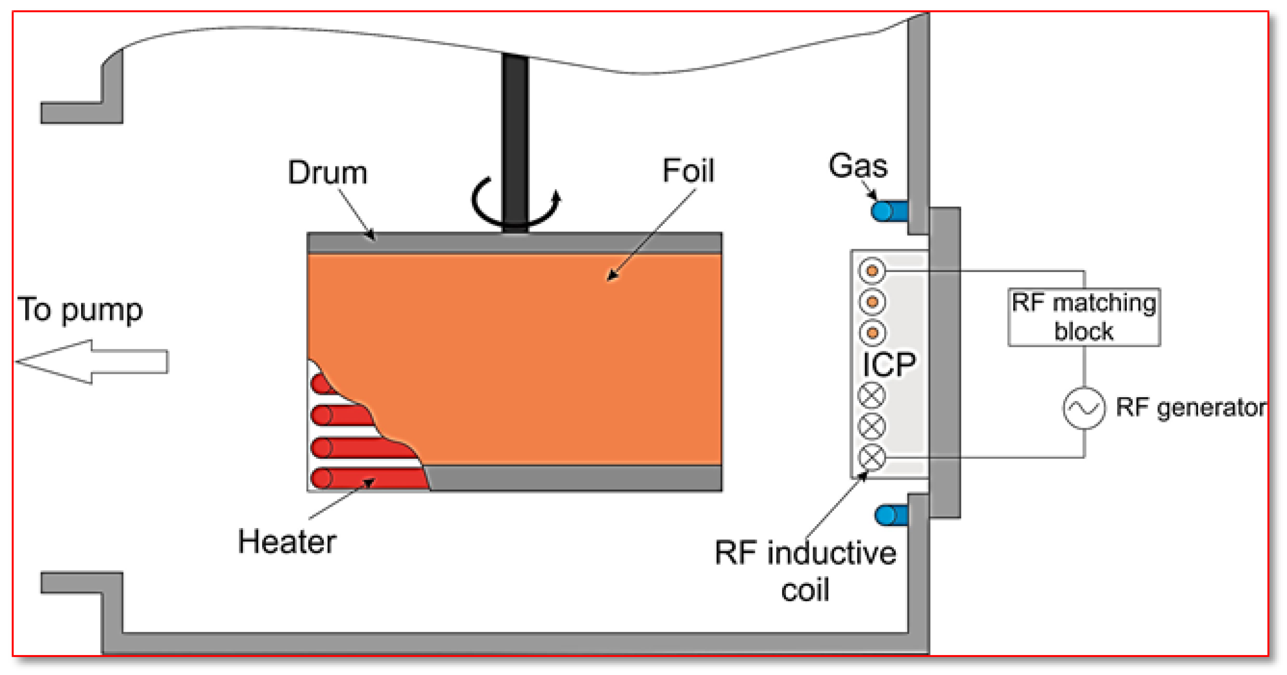
- ICP—the source of inductively coupled plasma;
- RF generator—a radio frequency signal generator to be used for the plasma process;
- RF matching block—a matching unit aiming at transmatch of output resistance of a high frequency generator with load impedance. This unit was connected to the circuit between a technological device and a transmission line of the generator.
- Gas—a gas inlet for the delivery of a gaseous mixture into the reactor interior;
- Drum—a rotating sample holder to fix the copper foil;
- Heater—a system consisting of electrodes to heat a sample to a desired temperature.


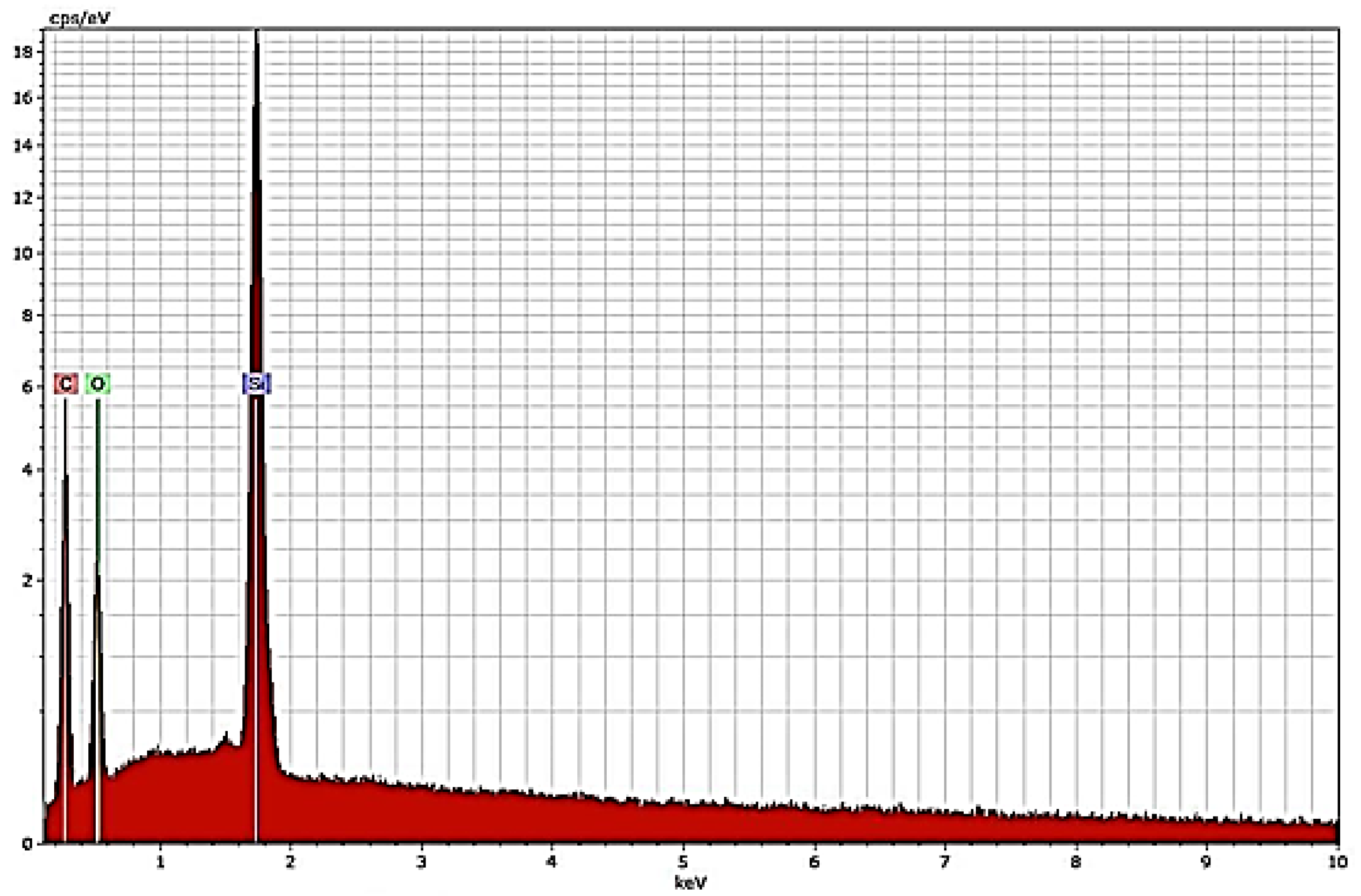
| Sample | Element | Atomic Number | Series | Norm. C [wt.%] | Atom. C [at.%] | Error [wt.%] |
|---|---|---|---|---|---|---|
| Undoped | C | 6 | K-series | 84 | 87 | 10 |
| O | 8 | K-series | 16 | 12 | 3 | |
| N1 | C | 6 | K-series | 65 | 70 | 8 |
| N | 7 | K-series | 18 | 17 | ||
| O | 8 | K-series | 15 | 13 | 3 | |
| N2 | C | 6 | K-series | 57 | 62 | 7 |
| N | 7 | K-series | 25 | 24 | 5 | |
| O | 8 | K-series | 17 | 14 | 3 | |
| S1 | C | 6 | K-series | 54 | 64 | 2 |
| O | 8 | K-series | 31 | 28 | 1 | |
| Si | 14 | K-series | 15 | 8 | 0.2 | |
| S2 | C | 6 | K-series | 48 | 63 | 7 |
| O | 8 | K-series | 19 | 19 | 3 | |
| Si | 14 | K-series | 33 | 18 | 2 |
References
- Prischepa, S.L.; Danilyuk, A.L.; Prudnikava, A.L.; Komissarov, I.V.; Labunov, V.A.; Yanushkevich, K.I.; Normand, F.L. Magnetic properties of nanocomposites based on magnetically functionalized carbon nantotubes. In Nanomagnetism; Gonzalez Estevez, J.M., Ed.; One Central Press (OCP): Cheshire, UK, 2014; pp. 227–245. [Google Scholar]
- Labunov, V.; Prudnikava, A.; Bushuk, S.; Filatov, S.; Shulitski, B.; Tay, B.K.; Shaman, Y.; Basaev, A. Femtosecond laser modification of an array of vertically aligned carbon nanotubes intercalated with Fe phase nanoparticles. Nanoscale Res. Lett. 2013, 8, 375. [Google Scholar] [CrossRef]
- Labunov, V.A.; Danilyuk, A.L.; Prudnikava, A.L.; Komissarov, I.; Shulitski, B.G.; Speisser, C.; Antoni, F.; Le, F.; Prischepa, S.L. Microwave absorption in nanocomposite material of magnetically functionalized carbon nanotubes. J. Appl. Phys. 2012, 112, 24302–241107. [Google Scholar] [CrossRef]
- Labunov, V.A.; Basaev, A.S.; Shulitski, B.G.; Shaman, Y.P.; Komissarov, I.; Prudnikava, A.L.; Tay, B.K.; Shakerzadeh, M. Growth of few-wall carbon nanotubes with narrow diameter distribution over Fe-Mo-MgO catalyst by methane/acetylene catalytic decomposition. Nanoscale Res. Lett. 2012, 7, 102. [Google Scholar] [CrossRef]
- Labunov, V.; Shulitski, B.; Prudnikava, A.; Basaev, A. Multilevel composite nanostructures based on the arrays of vertically aligned carbon nanotubes and planar graphite layers. Phys. Status Solidi 2011, 208, 453–458. [Google Scholar] [CrossRef]
- Navitski, A.; Müller, G.; Sakharuk, V.; Prudnikava, A.L.; Shulitski, B.G.; Labunov, V.A. Efficient high-current field emission from arrays of carbon nanotube columns. J. Vac. Sci. Technol. B 2010, 28, C2B14-19. [Google Scholar] [CrossRef]
- Novoselov, K.S.; Geim, A.K.; Morozov, S.V.; Jiang, D.; Zhang, Y.; Dubonos, S.V.; Grigorieva, I.V.; Firsov, A.A. Electric field effect in atomically thin carbon films. Science 2004, 306, 666–669. [Google Scholar] [CrossRef]
- Novoselov, K.S.; Jiang, D.; Schedin, F.; Booth, T.; Khotkevich, V.V.; Morozov, S.V.; Geim, A.K. Two-dimensional atomic crystals. Proc. Natl. Acad. Sci. USA 2005, 102, 10451–10453. [Google Scholar] [CrossRef] [PubMed] [Green Version]
- Bo, Z.; Mao, S.; Han, Z.J.; Cen, K.; Chen, J.; Ostrikov, K. Emerging energy and environmental applications of vertically-oriented graphenes. Chem. Soc. Rev. 2015, 44, 2108–2121. [Google Scholar] [CrossRef] [Green Version]
- Lee, H.C.; Bong, H.; Yoo, M.S.; Jo, M.; Cho, K. Copper-vapor-assisted growth and defect-healing of graphene on copper surfaces. Small 2018, 14, e1801181. [Google Scholar] [CrossRef]
- Song, Y.; Luo, Y.; Zhu, C.; Li, H.; Du, D.; Lin, Y. Recent advances in electrochemical biosensors based on graphene two-dimensional nanomaterials. Biosens. Bioelectron. 2016, 76, 195–212. [Google Scholar] [CrossRef] [PubMed]
- Torres, T. Graphene chemistry. Chem. Soc. Rev. 2017, 46, 4385–4386. [Google Scholar] [CrossRef]
- Solís-Fernández, P.; Bissett, M.; Ago, H. Synthesis, structure and applications of graphene-based 2D heterostructures. Chem. Soc. Rev. 2017, 46, 4572–4613. [Google Scholar] [CrossRef] [PubMed]
- Cho, D.; Kim, M.; Hwang, J.; Park, J.H.; Joo, Y.L.; Jeong, Y.A. Tremella-like nanostructure of silicon@void@graphene-like nanosheets composite as an anode for Lithium-ion batteries. Nanoscale Res. Lett. 2016, 11, 204. [Google Scholar] [CrossRef]
- Luo, B.; Zhi, L. Design and construction of three dimensional graphene-based composites for Lithium ion battery applications. Energy Environ. Sci. 2015, 8, 456–477. [Google Scholar] [CrossRef]
- Bundaleska, N.; Henriques, J.; Abrashev, M.; Botelho do Rego, A.M.; Ferraria, A.M.; Almeida, A.; Dias, F.M.; Valcheva, E.; Arnaudov, B.; Upadhyay, K.K.; et al. Large-scale synthesis of free-standing N-doped graphene using microwave plasma. Sci. Rep. 2018, 8, 12595. [Google Scholar] [CrossRef]
- Kong, X. Metal-free Si-doped graphene: A new and enhanced anode material for Li ion battery. J. Alloy. Compd. 2016, 687, 534–540. [Google Scholar] [CrossRef]
- Xiong, D.; Li, X.; Bai, Z.; Shan, H.; Fan, L.; Wu, C.; Li, D.; Lu, S. Superior cathode performance of nitrogen-doped graphene frameworks for Lithium ion batteries. ACS Appl. Mater. Interfaces 2017, 9, 10643–10651. [Google Scholar] [CrossRef]
- Esrafili, M.D.; Saeidi, N.; Nematollahi, P. Si-doped graphene: A promising metal-free catalyst for oxidation of SO2. Chem. Phys. Lett. 2016, 649, 37–43. [Google Scholar] [CrossRef]
- Liu, Y.; Miao, X.; Fang, J.; Zhang, X.; Chen, S.; Li, W.; Feng, W.; Chen, Y.; Wang, W.; Zhang, Y. Layered-MnO2 nanosheet grown on nitrogen-doped graphene template as a composite cathode for flexible solid-state asymmetric supercapacitor. ACS Appl. Mater. Interfaces 2016, 8, 5251–5260. [Google Scholar] [CrossRef]
- Sheng, L.; Jiang, L.; Wei, T.; Fan, Z. High volumetric energy density asymmetric supercapacitors based on well-balanced graphene and graphene-MnO2 electrodes with densely stacked architectures. Small 2016, 12, 5217–5227. [Google Scholar] [CrossRef] [PubMed]
- Xue, Y.; Wu, B.; Bao, Q.; Liu, Y. Controllable synthesis of doped graphene and its applications. Small 2014, 10, 2975–2991. [Google Scholar] [CrossRef] [PubMed]
- Komissarov, I.V.; Kovalchuk, N.G.; Labunov, V.A.; Girel, K.V.; Korolik, O.V.; Tivanov, M.S.; Lazauskas, A.; Andrulevičius, M.; Tamulevičius, T.; Grigaliūnas, V.; et al. Nitrogen-doped twisted graphene grown on copper by atmospheric pressure CVD from a decane precursor. Beilstein J. Nanotechnol. 2017, 8, 145–158. [Google Scholar] [CrossRef] [PubMed] [Green Version]
- Li, X.; Colombo, L.; Ruoff, R.S. Synthesis of graphene films on copper foils by chemical vapor deposition. Adv. Mater. 2016, 28, 6247–6252. [Google Scholar] [CrossRef]
- Fang, W.; Hsu, A.L.; Song, Y.; Kong, J. A review of large-area bilayer graphene synthesis by chemical vapor deposition. Nanoscale 2015, 7, 20335–20351. [Google Scholar] [CrossRef]
- Chen, Z.; Zhang, W.; Palma, C.-A.; Rizzini, A.L.; Liu, B.; Abbas, A.; Richter, N.; Martini, L.; Wang, X.-Y.; Cavani, N.; et al. Synthesis of graphene nanoribbons by ambient-pressure chemical vapor deposition and device integration. J. Am. Chem. Soc. 2016, 138, 15488–15496. [Google Scholar] [CrossRef] [PubMed]
- Lee, H.-C. Review of inductively coupled plasmas: Nano-applications and bistable hysteresis physics. Appl. Phys. Rev. 2018, 5, 011108. [Google Scholar] [CrossRef]
- Levchenko, I.; Ostrikov, K.; Zheng, J.; Li, X.; Keidard, M.; Teoe, K.B.K. Scalable graphene production: Perspectives and challenges of plasma applications. Nanoscale 2016, 8, 10511–10527. [Google Scholar] [CrossRef] [PubMed]
- Ye, X.; Zhou, H.; Levchenko, I.; Bazaka, K.; Xu, S.; Xiao, S. Low-temperature synthesis of graphene by ICP-Assisted amorphous carbon sputtering. ChemistrySelect 2018, 3, 8779–8785. [Google Scholar] [CrossRef]
- Zheng, S.; Zhong, G.; Wu, X.; D’Arsiè, L.; Robertson, J. Metal-catalyst-free growth of graphene on insulating substrates by ammonia-assisted microwave plasma-enhanced chemical vapor deposition. RSC Adv. 2017, 7, 33185–33193. [Google Scholar] [CrossRef] [Green Version]
- Quan, B.; Meng, Y.; Li, L.; Yao, Z.; Liu, Z.; Wang, K.; Wei, Z.; Gu, C.; Li, J. Vertical few-layer graphene/metalized Si-nanocone arrays as 3D electrodes for solid-state supercapacitors with large areal capacitance and superior rate capability. Appl. Surf. Sci. 2017, 404, 238–245. [Google Scholar] [CrossRef]
- Yivlialin, R.; Bussetti, G.; Duò, L.; Yu, F.; Galbiati, M.; Camilli, L. CVD Graphene/Ni interface evolution in sulfuric electrolyte. Langmuir 2018, 34, 3413–3419. [Google Scholar] [CrossRef] [PubMed]
- Pu, N.-W.; Shi, G.-N.; Liu, Y.-M.; Sun, X.; Chang, J.-K.; Sun, C.-L.; Ger, M.-D.; Chen, C.-Y.; Wang, P.-C.; Peng, Y.-Y.; et al. Graphene grown on stainless steel as a high-performance and ecofriendly anti-corrosion coating for polymer electrolyte membrane fuel cell bipolar plates. J. Power Sources 2015, 282, 248–256. [Google Scholar] [CrossRef]
- Ghaemi, F.; Abdullah, L.C.; Tahir, P.M.; Yunus, R. Synthesis of different layers of graphene on stainless steel using the CVD method. Nanoscale Res. Lett. 2016, 11, 506. [Google Scholar] [CrossRef] [PubMed]
- Gullapalli, H.; Reddy, A.L.M.; Kilpatrick, S.; Dubey, M.; Ajayan, P.M. Graphene growth via carburization of stainless steel and application in energy storage. Small 2011, 7, 1697–1700. [Google Scholar] [CrossRef] [PubMed]
- Shelk, M.V.; Gullapalli, H.; Kalaga, K.; Rodrigues, M.-T.F.; Devarapalli, R.R.; Vajtai, R.; Ajayan, P.M. Facile synthesis of 3D anode assembly with Si nanoparticles sealed in highly pure few layer graphene deposited on porous current collector for long life Li-Ion battery. Adv. Mater. Interfaces 2017, 4, 1601043. [Google Scholar] [CrossRef]
- Kato, R.; Minami, S.; Koga, Y.; Hasegawa, M. High growth rate chemical vapor deposition of graphene under low pressure by RF plasma assistance. Carbon 2016, 96, 1008–1013. [Google Scholar] [CrossRef]
- Manikandan, A.; Lee, L.; Wang, Y.-C.; Chen, C.-W.; Chen, Y.-Z.; Medina, H.; Tseng, J.-Y.; Wang, Z.M.; Chueh, Y.-L. Graphene-coated copper nanowire networks as a highly stable transparent electrode in harsh environments toward efficient electrocatalytic hydrogen evolution reactions. J. Mater. Chem. A 2017, 5, 13320–13328. [Google Scholar] [CrossRef]
- Griep, M.H.; Tumlin, T.M.; Smith, J.T.; Oida, S.; Sano, T.; Demaree, D.; Dimitrakopoulos, C. Enhanced quality CVD-grown graphene via a double-plateau copper surface planarization methodology. Cryst. Growth Des. 2017, 17, 5725–5731. [Google Scholar] [CrossRef]
- Ago, H.; Ohta, Y.; Hibino, H.; Yoshimura, D.; Takizawa, R.; Uchida, Y.; Tsuji, M.; Okajima, T.; Mitani, H.; Mizuno, S. Growth dynamics of single-layer graphene on epitaxial Cu surfaces. Chem. Mater. 2015, 27, 5377–5385. [Google Scholar] [CrossRef]
- Ajejas, F.; Gudín, A.; Guerrero, R.; Barcelona, A.A.; Diez, J.M.; de Melo Costa, L.; Olleros, P.; Niño, M.A.; Pizzini, S.; Vogel, J.; et al. Unraveling Dzyaloshinskii–Moriya interaction and chiral nature of graphene/cobalt interface. Nano Lett. 2018, 18, 5364–5372. [Google Scholar] [CrossRef] [PubMed]
- Zhang, D.; Xie, F.; Lin, P.; Choy, W.C.H. Al-TiO2 composite-modified single-layer graphene as an efficient transparent cathode for organic solar cells. ACS Nano 2013, 7, 1740–1747. [Google Scholar] [CrossRef]
- Verguts, K.; Vermeulen, B.; Vrancken, N.; Schouteden, K.; Van Haesendonck, C.; Huyghebaert, C.; Heyns, M.; De Gendt, S.; Brems, S. Epitaxial Al2O3(0001)/Cu(111) template development for CVD graphene growth. J. Phys. Chem. C 2016, 120, 297–304. [Google Scholar] [CrossRef]
- Nam, J.; Kim, D.-C.; Yun, H.; Shin, D.H.; Nam, S.; Lee, W.K.; Hwang, J.Y.; Lee, S.W.; Weman, H.; Kim, K.S. Chemical vapor deposition of graphene on platinum: Growth and substrate interaction. Carbon 2017, 111, 733–740. [Google Scholar] [CrossRef]
- Babenko, V.; Murdock, A.T.; Koós, A.A.; Britton, J.; Crossley, A.; Holdway, P.; Moffat, J.; Huang, J.; Alexander-Webber, J.A.; Nicholas, R.J.; et al. Rapid epitaxy-free graphene synthesis on silicidated polycrystalline platinum. Nat. Commun. 2015, 6, 7536. [Google Scholar] [CrossRef] [Green Version]
- Feng, X.; Wu, J.; Bell, A.T.; Salmeron, M. An atomic-scale view of the nucleation and growth of graphene islands on Pt surfaces. J. Phys. Chem. C 2015, 119, 7124–7129. [Google Scholar] [CrossRef]
- Li, M.; Liu, D.; Wei, D.; Song, X.; Wei, D.; Wee, A.T.S. Controllable synthesis of graphene by plasma-enhanced chemical vapor deposition and its related applications. Adv. Sci. 2016, 1600003. [Google Scholar] [CrossRef]
- Aliofkhazraei, M.; Ali, N.; Milne, W.I.; Ozkan, C.S.; Miture, S.; Gervasoni, J.L. Graphene Science Handbook: Fabrication Methods, 1st ed.; CRC Press, Taylor & Francis Group: Abingdon, UK, 2016; pp. 35–715. [Google Scholar]
- Chan, S.-H.; Chen, S.-H.; Lin, W.-T.; Li, M.-C.; Lin, Y.-C.; Kuo, C.-C. Low-temperature synthesis of graphene on Cu using plasma-assisted thermal chemical vapor deposition. Nanoscale Res. Lett. 2013, 8, 285–290. [Google Scholar] [CrossRef] [PubMed]
- Redekop, E.A.; Saerens, S.; Galvita, V.V.; González, I.P.; Sabbe, M.; Bliznuk, V.; Reyniers, M.-F.; Marin, G.B. Early stages in the formation and burning of graphene on a Pt/Mg(Al)Ox dehydrogenation catalyst: A temperature- and time-resolved study. J. Catal. 2016, 344, 482–495. [Google Scholar] [CrossRef]
- Descamps, C.; Vignoles, G.L.; Féron, O.; Langlais, F.; Lavenac, J. Correlation between homogeneous propane pyrolysis and pyrocarbon deposition. J. Electrochem. Soc. 2001, 148, C695–C708. [Google Scholar] [CrossRef]
- Wassei, J.K.; Mecklenburg, M.; Torres, J.A.; Fowler, J.D.; Regan, B.C.; Kaner, R.B.; Weiller, B.H. Chemical vapor deposition of graphene on copper from methane, ethane and propane: Evidence for bilayer selectivity. Small 2012, 8, 1415–1422. [Google Scholar] [CrossRef]
- Chen, J.; Bo, Z.; Lu, G. Vertically-Oriented Graphene, PECVD Synthesis and Applications; Springer: Cham, Switzerland, 2015. [Google Scholar] [CrossRef]
- Zhang, Z.; Lee, C.-S.; Zhang, W. Vertically aligned graphene nanosheet arrays: Synthesis, properties and applications in electrochemical energy conversion and storage. Adv. Energy Mater. 2017, 7, 1700678. [Google Scholar] [CrossRef]
- Wei, D.; Peng, L.; Li, M.; Mao, H.; Niu, T.; Han, C.; Chen, W.; Wee, A.T.S. Low temperature critical growth of high quality nitrogen doped graphene on dielectrics by plasma-enhanced chemical vapor deposition. ACS Nano 2015, 9, 164–171. [Google Scholar] [CrossRef] [PubMed]
- Seo, D.H.; Kumar, S.; Rider, A.E.; Han, Z.; Ostrikov, K. Deterministic control of structural and optical properties of plasma-grown vertical graphene nanosheet networks via nitrogen gas variation. Opt. Mater. Express 2012, 2, 700–707. [Google Scholar] [CrossRef]
- Luo, B.; Whelan, P.R.; Shivayogimath, A.; Mackenzie, D.M.A.; Bøggild, P.; Booth, T.J. Copper oxidation through nucleation sites of chemical vapor deposited graphene. Chem. Mater. 2016, 28, 3789–3795. [Google Scholar] [CrossRef]
- Li, P.; Li, Z.; Yang, J. Dominant kinetic pathways of graphene growth in chemical vapor deposition: The role of hydrogen. J. Phys. Chem. C 2017, 121, 25949–25955. [Google Scholar] [CrossRef]
- Wang, X.; Sun, G.; Routh, P.; Kim, D.-H.; Huang, W.; Chen, P. Heteroatom-doped graphene materials: Syntheses, properties and applications. Chem. Soc. Rev. 2014, 43, 7067–7098. [Google Scholar] [CrossRef] [PubMed]
- Pham, P.V. A Library of doped-graphene images via transmission electron microscopy. J. Carbon Res. 2018, 4, 34. [Google Scholar] [CrossRef]
- Chen, Y.; Liu, Y.-J.; Wang, H.-X.; Zhao, J.-X.; Cai, Q.-H.; Wang, X.-Z.; Ding, Y.-H. Silicon-doped graphene: AN effective and metal-free catalyst for NO reduction to N2O? ACS Appl. Mater. Interfaces 2013, 5, 5994–6000. [Google Scholar] [CrossRef]
- Wang, H.; Zhou, Y.; Wu, D.; Liao, L.; Zhao, S.L.; Peng, H.L.; Liu, Z.F. Synthesis of boron-doped graphene monolayers using the sole solid feedstock by chemical vapor deposition. Small 2013, 9, 1316–1320. [Google Scholar] [CrossRef] [PubMed]
- Peyghan, A.A.; Rastegar, S.F.; Hadipour, N.L. DFT study of NH3 adsorption on pristine, Ni-and Si-doped graphynes. Phys. Lett. A 2014, 378, 2184–2190. [Google Scholar] [CrossRef]
- Lv, R.; dos Santos, M.C.; Antonelli, C.; Feng, S.; Fujisawa, K.; Berkdemir, A.; Cruz-Silva, R.; Elías, A.L.; Perea-Lopez, N.; López-Urías, F.; et al. Large-area Si-doped graphene: Controllable synthesis and enhanced molecular sensing. Adv. Mater. 2014, 26, 7593–7599. [Google Scholar] [CrossRef]
- Wang, Z.; Li, P.; Chen, Y.; Liu, J.; Zhang, W.; Guo, Z.; Dong, M.; Li, Y. Synthesis, characterization and electrical properties of silicon-doped graphene films. J. Mater. Chem. C 2015, 3, 6301–6306. [Google Scholar] [CrossRef]
- Cuxart, M.G.; Šics, I.; Goñi, A.R.; Pach, E.; Sauthier, G.; Paradinas, M.; Foerster, M.; Aballe, L.; Fernandez, H.M.; Carlino, V.; Pellegrin, E. Inductively coupled remote plasma-enhanced chemical vapor deposition (rPE-CVD) as a versatile route for the deposition of graphene micro- and nanostructures. Carbon 2017, 117, 331–342. [Google Scholar] [CrossRef] [Green Version]
- Chen, J.; Bo, Z.; Lu, G. PECVD Synthesis of Vertically-Oriented Graphene: Precursor and Temperature Effects. In Vertically Oriented Graphene; ebook; Springer: Cham, Switzerland, 2015; pp. 35–54. [Google Scholar] [CrossRef]
- Naghdi, S.; Rhee, K.Y.; Park, S.J. A catalytic, catalyst-free, and Roll-to-Roll production of graphene via chemical vapor deposition: Low temperature growth. Carbon 2018, 127, 1–12. [Google Scholar] [CrossRef]
- Cançado, L.; Takai, K.; Enoki, T.; Endo, M.; Kim, Y.A.; Mizusaki, H.; Jorio, A.; Coelho, L.N.; Magalhães-Paniago, R.; Pimenta, M.A. General equation for the determination of the crystallite size La of nanographite by Raman spectroscopy. Appl. Phys. Lett. 2006, 88, 163106. [Google Scholar] [CrossRef]
- Li, X.; Cai, W.; An, J.; Kim, S.; Nah, J.; Yang, D.; Piner, R.; Velamakanni, A.; Jung, I.; Tutuc, E.; et al. Large-area synthesis of high-quality and uniform graphene films on copper foils. Science 2009, 324, 1312–1314. [Google Scholar] [CrossRef]
- Levine, M.S.; Golovin, A.A.; Volpert, V.A. Step-flow growth of a crystal surface by Lévy flights. Eur. Phys. Lett. 2008, 82, 28007. [Google Scholar] [CrossRef]
- Yakobson, B.I.; Brabec, C.J.; Bernholc, J. Nanomechanics of carbon tubes: Instabilities beyond linear response. Phys. Rev. Lett. 1996, 76, 2511–2514. [Google Scholar] [CrossRef]
- Cançado, L.G.; Jorio, A.; Ferreira, E.H.M.; Stavale, F.; Achete, C.A.; Capaz, R.B.; Moutinho, M.V.O.; Lombardo, A.; Kulmala, T.S.; Ferrari, A.C. Quantifying defects in graphene via Raman spectroscopy at different excitation energies. Nano Lett. 2011, 11, 3190–3196. [Google Scholar] [CrossRef] [PubMed]
- Ferreira, E.H.M.; Moutinho, M.V.O.; Stavale, F.; Lucchese, M.M.; Capaz, R.B.; Achete, C.A.; Jorio, A. Evolution of the Raman spectra from single-, few-, and many-layer graphene with increasing disorder. Phys. Rev. B 2010, 82, 125429. [Google Scholar] [CrossRef]
- Ferrari, A.C.; Robertson, J. Interpretation of Raman spectra of disordered and amorphous carbon. Phys. Rev. B 2000, 61, 14095–14107. [Google Scholar] [CrossRef]
- Ferrari, A.C. Raman spectroscopy of graphene and graphite: Disorder, electron-phonon coupling, doping and nonadiabatic effects. Solid State Commun. 2007, 143, 47–57. [Google Scholar] [CrossRef]
- Woehrl, N.; Ochedowski, O.; Gottlieb, S.; Shibasaki, K.; Schulz, S. Plasma-enhanced chemical vapor deposition of graphene on copper substrates. AIP Adv. 2014, 4, 047128. [Google Scholar] [CrossRef] [Green Version]
- Muhl, S.; Méndez, J.M. A Review of the preparation of carbon nitride film. Diam. Relat. Mater. 1999, 8, 1809–1830. [Google Scholar] [CrossRef]
- Chakradhar, A.; Sivapragasam, N.; Nayakasinghe, M.T.; Burghaus, U. Support effects in the adsorption of water on CVD graphene: An ultra-high vacuum adsorption study. Chem. Commun. 2015, 51, 11463–11466. [Google Scholar] [CrossRef] [PubMed]
- Chen, Y.; Yang, X.-C.; Liu, Y.-J.; Zhao, J.-X.; Cai, Q.-H.; Wang, X.-Z. Can Si-doped graphene activate or dissociate O2 molecule? J. Mol. Gr. Model. 2013, 39, 126–132. [Google Scholar] [CrossRef] [PubMed]
- Ellingham, H.J.T. Reproducibility of oxides and sulphides in metallurgical processes. J. Soc. Chem. Ind. 1944, 63, 125–133. [Google Scholar]
- Luo, Z.; Yu, T.; Shang, J.; Wang, Y.; Lim, S.; Liu, L.; Gurzadyan, G.G.; Shen, Z.; Lin, J. Large-scale synthesis of bi-layer graphene in strongly coupled stacking order. Adv. Funct. Mater. 2011, 21, 911–917. [Google Scholar] [CrossRef]
- Kuper, C.A.; Labes, M.M. A new method of doping pyrolytic graphite utilizing laser heating in the presence of organic heteroatomic vapors. Chem. Mater. 1999, 11, 408–411. [Google Scholar] [CrossRef]
- Marton, D.; Boyd, K.J.; Al-Bayati, A.H.; Todorov, S.S.; Rabalais, J.W. Carbon nitride deposited using energetic species: A two-phase system. Phys. Rev. Lett. 1994, 73, 118–121. [Google Scholar] [CrossRef]
- Dresselhaus, S.; Dresselhaus, G.; Avouris, P. Carbon Nanotubes: Synthesis, Structure, Properties, and Applications, 1st ed.; Springer: Berlin/Heidelberg, Germany, 2001; pp. 1–448. [Google Scholar] [CrossRef]
- Ripalda, J.M.; Montero, I.; Galán, L. An XPS study of carbon nitride synthesized by ion beam nitridation of C60 fullerene. Diam. Relat. Mater. 1998, 7, 402–406. [Google Scholar] [CrossRef]
- Hellgren, N.; Johansson, M.P.; Broitman, E.; Hultman, L.; Sundgren, J.-E. Role of nitrogen in the formation of hard and elastic CNx thin films by reactive magnetron sputtering. Phys. Rev. B 1999, 59, 5162–5169. [Google Scholar] [CrossRef]
- Ronning, C.; Feldermann, H.; Merk, R.; Hofsäss, H.; Reinke, P.; Thiele, J.-U. Carbon nitride deposited using energetic species: A review on XPS studies. Phys. Rev. B 1998, 58, 2207–2215. [Google Scholar] [CrossRef]
- Liu, A.Y.; Cohen, M.L. Prediction of new low compressibility solids. Science 1989, 245, 841–842. [Google Scholar] [CrossRef] [PubMed]
- Wu, P.; Du, P.; Zhang, H.; Cai, C. Microscopic effects of the bonding configuration of nitrogen-doped graphene on its reactivity toward hydrogen peroxide reduction reaction. Phys. Chem. Chem. Phys. 2013, 15, 6920–6928. [Google Scholar] [CrossRef]
- Sjöström, H.; Stafström, S.; Boman, M.; Sundgren, J.-E. Superhard and Elastic Carbon Nitride Thin Films Having Fullerenelike Microstructure. Phys. Rev. Lett. 1995, 75, 1336–1339. [Google Scholar] [CrossRef]
- Shamir, N.; Baldwin, D.A.; Darko, T.; Rabalais, J.W.; Hochmann, P. Reactions of homonuclear diatomic ions with metal surfaces. II. Nitridation of Al, Cu, Mo, and Ni by N2+ beams in the low kinetic energy-near threshold region. J. Chem. Phys. 1982, 76, 6417–6424. [Google Scholar] [CrossRef]
- Li, X.; Magnuson, C.W.; Venugopal, A.; An, J.; Suk, J.W.; Han, B.; Borysiak, M.; Cai, W.; Velamakanni, A.; Zhu, Y.; et al. Graphene films with large domain size by a two-step chemical vapor deposition process. Nano Lett. 2010, 10, 4328–4334. [Google Scholar] [CrossRef]
- Wofford, J.M.; Nie, S.; McCarty, K.F.; Bartelt, N.C.; Dubon, O.D. Graphene islands on Cu foils: The interplay between shape, orientation, and defects. Nano Lett. 2010, 10, 4890–4896. [Google Scholar] [CrossRef] [PubMed]
- Zhao, J.; Shaygan, M.; Eckert, J.; Meyyappan, M.; Rümmeli, M.H. A growth mechanism for free-standing vertical graphene. Nano Lett. 2014, 14, 3064–3071. [Google Scholar] [CrossRef] [PubMed]
- Zhao, X.; Outlaw, R.A.; Wang, J.J.; Zhu, M.Y.; Smith, G.D.; Holloway, B.C. Thermal desorption of hydrogen from carbon nanosheets. J. Chem. Phys. 2006, 124, 194704. [Google Scholar] [CrossRef] [PubMed]
- Wood, J.D.; Schmucker, S.W.; Lyons, A.S.; Pop, E.; Lyding, J.W. Effects of polycrystalline Cu substrate on graphene growth by chemical vapor deposition. Nano Lett. 2011, 11, 4547–4554. [Google Scholar] [CrossRef] [PubMed]
- Hao, Y.; Bharathi, M.S.; Wang, L.; Liu, Y.; Chen, H.; Nie, S.; Wang, X.; Chou, H.; Tan, C.; Fallahazad, B.; et al. The Role of surface oxygen in the growth of large single-crystal graphene on copper. Science 2013, 342, 720–723. [Google Scholar] [CrossRef] [PubMed]


| Sample | Deposition Time, min | Heating Time (min)/T (°C) | Pressure (+Ar), Pa | C3H8, sccm | N2, Pa | SiH4, sccm |
|---|---|---|---|---|---|---|
| 1 | 1 | 40/450 | 1 | 200 | – | – |
| 2 | 5 | 40/450 | 1 | 200 | – | – |
| 3 | 10 | 40/450 | 1 | 200 | – | – |
| 4 | 15 | 40/450 | 1 | 200 | – | – |
| 5 | 30 | 40/450 | 1 | 200 | – | – |
| 6 | 5 | 40/450 | 0.8 | 50 | – | – |
| 7 | 10 | 20/350 | 1 | 200 | – | – |
| 8 | 10 | 60/500 | 1 | 200 | – | – |
| 9 | 10 | 40/450 | 1.4 | 400 | – | – |
| N1 | 10 | 45/450 | 1 | 200 | 0.5 | – |
| N2 | 10 | 45/450 | 1.5 | 200 | 1 | – |
| S1 | 10 | 45/450 | 1.5 | 200 | – | 50 |
| S2 | 10 | 45/450 | 1.5 | 200 | – | 100 |
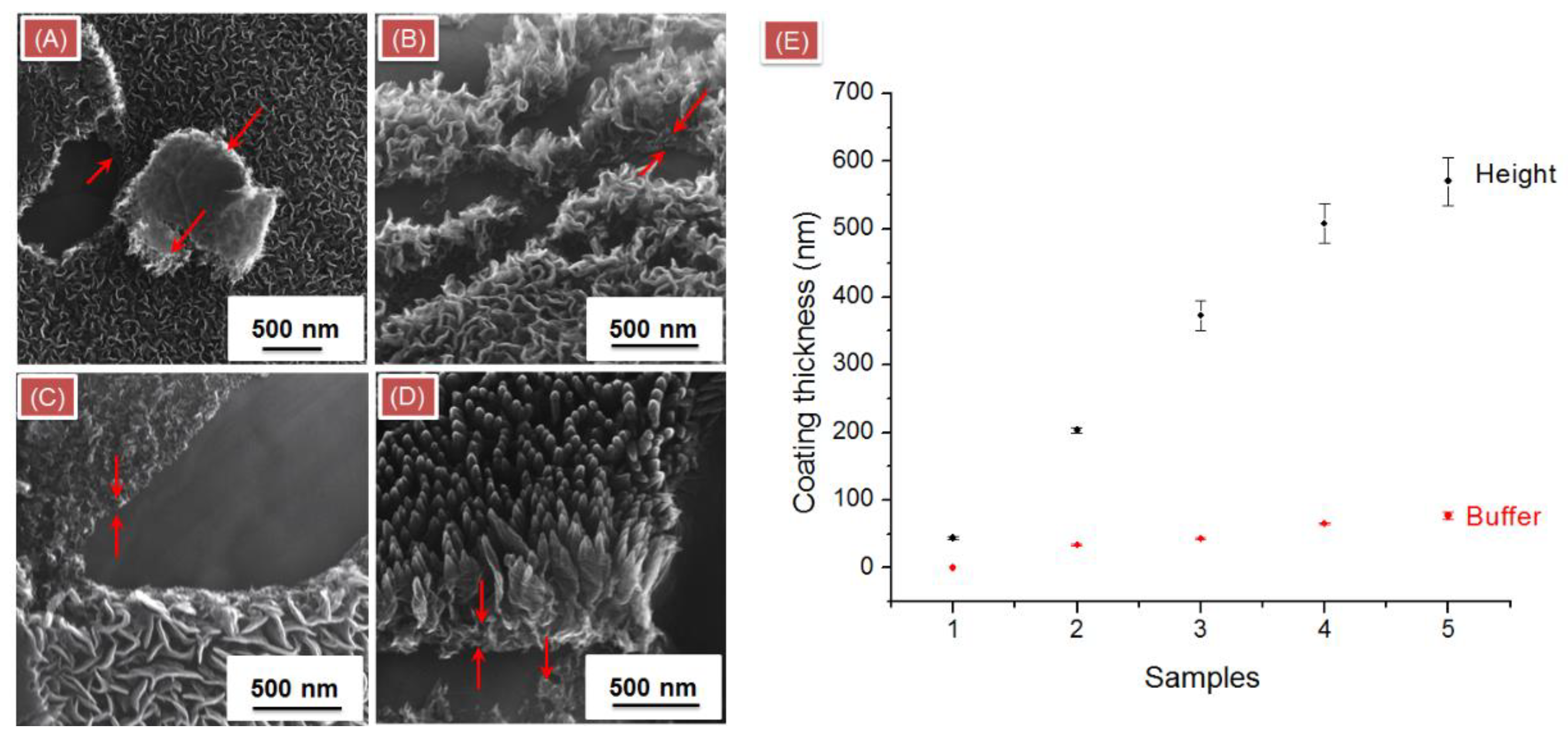
| Sample | Height of Coating, nm | Height of Buffer Layer, nm |
|---|---|---|
| 1 | 44 ± 3 | N/A |
| 2 | 203 ± 4 | 34 ± 2 |
| 3 | 373 ± 22 | 43 ± 2 |
| 4 | 508 ± 29 | 65 ± 2 |
| 5 | 570 ± 36 | 77 ± 6 |
| 6 | 189 ± 3 | 42 ± 3 |
| 7 | 318 ± 5 | 22 ± 2 |
| 8 | 308 ± 7 | 63 ± 5 |
| 9 | 489 ± 6 | N/A |
| N1 | 489 ± 6 | N/A |
| N2 | 528 ± 8 | N/A |
| S1 | 497 ± 22 | N/A |
| S2 | 564 ± 3 | N/A |
© 2019 by the authors. Licensee MDPI, Basel, Switzerland. This article is an open access article distributed under the terms and conditions of the Creative Commons Attribution (CC BY) license (http://creativecommons.org/licenses/by/4.0/).
Share and Cite
Rozel, P.; Radziuk, D.; Mikhnavets, L.; Khokhlov, E.; Shiripov, V.; Matolínová, I.; Matolín, V.; Basaev, A.; Kargin, N.; Labunov, V. Properties of Nitrogen/Silicon Doped Vertically Oriented Graphene Produced by ICP CVD Roll-to-Roll Technology. Coatings 2019, 9, 60. https://doi.org/10.3390/coatings9010060
Rozel P, Radziuk D, Mikhnavets L, Khokhlov E, Shiripov V, Matolínová I, Matolín V, Basaev A, Kargin N, Labunov V. Properties of Nitrogen/Silicon Doped Vertically Oriented Graphene Produced by ICP CVD Roll-to-Roll Technology. Coatings. 2019; 9(1):60. https://doi.org/10.3390/coatings9010060
Chicago/Turabian StyleRozel, Petr, Darya Radziuk, Lubov Mikhnavets, Evgenij Khokhlov, Vladimir Shiripov, Iva Matolínová, Vladimír Matolín, Alexander Basaev, Nikolay Kargin, and Vladimir Labunov. 2019. "Properties of Nitrogen/Silicon Doped Vertically Oriented Graphene Produced by ICP CVD Roll-to-Roll Technology" Coatings 9, no. 1: 60. https://doi.org/10.3390/coatings9010060