1. Introduction
Well before the age of dedicated scientific inquiry and technological innovation, metal-smiths of the ancient world made use of metal thin films to gild less-precious materials in thin layers of gold and silver [
1]. Although these craftsmen were likely ignorant of the physicochemical processes involved in their plating procedures, their contributions to metal film deposition techniques have inspired centuries of thin film innovation for applications that extend far beyond their mere artistic origins. Building on that foundation, modern metal thin films are utilized in a variety of scientific and industrial applications, but few more so than in the field of optics. Such films offer an uncommon combination of transparency and conductivity for certain compositions and thicknesses, while also boasting broadband reflectivity for relatively thicker films [
2,
3].
Depending on the desired film characteristics, a variety of different metals have been utilized in thin film optics, employing both pure metal films and metal-containing composites, such as Indium Tin Oxide (ITO), with applications ranging from optoelectronics to surface plasmon generation, examples of which are provided in
Table 1 with references for the interested reader. Amongst the more common of these applications, metal films are often deposited in nanoscale thicknesses on ceramic substrates in order to create high-quality broadband mirrored surfaces. Such mirrors have been utilized in reflecting telescopes as alternatives to lens arrays in order to reduce image aberrations, in microscopy for dark-field illumination, or in adaptive optics to create deformable mirrors for optical wavefront control [
4,
5,
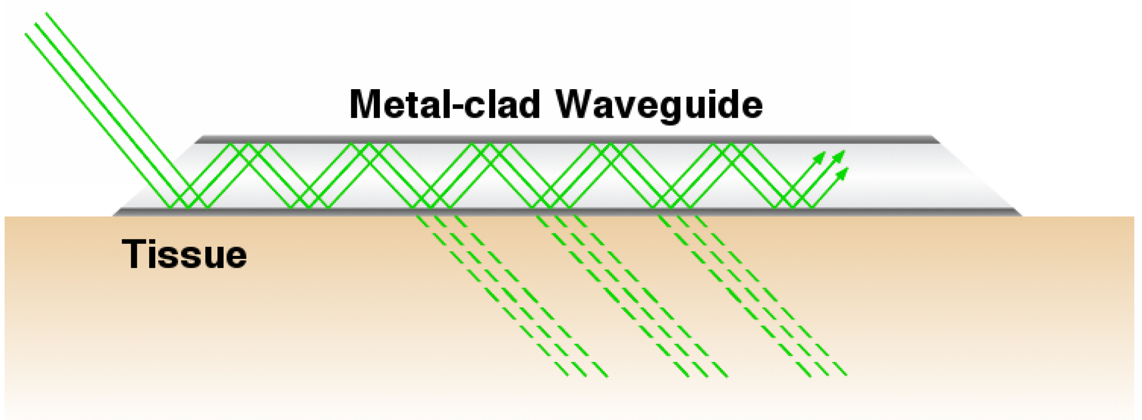
6]. Such high quality mirrors are also widely used in laser applications to exert control over laser beam directionality and propagation. For example, in the field of biophotonics, of particular interest to this work, articulated mirror arms are utilized in clinical laser dermatology systems to redirect high-powered, short-pulsed laser light toward the clinical target; meanwhile, metal film-clad optical waveguides are also being developed for direct-contact coupling of laser light into tissue via optical tunneling, as depicted in
Figure 1 [
7,
8,
9,
10].
Many contemporary laser systems also make use of metal thin films throughout their optical train, whether involved in the generation of the beam within the lasing medium or the redirection of the beam toward the desired target. For example, in the case of solid lasing media (e.g., Nd:YAG crystals), it is sometimes sufficient to simply polish the opposing ends of the material to an optical grade finish in order to achieve the lasing action; however, for higher power applications, like medical laser ablation, the ends of the medium are often also coated with a highly reflective metal film in order to generate a beam of consistent intensity [
18]. In such cases, the facets of the material will be polished to an extreme degree of flatness and parallelism prior to being coated with a thin layer of metal; typically aluminum or silver. In order to allow the beam to escape confinement within the lasing medium, however, one of the metal film mirrors must be partially transmissive.
1.1. Importance of Film Thickness in Optics
The performance of these mirrors in their respective applications is largely dependent on three principal factors: the wavelength of light being used, the optical properties of the metal film and the film’s thickness. Of these three, however, the wavelength of light is typically both fixed and known, particularly for laser-related applications. Additionally, the optical properties of standard metals—including absorption, reflectivity and refractive index—have been extensively researched and are available in established databases [
19]. Consequently, in any given application, with wavelength and film composition appropriately chosen beforehand, the film’s thickness will have the greatest effect on its performance characteristics. Therefore, by varying the film thickness, often only by tens of nanometers, the degree to which each of the bulk physical and optical properties is expressed may be tailored in order to achieve the wide variety of effects listed in
Table 1. However, it should be noted that the characteristics of the film deposition process can exhibit significant effects on the film’s optical properties, particularly for thinner films. For example, Kemmenoe et al. demonstrated that when sputter coating thin films of gold, ion beam sputter coating yielded relatively large grain sizes for films less than 10 nm thick, but that beyond that thickness, the grains amalgamate into a homogenous film [
20]. Such inhomogeneities may impact the film’s optical properties due to grain boundary interface scattering of free carriers. Moreover, although optical properties of thin metal films tend toward those of the bulk material with increasing thickness, the chosen thin film fabrication process may impact whether bulk properties are ever truly reached [
21].
For the purposes of this review, the aforementioned application involving metal film-clad optical waveguides, shown in
Figure 1, serves as a specific example to demonstrate the significance of accurately controlling and characterizing film thickness in order to tailor the performance characteristics of the waveguide. The waveguides are designed to transmit light directly into the tissue by means of an evanescent-leaking effect referred to as optical tunneling. This application sees the use of glass slab substrates as optical light guides that are designed to restrict the propagation of the visible laser light within their bounding surfaces, specifically 532 nm from a Q-switched Nd:YAG laser. The substrates are clad in thin films of titanium and silver with a total thickness on the order of 200 nm. Using thin films of metal as a cladding layer guarantees that the waveguides can operate throughout a range of internal reflection angles from 6
90
, which can be directly calculated using Snell’s law [
8,
22,
23,
24].
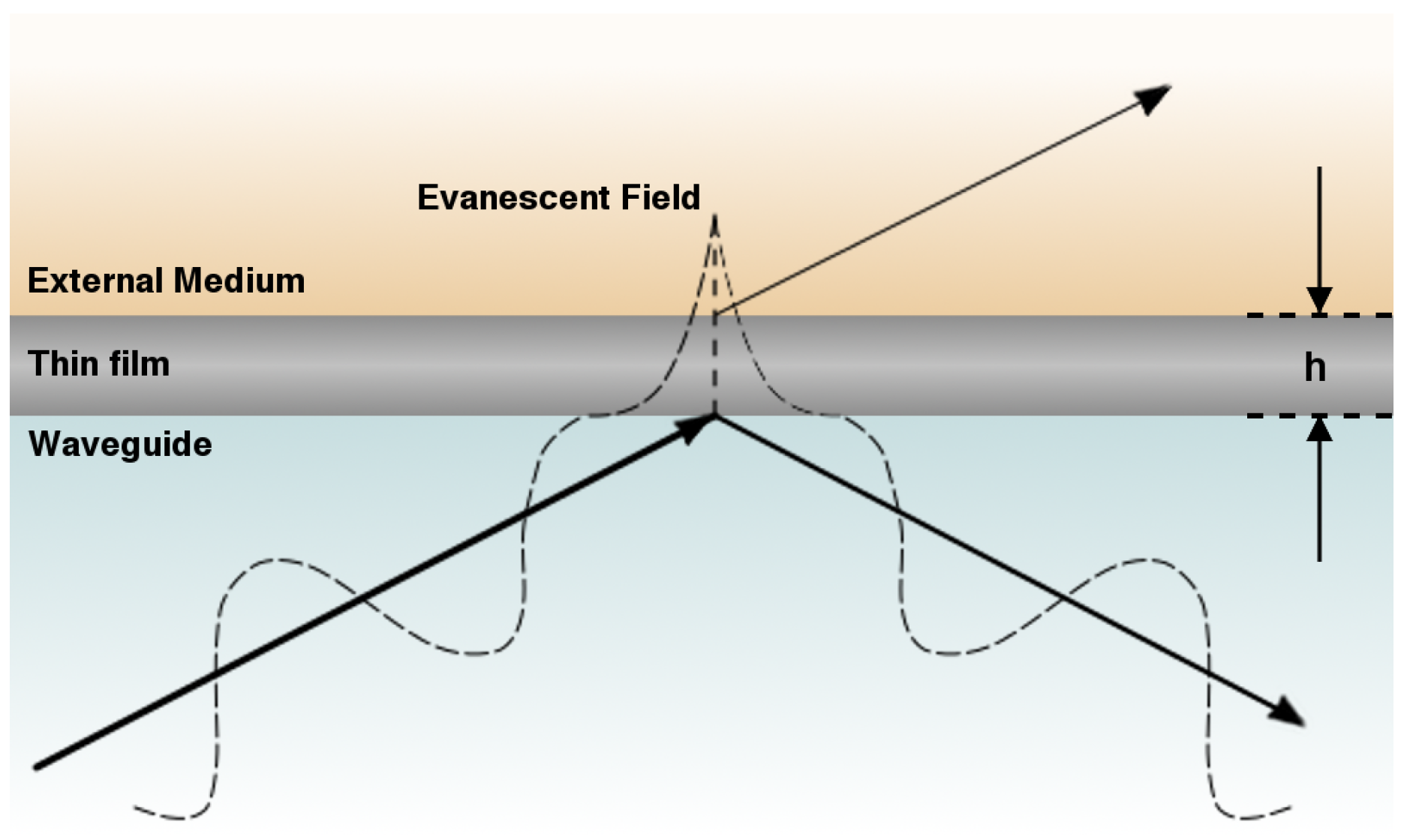
The waveguides are designed such that the light will reflect within the parallel silver films until reaching an “active area”, wherein the silver film’s thickness is much thinner, between 0 and 30 nm, and the light is capable of escaping confinement through optical tunneling, which is comparable to the quantum tunneling experienced by electrons under similar situations. As the laser interacts with the glass-metal interface, a portion of the incident photons within the glass will penetrate into the external medium in the form of an exponentially decaying electromagnetic field, referred to as the evanescent field [
25,
26].
Figure 2 demonstrates that in situations wherein the film thickness is shorter than the penetration depth of this field, the peak of the field may protrude through the film and interact with the third external medium. Under such circumstances, the protruding peak may revert back into a propagating field and refract into the tertiary medium, having “optically tunneled” through the metal film [
27]. This optical tunneling is utilized in the waveguide application to transmit the laser light into tissue that is in direct contact with the waveguide.
The importance of the silver film thickness in this case relates to the degree to which optical tunneling occurs, as the effect is proportional to the extent to which the evanescent peak protrudes into the external medium, which is correlated to the refractive index and thickness of the cladding film. It has been demonstrated that regulating the thickness of the metal film along the waveguide and within the active area affords control over the location and intensity of energy transmission into the tissue [
9]. Consequently, for this example, the accurate characterization of the metal film’s thickness is of paramount importance in appropriately exerting control over the beam propagation, both for maintaining confinement within the waveguide and for transmitting the light into the external medium.
1.2. Metal Thin Film Characterization
Such concerns reverberate throughout the field of metal thin film optics, as the thickness clearly plays such an important role in determining the efficacy of each technology. For the metal clad waveguides, the film thickness determines the degree of transmission into the external medium; whereas for applications in other fields, as in optoelectronics, the film thickness has significant ramifications on conductivity, resistivity and bulk optical absorption, as well. However, the majority of metal thin films are deposited in thicknesses much shorter than the wavelength of visible light and, as such, are well beyond the diffraction limit of traditional microscopy.
In certain applications, obtaining an estimate of the film thickness within ±50 nm may be sufficient, particularly if the intention is akin to simple mirror fabrication, wherein the principal property of concern is bulk reflectivity. In such cases, older, less complex techniques may be utilized to obtain a functional approximation of the film thickness. Amongst the oldest and most established characterization techniques, UV-Vis spectrophotometry provides a relatively quick and simple analysis of material optical properties, from which bulk film properties can be discerned. Although this technique does not provide the nanoscale resolution offered by other more advanced methods, it is one of the simplest and least expensive characterization methods and can often provide a general measurement of film transmissivity and reflectivity, from which the film thickness may be derived [
28]. However, the technique is largely subject to measurement errors and assumptions made in fitting the theoretical equations to the measured interference spectra, resulting in film thickness measurements that may be as much as 200 nm disparate from measurements produced by more reliable techniques, such as ellipsometry [
28,
29].
Consequently, a variety of alternative methods have been established for determining film thickness to a much greater degree of accuracy. It is therefore the purpose of this review to present some of the most predominant characterization methods with respect to their functional theory, methods and data analysis procedures. This article is intended to serve as a brief introduction to each of the most prominent techniques, while highlighting their individual limitations and considerations with regard specifically to the characterizing of metal thin films. In the sections that follow, we provide a cursory introduction to each X-ray Reflectivity (XRR), Ellipsometry, Atomic Force Microscopy (AFM), cross-sectional Scanning Electron Microscopy (SEM) and SEM coupled with Energy-Dispersive X-ray Spectroscopy (SEM/EDS).
2. Established Characterization Techniques
Thin film characterization has long been plagued by the limitations of optical microscopy and contemporary electronics. Although the films themselves have been in consistent use for centuries, their chemical structure and physical geometry had been largely a mystery until the relatively recent development of electronic imaging technologies, albeit many of the original limitations still apply. Nevertheless, the ability to measure and image beyond the diffraction limit of visible light has dramatically improved our understanding of thin film geometry and our capability to closely control thin film fabrication. The sections that follow introduce each of the four aforementioned thin film characterization techniques, covering their respective theories, methods and analytical methods individually before discussing their principal concerns and restrictions collectively.
Table 2 lists additional techniques not discussed herein, their most relevant considerations and limitations, vertical resolutions and accompanying references for the interested reader. It should be noted that the thickness range of any chosen technique will be predominately dependent on the make, model and manufacturer of the equipment in question; readers are advised to contact the manufacturer to obtain equipment specifications.
2.1. X-ray Reflectivity
The first of the primary technologies used in thin film material characterization, X-ray Reflectivity (XRR), operates in a similar manner to UV-Vis reflectance spectrophotometry, with the principal difference that the photons emitted and measured are of substantially shorter wavelengths and higher frequency than those in the UV and visible spectra. The use of X-ray photons instead of visible spectrum radiation allows measurement to circumvent inaccuracies caused by the optical absorption of visible light while also allowing decreasing of the effective diffraction limit. Additionally, whereas traditional spectrophotometry suffers inaccuracies when the observed spectrum deviates from the theoretically-expected curve, X-ray reflectivity relies entirely on the deviation from theory in order to derive material properties. The subsections that follow introduce the operational theory and general apparatus design of XRR before discussing the procedure for data analysis and thickness derivation.
2.1.1. XRR: Theory
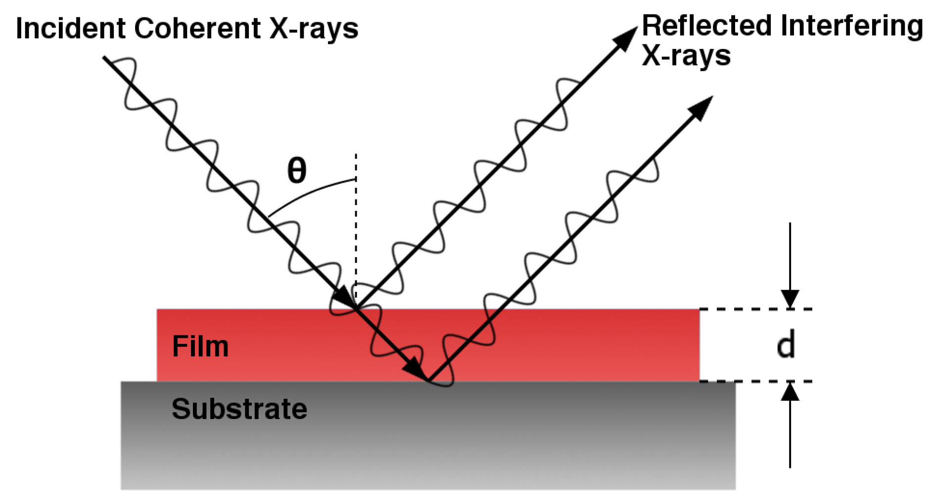
With regard to the operational theory, XRR builds on some of the same fundamental optical theories that gave rise to UV-Vis spectrophotometry. In traditional reflectance spectrophotometry, incident light reflects off the interface between the thin film and the air and again off the interface between the film and the substrate (or the next intermediary layer), forming interference patterns by scanning the sample throughout a range of incident wavelengths. By contrast, X-ray reflectivity functions by scanning the sample surface with a monochromatic beam of X-ray photons throughout a range of incident angles . Although the wavelength of the incident photons does not change, the changing incident angle results in variations in the amplitude of the reflected beam, which generates interference patterns throughout the angular spectrum.
Research has demonstrated that typically, the most relevant and useful data will be recorded within a few degrees of the critical angle between the sample and the surrounding atmosphere. Seeing as the same optical principles may be applied to X-ray photons as to visible radiation, the critical angle can be calculated from the simplified form of Snell’s law:
given that the sample medium is less optically dense than the surrounding medium at the X-ray wavelength (i.e.,
) [
49]. As with visible optics, angles of incidence less than
will result in a portion of the incident beam refracting into the medium, while the remaining portion of the beam reflects away; whereas angles greater than
will result in the incident beam totally reflecting away from the interface. Consequently, scanning through the range of angles surrounding the critical angle yields multiple beam scenarios, such as are depicted in
Figure 3.
However, the true strength of the technique is derived from the extremely short wavelengths of X-ray photons, which permits them to interact with materials on an atomic level. As a result, the incident beam is strongly susceptible to the changes in electron density that occur at the interfaces between the media of differing refractive indices, due to the strong dependence of the refractive index on electron density. As the incident angle changes, the X-rays reflecting off the surface will interfere with the X-rays that penetrate the sample and reflect off the sample-substrate interface. This interference results in constructive and destructive peaks and valleys in the measured spectra. Therefore, by recording the amplitude of the specularly-reflected X-rays and their coherence, a parameterized model can be fit to the data to incorporate electron density
, thickness
d and surface roughness
r. Although the parameterized model can reveal more specific information about the sample, a quick analysis reveals that the periodicity of the peaks is proportional to
, whereas the amplitude is proportional to the density difference [
49]. Moreover, more complex models can be implemented for cases involving multilayered structures, such as the fused silica-titanium-silver multilayered waveguides discussed in
Section 1.1.
Equation (
2) represents the ratio of the measured reflectivity,
, over the ideal Fresnel reflectivity,
, which is equal to the Fourier transform of the normalized electron density profile,
f, as a function of depth,
z [
50]. In this case,
Q is the X-ray wave vector given by:
wherein
is the angle of incidence and
λ is the wavelength of the X-ray photon. In order to derive the film thickness, the parameters of the electron density model are computationally optimized to better fit the reflectance ratio spectrum. Such an analysis yields a parameterized model that varies with increasing depth and, therefore, an electron density profile that yields the positions of each interface, from which the film thickness may be derived. An additional benefit may come from scanning the beam of X-rays across the surface of the film, which can reveal information regarding surface film homogeneity [
51].
2.1.2. XRR: Method
With regard to operational methods, a goniometer is used to scan the X-ray emitter and detector throughout a range of incident angles, both of which may be moved independently with respect to the stationary sample stage, as shown in
Figure 4. As the incident beam transmits through the thin film, a portion of the beam will reflect at each subsequent interface: air-film, film-film and film-substrate. As mentioned above, these reflections are due to variations in local electron density, dependent on the local material composition, which aids in distinguishing between individual layers.
The equipment for generating X-rays is identical to a standard X-ray diffraction device (XRD), although the X-ray source may need to be replaced to produce slightly longer wavelengths. As such, a parallel beam of monochromatic, coherent X-rays is shone upon the sample surface; however, the detector is oriented such that it detects only those X-rays that are specularly reflecting off the surface; i.e., the detector geometry is designed such that diffusely-reflected X-rays are not detected or are computationally ignored. A goniometer is also utilized to move the X-ray source and detector in an arc centered around the sample, such that the sample may be interrogated through an angular spectrum while guaranteeing that only the specularly-reflected photons are detected. Often, the detector will be designed to incorporate a specific entrance aperture or slits to prevent measurements generated by diffusely-reflected X-rays from affecting the measured interference patterns.
2.1.3. XRR: Analysis
In another similarity with spectrophotometry, the film thickness and other physical properties are not directly measured, but are instead computationally derived by comparing a parameterized model of the electron density profile to the ratio of measured reflectivity over the Fresnel reflectivity (Equation (
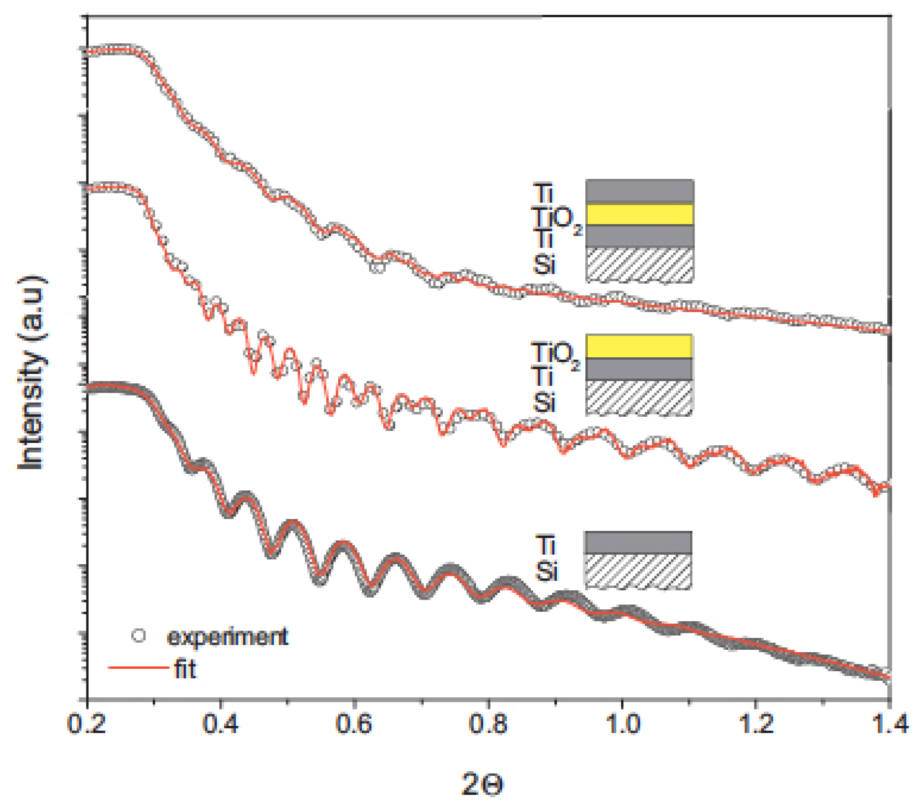
2)). To demonstrate the computational analysis process, a sample set of interference spectra is included in
Figure 5, which is a combined graph of three independent sample traces for titanium and titanium dioxide films deposited on silicon substrates in approximately 50 nm layers [
48]. The data are fit in each case with a parameterized equation that yielded the thickness, roughness and density for each film involved. However, it should be noted that as the number of layers increased, the number of necessary parameters also increased, and the resultant fit became less accurate. Additionally, the similarities in electron densities between layers of Ti and TiO
yield less distinct interference peaks than are generated by the differing densities at the Si–Ti layer on the bottom of the intensity plot.
Nevertheless, with regard to the thickness, the measurements based on the single film layer were most accurate, with a margin of error of only ±1 nm; whereas for the triple film layer sample, the margin of error increased to ±2 nm for each film thickness. The plot also demonstrates that as the overall film thickness increases, the interference intensity curve undulates to a lesser extent, which lessens the accuracy of the parameterized fitting functions. Consequently, the increase in error observed in the multi-layer films is directly resultant from their collective thickness.
Additionally, although the equipment measured the same film with subsequent depositions, the measurements for each of the films changed as additional films were deposited on top. This is to be expected, as the mean free path of the photon is insufficient to accurately measure films beyond approximately 100 nm. XRR relies on the penetration and subsequent reflection of X-ray photons at the interfaces between material boundaries; however, with increasing sample thickness, the incident photons stand a greater chance of absorption, scattering or diffuse reflection, all of which diminish the specular reflectance measurements and, thereby, decrease the accuracy of the parameterized fit [
49]. Nevertheless, the accuracy of the fit for ultra-thin films on the order of 25 nm is extremely good, with measurement error falling to around only ±.3 nm [
52]. As such, in the course of metal film characterization, if the film thickness is known to be less than 100 nm, XRR is likely to produce reliable measurements of film thickness; although, it will not yield information about the properties of the film in the visible spectrum.
2.2. Ellipsometry
Another optically-based characterization technique, ellipsometry, was initially established 100 years ago by Paul Drude in Germany; however, it was only with the advent of modern computing and phase modulation that the true strength of the technique as a characterization tool was demonstrated [
53]. As with spectrophotometry, ellipsometry uses visible light to derive thin film properties; however, the analysis is much more accurate, as it incorporates changes in both reflected amplitude and phase. As above, the subsections that follow introduce the operational theory behind ellipsometry, the methods for its use and the procedure for obtaining film thickness measurements from the resultant data.
2.2.1. Ellipsometry: Theory
Ellipsometry builds on many of the same principles that were established by spectrophotometry, but more acutely measures the changes that result following the reflection of the incident beam of photons off each interface. The technique utilizes linearly-polarized visible light, which may also be scanned through a spectrum of wavelengths, to illuminate a sample surface at a designated angle of incidence, θ. Under such situations, when the polarized light intersects the interface, as with the X-rays discussed earlier, a portion of the beam will reflect away from the interface, whereas the remaining portion will transmit down to the next interface. The strength of ellipsometry, however, is derived from the amplitude of the reflected beams along with the phase shift that occurs as the beam refracts and reflects within each layer.
Building on that foundation, the linearly-polarized light can be considered to be a product of separate transverse magnetic (TM or “p-polarized”) and transverse electric (TE or “s-polarized”) components. The Fresnel equations, shown in Equations (
4) and (
5), express the reflection coefficient for each of these conditions at the interface of two media:
wherein
and
are the coefficients for each of the the p- and s-polarizations, respectively,
and
are the complex refractive indices for the incident and secondary media and
and
are the angles of incidence and refraction.
Given that the thin films in question are deposited on a substrate layer or may incorporate multiple consecutive layers, the reflection coefficients for each subsequent layer must all be incorporated into the total reflection coefficient. The expressions for a simple three-layer system (e.g., air-film-substrate) are provided in Equations (
6) and (
7) below:
For these equations,
represents the reflection coefficient at the air-film interface, whereas
represents the reflection at the film-substrate interface. For more complex systems, additional components must be incorporated for each subsequent interface. Additionally,
β is incorporated as an expression of the phase change that occurs from the top to the bottom of each layer:
which is dependent on the wavelength
λ, refractive index of the refracting medium
, angle of refraction through the medium
and the film thickness
d [
54]. Consequently, by measuring the phase shift and reduction in amplitude of the reflected beams relative to the known and controlled light source, computational analysis may be performed to determine a value for
β and thereby derive the complex refractive index and film thickness of each layer.
2.2.2. Ellipsometry: Method
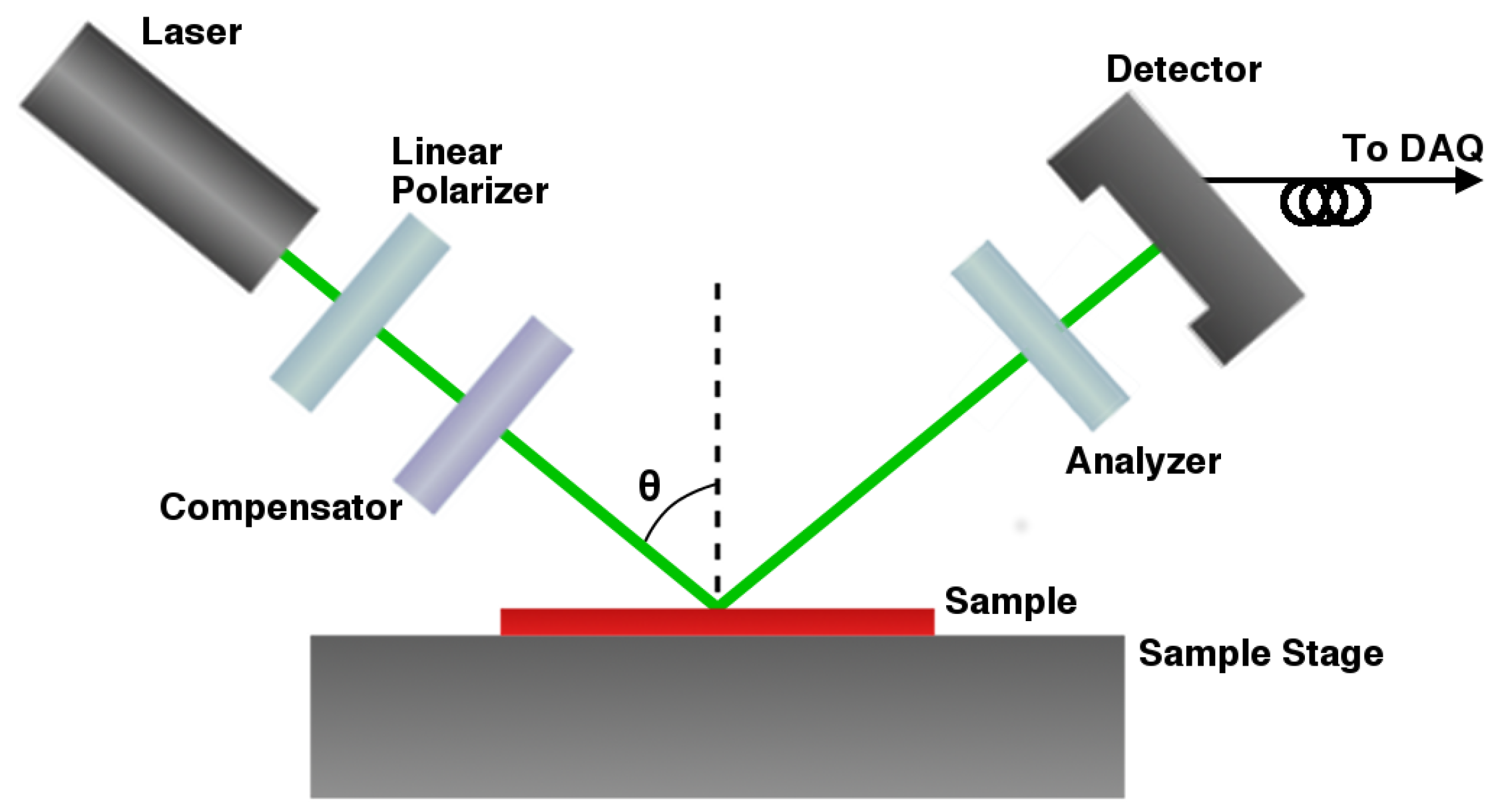
Modern ellipsometers typically contain a specific series of specialized optical components in order to accurately track the effects on a beam of light resultant from reflection off a multilayered surface.
Figure 6 depicts the components necessary for properly performing ellipsometric analysis on a thin film sample, which may be modified to include additional components as needed. However, regardless of the application, the system will typically proceed along the same progression of optical components. First, a collimated light source generates a beam of light, which is transmitted through a linear polarizer and subsequently passed through a compensator, which is typically either an electronic phase modulator or quarter-wave plate. The purpose of these components is to afford control over the incident polarization state of the light, so as to accurately measure the phase change upon reflection.
The final components incorporate an analyzer and a detector pair, which allow for independent measurement of the resultant wavelength-dependent phase shift and reduction in amplitude resultant from reflection. Additionally, the components are typically also mounted on a goniometer, which allows for the incident reflection angle to be modified between spectra. Based purely on the optical theories presented in the previous section, it is possible to derive the film thickness using either a single wavelength throughout a spectrum of angles or, alternatively, a spectrum of wavelengths operating at a single reflection angle; however, due to the strong dependence of refractive index and optical absorption on wavelength, in addition to the effects of chromatic dispersion, it is often advisable to perform multiple wavelength spectra at various angles of incidence to reduce measurement errors.
Most modern ellipsometers utilize software that is designed to fit a parameterized model to a spectrum of wavelengths as opposed to a spectrum of angles; although, if possible, it may also be beneficial to record measurements at a variety of incident angles and to average the derived values for each fit, as recording both wavelength and angular spectra can help to mitigate sources of error in parametric fitting. The spectra typically range from the upper end of the UV to the lower end of the near-infrared regions. For applications involving metal films, it should be noted that UV light tends to be largely absorbed by most metals, and as such, shorter wavelengths are not ideal for producing reliable data. Additionally, infrared wavelengths tend to be absorbed by adsorbed water molecules or other organic molecules in the local atmosphere, which may add measurement error to the resultant film thickness calculations; although, applications for infrared wavelengths in characterizing certain metamaterials and organic films have been demonstrated [
55].
2.2.3. Ellipsometry: Analysis
After recording the reflected intensity and the phase change for both s- and p-polarizations for each wavelength in the spectrum, the ellipsometry software will create a complex reflectance ratio of the reflectivity for p-polarized light,
, divided by that of the s-polarized light,
, given by Equations (
6) and (
7), respectively. This ratio can also be expressed as:
where tan(Ψ) represents the amplitude reflectance ratio of the two polarizations and Δ represents the phase change [
56]. As was the case with spectrophotometry, since the optical properties are wavelength dependent and are derived alongside the film thickness, ellipsometry uses a spectrum of incident wavelengths in order to determine these values. The principal difference between the two is that by observing the change in phase in addition to the change in amplitude, the parameterized model takes a two-tiered approach dependent on two independent variables and, consequently, produces more accurate results.
At this point, there are various methods of determining thickness from the ellipsometry measurements. One of the original methods involves substituting Equations (
6) and (
7) into (
9) [
57]. The resulting equation can be rearranged to yield a quadratic equation of the form:
Solutions to Equation (
10) yield two values for the film thickness; however, measurement conditions may cause both solutions to be complex, so with this method, the real component of the solution with the smallest imaginary component is used. Alternatively, more accurate methods of retrieving the thickness and refractive index values from the relationship in Equation (
9) have been developed to computationally fit the data to an appropriate model, as shown in
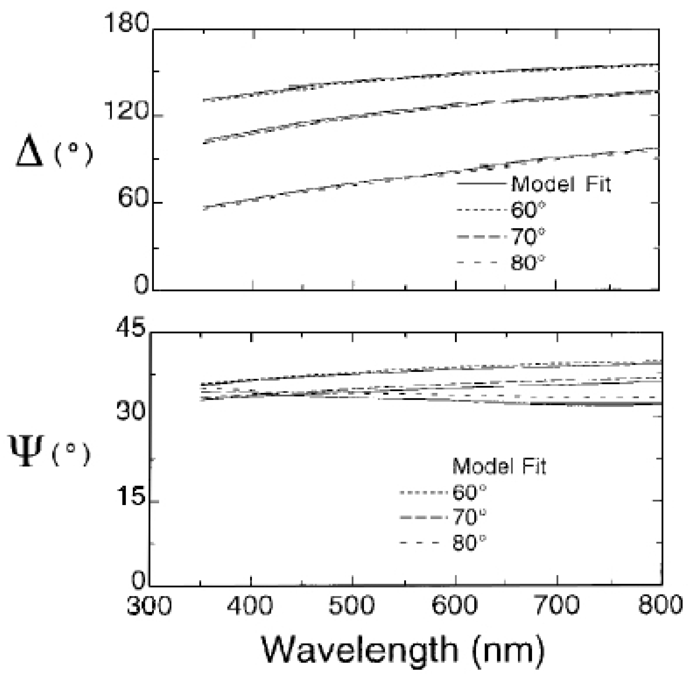
Figure 7 [
58]. Often, the model selection comes down to the preference of the user, although it is typically advisable to take the “simpler, better” approach, unless there is reason to involve additional variables [
59]. It is important to note that this model will not be an exact fit to the data, particularly for multilayered, thicker or more optically-absorptive metal thin films.
For example, since optical absorption is wavelength dependent, the deviation from theoretically predicted values will also change based on the incident wavelength. Although the theoretical equations do incorporate the complex component of the refractive index into the calculations, it is challenging to separate amplitude loss due to absorption from that due to transmission or scattering. Additionally, the optical penetration depth of a photon into a material is a function of wavelength, which would suggest that longer wavelengths will penetrate more deeply into the material, which may alter the accuracy with which a film’s thickness is measured. Consequently, there will likely be a significant degree of error in the thickness and refractive index values output by the software for metal and other optically-absorptive thin films. Additionally, this error compounds with increasing film thickness, so much so that many ellipsometer manufacturers advise against utilizing ellipsometry for films thicker than 50 nm, as the values may no longer be considered reliable.
2.3. Profilometry
The field of profilometry encompasses a wide variety of techniques utilized for surface topographical analysis with sub-nanometer resolution. Although Scanning Probe Microscopy (SPM) and Scanning Tunneling Microscopy (STM) may be used in certain cases for the analysis of thin film thickness, they necessitate that the sample be electrically conductive; and whereas the metal films in question are indeed conductive, it is common for them to be deposited on insulating glass or ceramic substrates [
60]. As such, Atomic Force Microscopy (AFM) is typically utilized instead, since it measures mechanical tip deflection rather than electrical current and, consequently, is not subject to such electrical limitations [
61]. Stylus profilometers may also be utilized; however, AFM systems tend to have superior resolutions due to tip size and shape.
2.3.1. AFM: Theory
Unlike other surface analysis methods, AFM measures the surface profile and film thickness through direct correlation with a mechanical action, as opposed to calculating derived values by data-fitting a theoretical model. Whereas the previously discussed techniques have each been based on various forms of radiative reflection, this technique functions by directly measuring the deflection and corresponding oscillation of a flexible, microscopic cantilever tip caused by attractive and repulsive atomic forces experienced as the tip is moved vertically with respect to the film’s surface. At relatively long distances, the attractive van der Waals forces will dominate the action of the tip, resulting in a characteristic deflection toward the surface relative to the strength of the force, as can be seen in
Figure 8 when the approaching tip makes contact. Following contact, however, the repulsive Coulombic forces will begin to dominate, causing an opposing deflection, which is measured in the increasing Z voltage. As the tip is retracted away from the surface, the attractive forces begin to dominate again and hold on to the tip, resulting in an inversely concave deflection until reaching a threshold at which the forces are no longer sufficient to hold the tip and the voltage returns to baseline. Moreover, by moving the tip within the transition region between attractive and repulsive forces, the these forces can generate a spring-like oscillation in the cantilever, whose frequency is characteristic of the surface being analyzed.
In order to achieve high resolution, the cantilever tip must be manufactured to be only a few nanometers thick at its tip. However, because the oscillations are resultant from atomic forces, AFM does not necessitate that the sample be either conductive, as is the case with scanning probe microscopy and scanning tunneling microscopy, or optically reflective or transparent, as is the case with light-based methods. Additionally, since the tip effectively measures the strength of atomic forces, AFM is capable of characterizing surface properties in addition to surface geometry. Moreover, AFM may be utilized to generate a three-dimensional surface profile by raster scanning the surface with the cantilever and recording the deflection with respect to the horizontal grid system. In this manner, a 3D reconstruction of surface geometries may be computationally reconstructed; however, in order to specifically measure the thickness of a thin film, it is necessary to raster the tip across a transition region, wherein the discrepancy in the vertical position of the film’s surface and the substrate layer may be measured, such as a border or furrow. The waveguides discussed in
Section 1.1 are fabricated with masked-off active areas, which when removed expose the underlying substrate material and provide a significant transitionary region between the substrate and metal-film clad sections.
However, in cases wherein the film is homogeneously deposited across the substrate surface, another method for measuring the thickness with AFM is to scratch the film and measure the depth of the scratch [
62]. For sufficiently thin films, the scratch will penetrate down to the substrate and result in an accurate thickness measurement; however, care should be taken with this approach, as an insufficiently deep scratch will not yield a measurement of film thickness, but instead simply a measure of the depth of the scratch in the film. Moreover, if no transition occurs by design, the scratch method necessitates damaging the surface of the sample and is no longer a completely non-destructive technique. Additionally, if the cantilever tip is used to generate the furrow in the film, it must also be resilient enough to subsequently scan the film; AFM tips sputter coated with titanium nitride have been demonstrated to be effective at such a task [
63].
2.3.2. AFM: Method
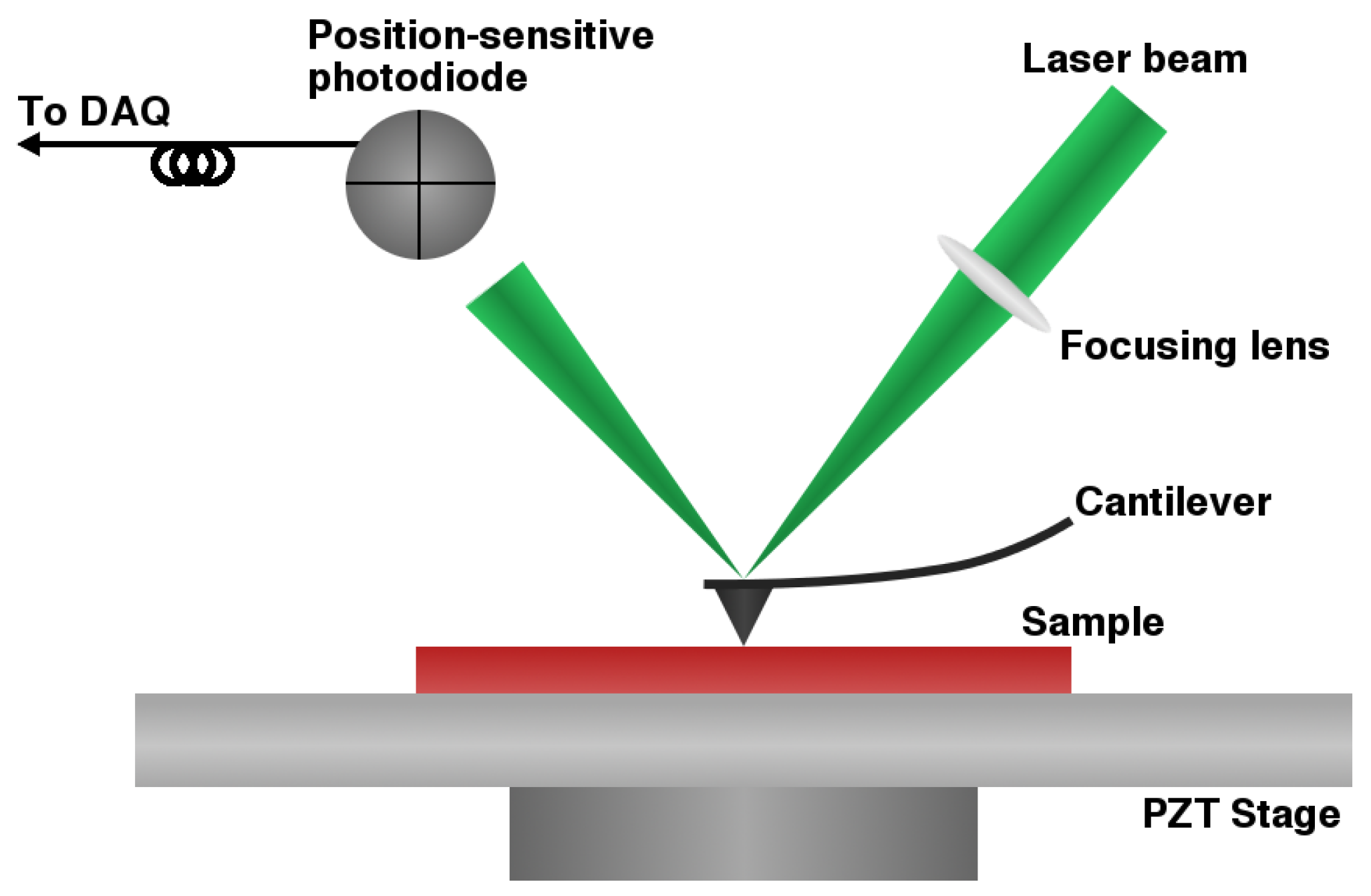
The method of operation for an AFM follows directly from the theory, requiring few components beyond the cantilever, tip and scanner. In addition, typical AFM systems incorporate a laser source, which focuses a beam of light onto the rear face of the cantilever tip, and a photodetector, which analyzes the intensity of the beam reflected off the tip, as shown in
Figure 9. The apparatus may also include a voltmeter or an arbitrary waveform generator in order to either measure the oscillation of the cantilever or drive the oscillation with an applied waveform.
The AFM system may be operated in contact mode, wherein the tip remains in contact with the sample surface throughout testing, or tapping mode, wherein the spring-like undulation of the cantilever tip is used to measure surface properties based on attractive and repulsive forces. Furthermore, the apparatus may be designed such that the Piezoelectric Translational stage (PZT) moves the sample stage with respect to a fixed cantilever setup or such that the cantilever and laser setup is moved with respect to a fixed sample stage; however, both orientations may produce comparable results. It should be noted that hysteresis in the piezoelectrics may lead to measurement artifacts and non-linear, inconsistent lateral resolution. However, for the purposes of film thickness characterization, as long as there is sufficient resolution at the transition between film and substrate, the thickness should be accurately measured. Additionally, if the cantilever tip is in motion across the surface, it is recommended to operate in contact mode to avoid the addition of any vibrations from the scanning action [
46].
2.3.3. AFM: Analysis
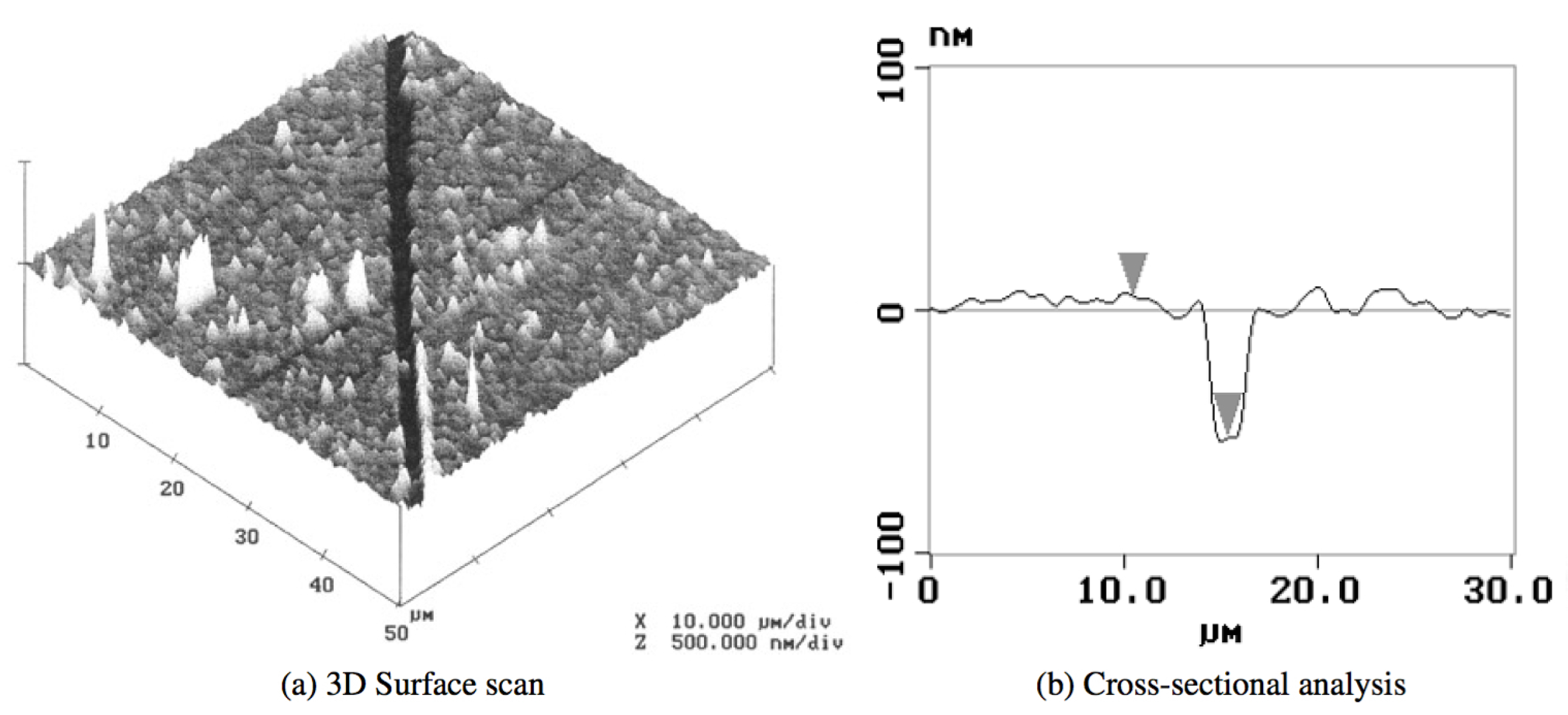
AFM analysis is much more straightforward than other techniques mentioned herein, since the reflected laser intensity directly corresponds to the position of the tip relative to the surface, assuming the system has been properly calibrated. Although only a single pass over the transition between film and substrate is necessary to measure depth, typically a full two-dimensional scan will be performed in order to generate a three-dimensional surface profile, such as that shown in
Figure 10. Scanning over a large area also ensures that variations, artifacts and debris on the film surface do not distort thickness measurements.
Film analysis in such a manner will not only reveal the thickness of the film, but also aspects of the transition area, like steepness and film homogeneity. For example, the study that recorded the AFM image shown in
Figure 10 also noted that in the course of scratching the furrow in the polymer film, the cantilever tip created ridges along one edge where the polymer had been pushed to one side. In order to compensate and accurately determine the thickness of the film, they scanned over a relatively large area (2500
), so that the baseline used as a top surface reference would not be distorted by the ridge height.
By scanning the cantilever tip across the furrow, the researchers were able to generate the cross-sectional profile shown in
Figure 10, which determined the thickness of the 14-bilayer film to be approximately 54 nm. Although the specific value is not quoted in the text, a graph of the number of bilayers plotted against the film thickness recorded by AFM was presented in the text, which demonstrated a linear relationship between the two. That said, typical AFM systems have a sub-nanometer vertical resolution, so as long as the transition between the substrate and the film surface is being observed, the thickness should be readily determined with a relatively low degree of error. It should also be noted that such measurements using a furrow to measure thickness will be fundamentally limited by the sharpness of the cantilever tip. Moreover, although AFM can indirectly measure the thickness of a thin film on a substrate without the need for complex curve-fitting, the technique provides little other information beyond thickness and homogeneity. Consequently, in relating optical transmission to metal film thickness, AFM is only capable of completing half of the analysis and, so, must be used in conjunction with an optically-based technique in order to complete the analysis.
2.4. Electron Beam Techniques
Electron beam-based technologies represent a categorically different alternative to traditional techniques that rely on electromagnetic radiation to interrogate sample surfaces. Although there are a number of different techniques that have spawned from e-beam approaches, including Auger Electron Spectroscopy (AES) and Transmission Electron Microscopy (TEM), two technologies have demonstrated particular application in determining thin film thickness: cross-sectional Scanning Electron Microscopy (SEM) and Energy Dispersive X-ray Spectroscopy (EDS or EDX). The former technique uses secondary generated electrons to computationally produce a two-dimensional image of a film cross-section, which may provide a clear depiction of the film sitting atop the underlying substrate layer. By contrast, the latter technique uses X-rays generated by the incident e-beam to characterize the elemental composition of the film, which may be compared to the elemental composition of the substrate to computationally determine the film thickness.
2.4.1. E-Beam Techniques: Theory
Both of the techniques mentioned may be performed using an SEM system, although the SEM-EDS necessitates a suitable X-ray detector in addition to the standard secondary electron detector used in SEM image generation. In both cross-sectional SEM and SEM/EDS analysis, a beam of electrons is directed in a column incident upon the sample surface, generating a variety of effects that are strongly correlated with the energy of the e-beam, each of which provide an array of information about the sample and can be utilized to determine a variety of its characteristics. For example, backscattered electrons may be used to determine sample crystallography; whereas Auger electrons may be detected to provide information about the surface composition.
Figure 11 depicts the characteristically bulbous electron beam interaction volume and demonstrates the various depths at which each effect is generated.
However, cross-sectional SEM analysis is principally concerned with the topography of the film cross-section and, so, utilizes the detection of secondary electrons generated within the sample through inelastic scattering. Although these electrons bear no significant dependence on the composition of the region of their origin, they are highly sensitive to topographical features [
64]. Consequently, these electrons are used to generate the traditional tomographical SEM images, which have become so prevalent in scientific literature and are widely used in observing and characterizing thin film surface homogeneity [
65]. The lateral resolution of such images is largely dependent on the incident beam diameter and the e-beam interaction volume, yielding surface tomographical images with resolutions well beyond the optical diffraction limit [
66]. The typical resolution of standard SEM is included in
Table 2, along with the resolutions, limitations and sample requirements of other standard material characterization methods.
Additionally, although the properties of the electrons themselves are not related to sample composition, the likelihood of their generation is dependent on the composition of the sample from which they originate, which produces a degree of contrast between surfaces of differing composition, such as a metal film and its glass substrate. Moreover, by increasing the tilt angle of the sample, it is possible to increase secondary electron generation and thereby increase the contrast. Images produced that demonstrate a discernible difference between the two surfaces are then analyzed to produce an estimation of the film thickness.
SEM-EDS, on the other hand, relies on X-rays produced through the interaction of the incident electron beam upon the sample surface [
67]. The high energy electrons bombard the sample and eject secondary electrons from the atomic orbitals. The ejection of said electrons leaves vacancies in the electron shell, which are filled by electrons in higher shells. When an electron drops down to fill the vacancy, an X-ray is produced, whose energy and wavelength are characteristic of the orbital from which it was generated and, therefore, are characteristic of the atom, as well. However, not all X-rays produced through this method are characteristic of the elements by which they are generated. The incident electrons can interact with any electrons in the atomic orbitals, which can generate a spectrum of other X-rays of differing energies [
37]. Nevertheless, the characteristic X-rays may be used to perform chemical analysis of the sample surface, which may be compared to the chemical composition of the substrate to determine the relative amount of each element in the film. Although not an absolute measure of elemental concentration, ratios of the relative amounts of the elements of interest may be generated to infer film characteristics or to compare the sample to other similar samples for differentiation purposes [
68,
69].
2.4.2. E-Beam Techniques: Method
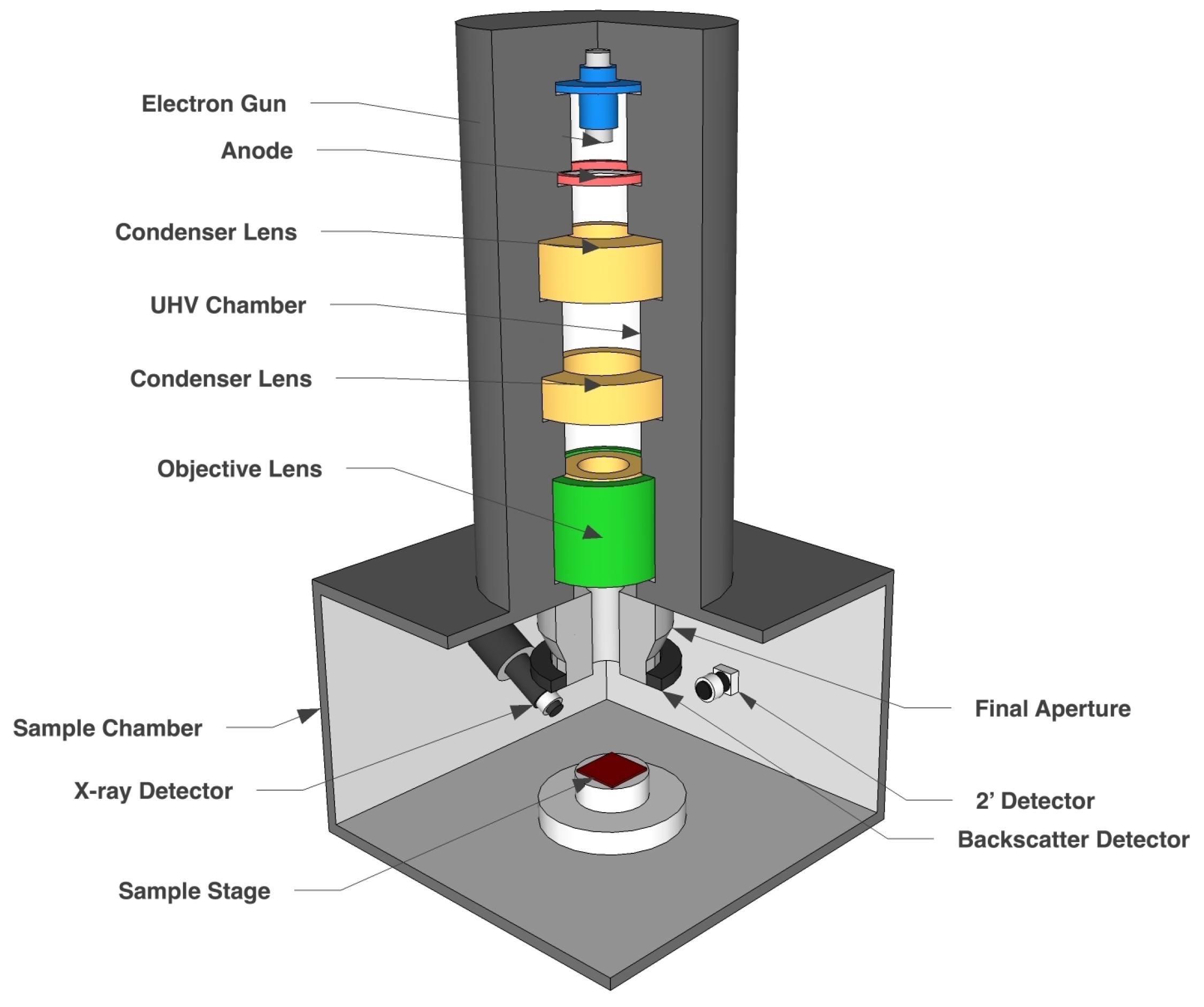
The electron beam may be generated through one of two different means: field emission or thermionic emission. In the former method, electrons are generated by placing a pointed cold cathode filament in a high potential electric field, which rips electrons away from the filament and directs them toward the sample. In the latter method, a strong current is passed through a conducting filament, which generates a beam of electrons that are directed toward the sample surface. Regardless of the method of generation, the electron beam must be created under a high vacuum in order to collimate the beam and prevent premature electron scattering. Consequently, the method of generation is considered a design parameter for the equipment, rather than an analytical variable in experimentation.
The beam is directed toward the sample through a column of electromagnetic “lenses”, which collimate, condense and focus the beam on the sample surface, as shown in
Figure 12. In addition to these lenses, a pair of scanning coils deflects the beam so that it may be raster scanned across the surface, so as to generate a two-dimensional image or to analyze a specific section of the sample. The SEM equipment may also incorporate detectors for each of the aforementioned phenomena; however, cross-sectional SEM generally utilizes only the secondary electron detector, whereas SEM-EDS uses both that and the X-ray detector for elemental analysis. In order to avoid artifacts caused by sample charging, operating the SEM at lower beam energies around 1.5 kV or less can yield operating resolutions around 1 nm, although insulating samples like the glass or ceramic substrates used in optics should still be properly grounded [
70].
Cross-sectional SEM analysis is functionally identical to traditional SEM in that a beam of electrons is directed toward the surface of a sample thin film-coated material. The principal difference is that the cross-sectional analysis necessitates that the region of interest be either the boarder of a thin film where the full thickness of the film atop the substrate can be observed or else is a surface created by cutting the sample to produce such a cross-section. In the event that an observable border is present by design, the procedure is non-destructive in nature; however, should there be no such facet, this technique may necessitate damaging the sample.
By contrast, SEM-EDS focuses the incident e-beam onto a sample spot that is analyzed for a set amount of time, typically around 100 , so that the electrons can interact with each element of the sample and under interrogation. Although EDS can be achieved using any e-beam system, the combination of EDS with SEM allows for the secondary electron imaging to be utilized as a targeting system. The SEM generates a two-dimensional image of an area of the sample, from which a point or series of points is selected for interrogation. Analysis of more points allows for statistical verification of film thickness, given that inhomogeneities may result in slight variations in thickness calculations.
2.4.3. E-Beam Techniques: Cross-Sectional SEM Analysis
With regard to thin film thickness measurement, cross-sectional SEM analysis is performed using image processing software, provided that an appropriate cross-section of the film and substrate layers has been recorded such that each layer is distinguishable from the others. Certain manufacturers include image processing as a tool incorporated into the equipment’s operational software; however, there are also a number of third party applications that perform the same tasks, including ImageJ, Gimp and Adobe Photoshop, assuming that a relevant scale has been included in the image. By comparing the height of the thin film in pixels over the length of the image to the scale provided by the SEM software, it is possible to calculate the thickness of the film in nanometers. The software may also need to take into account the magnification and the tilt angle of the mount in order to obtain an accurate reading, which may compound error and result in detrimental effects on the resolution of the technique depending on the accuracy of the mounting angle measurement.
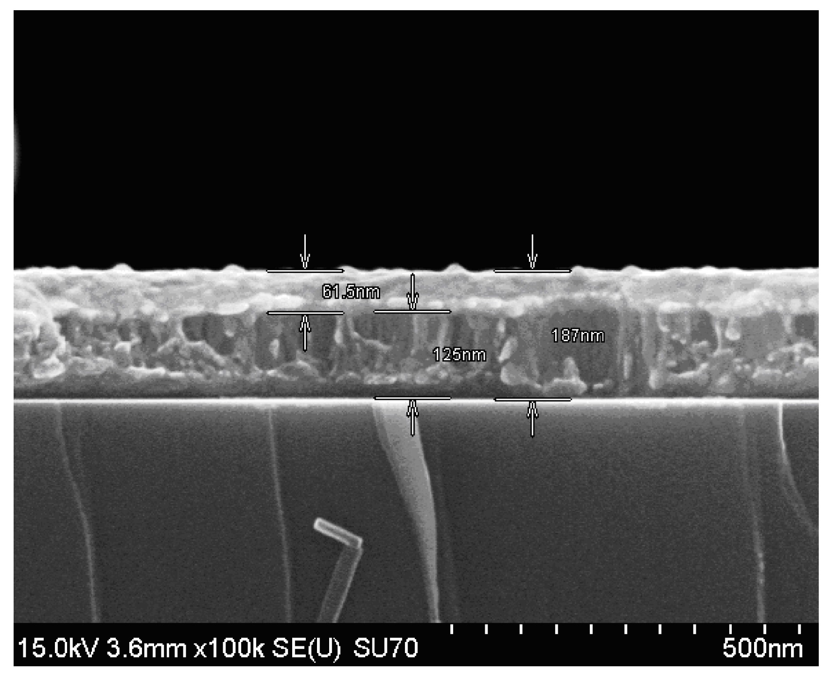
The SEM image shown in
Figure 13 demonstrates an example of a two-film system deposited on a silicon substrate [
34]. The system under interrogation consists of a thin gold film deposited over a nickel film adhered to the surface of the silicon substrate, each of which is clearly distinguishable due to the distinct difference in contrast presented by each material. The image was analyzed using the LayerProbe software and yielded thicknesses of 60.1 nm for the gold film and 123.5 nm for the nickel film. The paper also reported that measurements had been recorded for the same system using X-Ray Fluorescence (XRF), yielding thickness values of 61 nm and 141 nm, respectively. Moreover, the software claims that the resolution for each measurement is 0.7 nm for this analysis, although in other cases, the error was as low as 0.1 nm; whereas the resolution of XRF measurements was only 25 nm and 24 nm, respectively [
34].
These values suggest that SEM image analysis can provide an extremely accurate measurement of film thickness; however, the situation presented is an ideal example wherein the films are easily distinguished and there does not appear to be any blatant image aberration. Under less-than-ideal situations, the measurement resolution is quickly compromised due to confounding factors, such as image aberrations, distortion, lack of contrast and charge build-up. Moreover, the facet chosen for analysis may not be representative of the entire surface, so obtaining an accurate thickness measurement may necessitate the destruction of the sample such that additional cross-sections may be imaged. Whereas other methods of analysis may non-destructively analyze different portions of the film, whether through raster-scanning the sample surface or independently changing the investigated area, cross-sectional SEM reveals only information about the observable face. In cases where the sample is inhomogeneously deposited, cross-sectional SEM may yield inaccurate or misleading measurement. Consequently, SEM analysis is often used to visually present the film geometry and thereby gain an estimation of its thickness and surface roughness, but is typically used in conjunction with another analytical method for a more accurate empirical measure.
2.4.4. E-Beam Techniques: SEM-EDS Analysis
In performing SEM-EDS analysis of a sample thin film deposited on a given substrate, the SEM imaging system is utilized as a targeting system so that the regions of interest can be identified by the user and interrogated by the e-beam. Each element yields characteristic X-rays resultant from electron interactions with electrons in the core atomic orbitals, allowing for the recording of an X-ray energy spectrum, which depicts the relative presence of each element based on the amplitude of recorded X-rays by their characteristic energy. In order to accurately record ultra-thin films of elements with high characteristic X-ray energies, a high speed silicon drift detector is necessary, due to the need to process counts at a sufficient rate to record the shorter wavelength X-rays.
Chininis et al. utilized an SEM equipped with a Bruker Quantax 200 Silicon Drift Detector with Xflash6 to interrogate samples of titanium and silver deposited on silicon glass substrates in order to determine the respective deposition rates of the two metals in a cold sputter vacuum deposition system [
9]. The X-ray energy spectrum recorded for each sample was utilized to compare the peak amplitude of the silicon peak to that of the element being analyzed, as shown in
Figure 14. Silicon was used due to its stability within the glass chemistry, allowing for the recording of reliable counts per second by electron-volt (cps/eV) for each of the relevant elements in the sample.
Following that, elemental ratios of silicon to the element of interest (either silver or titanium) were generated, and the NIST DTSA-II (National Institute of Standards and Technology Desktop Spectrum Analyzer-II) software was used to produce a simulation of experimental conditions, while iteratively varying film thickness on a homogenous substrate in order to compare the recorded elemental ratios to those predicted though simulations. The ratios of silicon/titanium and silicon/silver were calculated for each simulation, varying film thickness until the ratios matched the recorded data, allowing for the determination of film thickness by comparing recorded measurements to the theoretically predicted models. The authors were able to calculate thickness measurements in such a manner and to determine the titanium deposition rate to be 0.10 and the silver deposition rate to be 1.19 . Consequently, provided the SEM is equipped with an appropriate X-ray detector, it may be possible to perform calculations to determine the film thickness by comparing measured values to DSTA software simulations based on NIST data.
3. Limitations and Considerations in Thin Film Characterization
The techniques discussed herein are some of the more useful methods of characterizing metal thin films. However, there are myriad other modalities for characterizing thin films, many of which are listed in
Table 2. Each of these technologies has its benefits, but many are poorly suited to characterizing metal thin films in particular. Some of the more common limitations are included in the sections to follow, along with some useful considerations for the interested reader.
3.1. Radiative Absorption
Many of the techniques mentioned herein and included in
Table 2 are based on some form of photon propagation, whether within the X-ray, UV, visible or infrared spectra. Consequently, these methods are subject to the influence of the optical properties of the samples in question, such as their absorption and scattering coefficients. This work focuses on metal films, where samples are largely reflective, particularly at greater thicknesses; however, they also tend to have a non-zero absorption coefficient, which is incorporated as part of the complex refractive index
, where
n is the real portion of the refractive index, which governs the relative speed of light in the medium, and
κ is the imaginary component, which governs optical absorption.
The complex refractive index, and therefore, the absorption of photons, may have a profoundly negative effect on the efficacy of any radiative technique, particularly techniques like XRR and ellipsometry, which rely heavily on specific changes resultant from the incident beam partially reflecting off the front and rear faces of the sample at each film interface. The greater the absorption within the film, the less accurate the measured change will be. This is particularly true for thicker films, wherein significant absorption reduces the effective mean free path of the photons passing through the film, which consequently decreases the number of photons that are able to escape the medium and therefore the intensity of the detected beam. This effect may alter the amplitude of the reflected intensity profile and skew the data away from the true values of film thickness, which can have a compounding effect for techniques that rely on computational curve fitting for thin film analysis. It is for this reason that many thin film characterization companies state that their software is only reliable for metal films between 0.5 and 50 nm thick, beyond which regimes, the software can no longer accurately match the model to the data in a reliable fashion; although custom-built laboratory equipment may be able to out-perform commercially available equipment.
Figure 5 is a principal example of such limitations, as the data for the thicker films are less defined and resulted in a poorer parameterized fit. The margin of error in the fit resulted in a slightly worsened resolution, as well. It is advisable, therefore, that the radiative absorption spectrum of the elements that comprise the sample be considered when selecting a radiative technique, given that metals may be highly absorbing in the one spectral regime, but largely transmissive in another.
3.2. Sample Conductivity
Another significant category of techniques utilized in thin film characterization involves the use of electron beams, as are used in SEM and Auger Electron Spectroscopy (AES), beams of charged ions, as used in Medium Energy Ion Scattering (MEIS), or electrical current, as employed in Scanning Tunneling Microscopy (STM). As a result, all such techniques are subject to the likelihood of charge build-up on the sample surface if not appropriately grounded, which can have substantial consequences for both the resolution of the technique and the serviceability of the equipment.
This work focuses on metal films in optical applications, which frequently involve film deposition onto optically-transparent, but electrically-insulating substrates. That being the case, electrical charge build-up is a strong possibility. Techniques like SEM, which rely on the detection of electrons ejected from the sample, utilize incredibly sensitive equipment designed to detect small amounts of electrons. Consequently, a charge build-up may permanently damage the detector/analyzer, but will almost certainly “white-wash” the SEM image, thereby disrupting the necessary contrast for discerning film layers, deteriorating the spatial resolution of the image and rendering any desired tomographical profile unreliable. Operating at a lower vacuum and reintroducing gases into the SEM may improve contrast and allow for charge to be conducted away from the sample surface, but also introduces a greater likelihood for e-beam interaction with the gas in the form of diffraction or scattering, which can have a negative influence on spatial resolution.
Moreover, techniques that employ X-ray radiation may also suffer from charge-related problems as X-rays of such a wavelength are capable of interacting with the valence electrons in metal films and thereby elevating them to a higher energy state or otherwise ejecting them away from the film surface entirely. In the case of XRR, the charge build-up may damage the equipment as it discharges to other components, but may also affect the intensity of the specularly-reflected beam. The use of conductive adhesive, such as copper tape, to form an electrical connection between the film layer and the sample stage may mitigate charge build-up concerns, but may have undesirable consequences on the adhesion regions of the sample, undermining otherwise non-destructive techniques.
3.3. Derived vs. Measured Thickness
Although
Table 2 lists a number of other limitations and considerations, perhaps the most important consideration to bear in mind is the difference between computationally-derived film thickness values, such as are provided by techniques like UV-VIS Spectrophotometry, XRR and ellipsometry, and thickness values directly correlated to an empirical measurement, as are provided by techniques like STM and AFM. The latter variety are typically contact-based technologies that often offer sub-nanometer depth resolutions and extremely reliable measurements owing to the use of vibration-damping systems to mitigate noise and error; however, they also necessitate transition regions on the samples to provide vertical contrast between substrate and film layers and, as such, are limited either to only those samples that incorporate such regions or those samples that allow for destructive testing conditions.
When such conditions are not met, the former variety of techniques is preferable, typically guaranteeing non-destructive testing and nano-scale resolutions. However, such methods rely on computational modeling or curve fitting to derive film characteristics and, as such, are only as accurate as the margin of error for the models. Consequently, the parameters of the model, such as refractive index and film thickness, may place limitations on the reliability of the measurement, as the error residuals increase.
Figure 5 again provides an example wherein the analysis of thicker films exhibited greater error in the model fit and a correspondingly worsened depth resolution. As a result, derived thickness values are subject to computational error, inaccuracies of fit and potentially substantial deviations away from the theoretically-expected model. Moreover, when making use of any such computational techniques, it is essential that the operator also be aware of the theoretical assumptions upon which the software is operating. Moreover, said assumptions will likely change based on the various types of models and statistical analyses available in the software.
4. Conclusions and Developing Technologies
Due to their reflectivity and optical absorption, metal thin films often provide a challenge for many of the most predominant characterization techniques available. Of the methods covered in this review, AFM provides the most accurate and reliable measure of film thickness, with a potentially sub-Angstrom resolution, although it provides little other information and places certain requirements on the samples. Following that, SEM/EDS offers both an image of the film surface, which may grant information about the surface homogeneity, along with a computationally-derived film thickness and elemental composition spectrum. The resolution is not quite on par with AFM, but for the purposes of film analysis in optics and biophotonics, it is sufficient, given that the technique can analyze films regardless of their optical reflectivity or absorption while still offering an optically-relevant thickness measurement.
On the other hand, the other techniques, both based on radiative measurements, demonstrate varying efficacy and are highly dependent on the film thickness, absorption and refractive index. Ellipsometry is reportedly limited to metal films less than 50 nm thick, whereas XRR can reliably double that limit, although the degree of error in thickness value grows as thickness increases. In contrast to the other techniques, cross-sectional SEM does not actually provide a thickness value. However, image analysis can afford the observer with an idea of the overall thickness and the homogeneity of the film over a broad surface area. That said, it only provides local thickness characteristics at the cross-section and, therefore, would necessitate that the sample be fractured into multiple pieces to generate more cross-sections to analyze for statistical reliability.
Consequently, it is the opinion of the authors that if the refractive index of the metal film is of little to no consequence, contact-based profilometry techniques like AFM offer the most reliable measurement of thickness alone. In the event that a transition region is not incorporated nor destructive testing methods permissible, SEM/EDS is a suitable alternative technique, if available. Alternatively, each of the other techniques, particularly XRR, can provide reasonably accurate estimations through their derivations; however, investigators should be aware of the operational limitations of the techniques. It is recommended that should AFM or SEM/EDS not be a viable option, a reliable measure of thickness may be obtained through the combination of a radiative technique with cross-sectional SEM. Moreover, should the optical properties of the film be unknown and desired, employing additional thickness characterization techniques as confirmation can add reliability to radiative methods whose derivations may depend on geometric and optical parameters.
Having introduced some of the more predominant characterization methods and included a table of potentially viable alternatives that have seen some use in the literature, it is worth noting that there are also new techniques in development for the characterization of thin films. One such technique, Total Internal Reflection Photoacoustic Spectroscopy (TIRPAS), falls into the category of Evanescent Field-based Photoacoustics (EFPA) and has been demonstrated in the characterization of the thickness and refractive index of optically-transparent thin films [
71]. Variations of the same technology have been suggested for use with metal and other optically-absorptive thin films, in the form of Surface Plasmon Resonance Photoacoustic Spectroscopy (SPRPAS) and Optical Tunneling Photoacoustic Spectroscopy (OTPAS), in addition to applications involving the detection of absorbing particles [
38,
72].
EFPA techniques utilize the same evanescent field depicted in
Figure 2, but with the intention of generating acoustic pulses following the absorption of the field’s optical energy. In such applications, a sufficiently short laser pulse (less than 1
) totally internally reflects within a prism or waveguide, thereby generating an evanescent field within the external medium, which is typically the sample thin film. The portion of the field that penetrates through the film may be absorbed by chromophores in the medium beyond the film, which in turn incites an ultrasonic pressure wave through the optical absorption and resultant rapid thermoelastic expansion of the absorber. This acoustic energy may then be detected by a suitable ultrasonic transducer, which yields information about the film’s optical and geometric properties, including refractive index and thickness [
73]. The peak-to-peak magnitude of the photoacoustic pressure wave is directly related to the film thickness, its refractive index and the incident angle of the laser beam. Consequently, by scanning through a range of incident angles, it is possible to determine the critical angle of the film-prism interface, calculate the refractive index using Snell’s law based on the known refractive index of the prism and thereafter derive the film’s thickness. Although this method has similar limitations to the other aforementioned optical approaches, the range of detectable film thicknesses is theoretically directly related to the wavelength of the incident light. Consequently, for thicker films, a longer wavelength should ideally provide accurate results, whereas for thinner films, a shorter wavelength may prove more effective.
Considering the recent breakthroughs in thin film chemistry, film deposition techniques and meta-material fabrication, along with the continuous stream of new optical thin film applications being envisioned each year, the accurate depth profiling of thin films on insulating substrates represents a critical milestone in the advancement of optical technologies. This is particularly the case for technologies akin to the waveguides discussed in
Section 1.1, which rely on sub-wavelength electromagnetic effects, such as evanescent field interactions and surface plasmon resonance, to achieve what macroscale techniques could not. As such, whether considering a new conceptual modality still being substantiated or an established technique being iteratively improved, the further advancement of both noted and novel thin film characterization technologies is anticipated to play a significant role in the future of optics and photonics.


