Article

Deposition of High Conductivity Low Silver Content Materials by Screen Printing

College of Engineering, Swansea University, Swansea SA2 8PP, UK
*
Author to whom correspondence should be addressed.
Coatings 2015, 5(2), 172-185; https://doi.org/10.3390/coatings5020172
Submission received: 8 February 2015 / Revised: 24 April 2015 / Accepted: 29 April 2015 / Published: 12 May 2015
(This article belongs to the Special Issue Trends in Coatings and Surface Technology—Feature Papers)

Abstract

:
A comprehensive experimental investigation has been carried out into the role of film thickness variation and silver material formulation on printing capability in the screen printing process. A full factorial experiment was carried out where two formulations of silver materials were printed through a range of screens to a polyester substrate under a set of standard conditions. The materials represented a novel low silver content (45%–49%) polymer material and traditional high silver content (65%–69%) paste. The resultant prints were characterised topologically and electrically. The study shows that more cost effective use of the silver in the ink was obtained with the low silver polymer materials, but that the electrical performance was more strongly affected by the mesh being used (and hence film thickness). Thus, while optimum silver use could be obtained using materials with a lower silver content, this came with the consequence of reduced process robustness.

1. Introduction

In total the silver ink market is estimated to be worth around $760 Million in 2012 [1]. Silver inks fall into three main categories, silver solutions, micro particle inks (particle size > 1 μm) and nano particle inks (<1 μm). The nano particle inks are of increasing interest as they offer lower sintering temperatures (for improved conductivity, which are appropriate to polymer substrates [2]. Nano silver materials have seen widespread research and development in inkjet [2], gravure [3] and flexographic printing [4].
Although the use of nano silver inks in inkjet and other printing processes is rising, thick film screen printing remains the dominant application technology in the market [5]. The patterning method of choice for large particle silver inks is screen printing which offers an ability to accurately deposit thick films with a large rheological window with minimum pressure over a wide area at economical production rates.
During the material formulation process the balance between silver quantity, particle size (and structure) must be considered in order to provide the required conductivity while maintaining film integrity, adhesion, flexibility and process compatibility. This requires a balance of conductive element, binder and solvent. The increase in the cost of silver over recent years, has led to development formulations which permit a reduction in silver quantity, without sacrificing conductivity or printability. Although the use of silver as a conductive material is widely reported, few published studies have examined the interactions between macro material properties, mesh characteristics and printed feature quality (predominantly topology and conductivity).
Screen printing of large particle silver materials is now the process of choice for metalizing silicon Photovoltaic (PV) cells, flexible circuits including membrane switch manufacture, Radio Frequency Identification (RFID) aerials and is also commonly proposed as a means of manufacturing many products within the nascent printed electronics arena. The increase in the cost of silver over recent years has led to the silver being the dominant factor in the bill of materials of many products and a prime driver in developing formulations with a reduced silver quantity, without sacrificing conductivity or printability. Although the use of silver as a conductive material for device manufacture (PV, sensors and RFID) by screen printing is widely reported, few published studies have examined the interactions between macro material properties, mesh characteristics and printed feature quality, particularly for systems which are cured at low temperature (<130 °C).
For lower temperature cured materials which are screen printed, the literature available on material or process parameters is sparse. As directly applicable literature is limited, it is pertinent to review associated relevant areas which have examined models for screen printing, solder paste printing through stencils and material/screen printing parametric studies whose objectives are within the scope of the present study. Theoretical studies of the process have made little advancement in the development of reliable screen printing process models. Early models showed some predicted trends which were in agreement with experimental observation but even the most recent developments require significant oversimplification (e.g., material viscoelasticity is ignored) which limit practical use [6,7]. Establishing process/material characteristics and their impact on printed performance therefore is reliant on experimental studies.
The importance of material flow properties and its interaction with the image carrier has been identified as the primary factor in determining feature rendition in solder paste printing [8] (which utilises a non-woven stencil and high temperature sintering). Much of the literature relates to silver materials which are used for metallization in the silicon PV industry where materials are fired at high temperature. The role of silver particle size and particle packing on silicon PV performance has been addressed [9] but this did not directly measure the impact of size on the material flow properties or printed feature conductivity. The flow characteristics of silver materials have been carried out but the subsequent relationship with the printed line quality has not been studied [10].
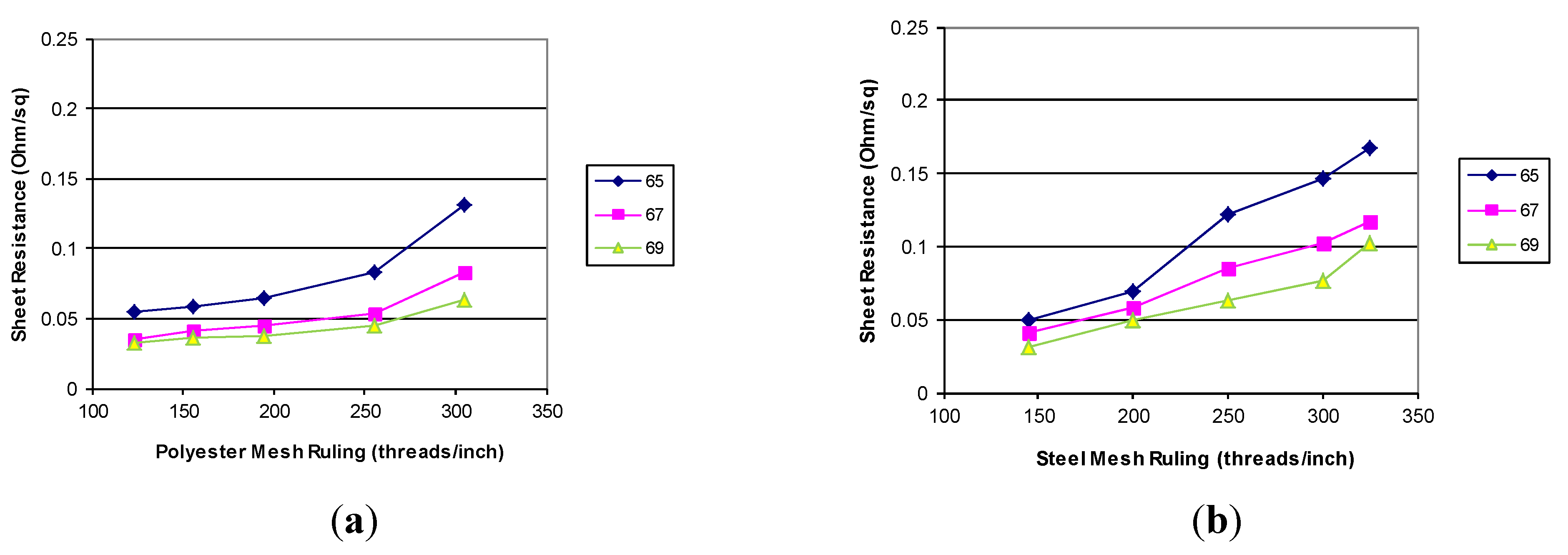
The role of the screen has been examined and this showed some general trends between the printed line quality and the mesh characteristics with line resistance reducing and line aspect ratio increasing as the screen open area proportion increased [11], although the scope of the study and analysis carried out was limited. The influence of squeegee pressure found some correlation between the applied pressure and the silver deposit characteristics [12] but this was limited to one mesh type and hence a limited film thickness. The net effect of formulation on the reliability of circuits has been examined [13] but this again was carried out at one mesh/film thickness. For carbon materials, the interactions between material properties mesh, structure and their impact on printed deposit topology showed non linear relationships between mesh ruling and sheet resistance, line resistance and film topology [14].
The review of the literature has demonstrated that there is a void in the understanding of the relationship between mesh type used, the properties of the silver materials (which are cured at low temperature) and the properties of the final printed film. At present, there is limited opportunity for developing models based on the exact physical mechanisms that take place during the printing process and linking this to material characteristics. In order to develop further understanding an investigation was therefore carried out which examined the role of mesh, physical silver ink characteristics on the topology and conductivity of fine lines. The investigation had three primary aims. Firstly, it aimed identify the role of silver content and binder properties on the microstructure of the cured films and their subsequent impact on electrical performance. Secondly, it aimed to establish the capabilities of lower silver content materials and their sensitivity to changes in film thickness. Finally, it aimed to create a reference dataset which could be used as a design tool which would identify material requirements and process settings given design specifications or likely print results given materials and process settings. These outputs would be significant benefit to the material formulator, device designer or process engineer.

2. Experimental Section

In order to investigate the relationship between formulation and film thickness a full factorial experimental design was employed where six silver materials were printed through 10 screens. The silver materials represent two formulation types, 
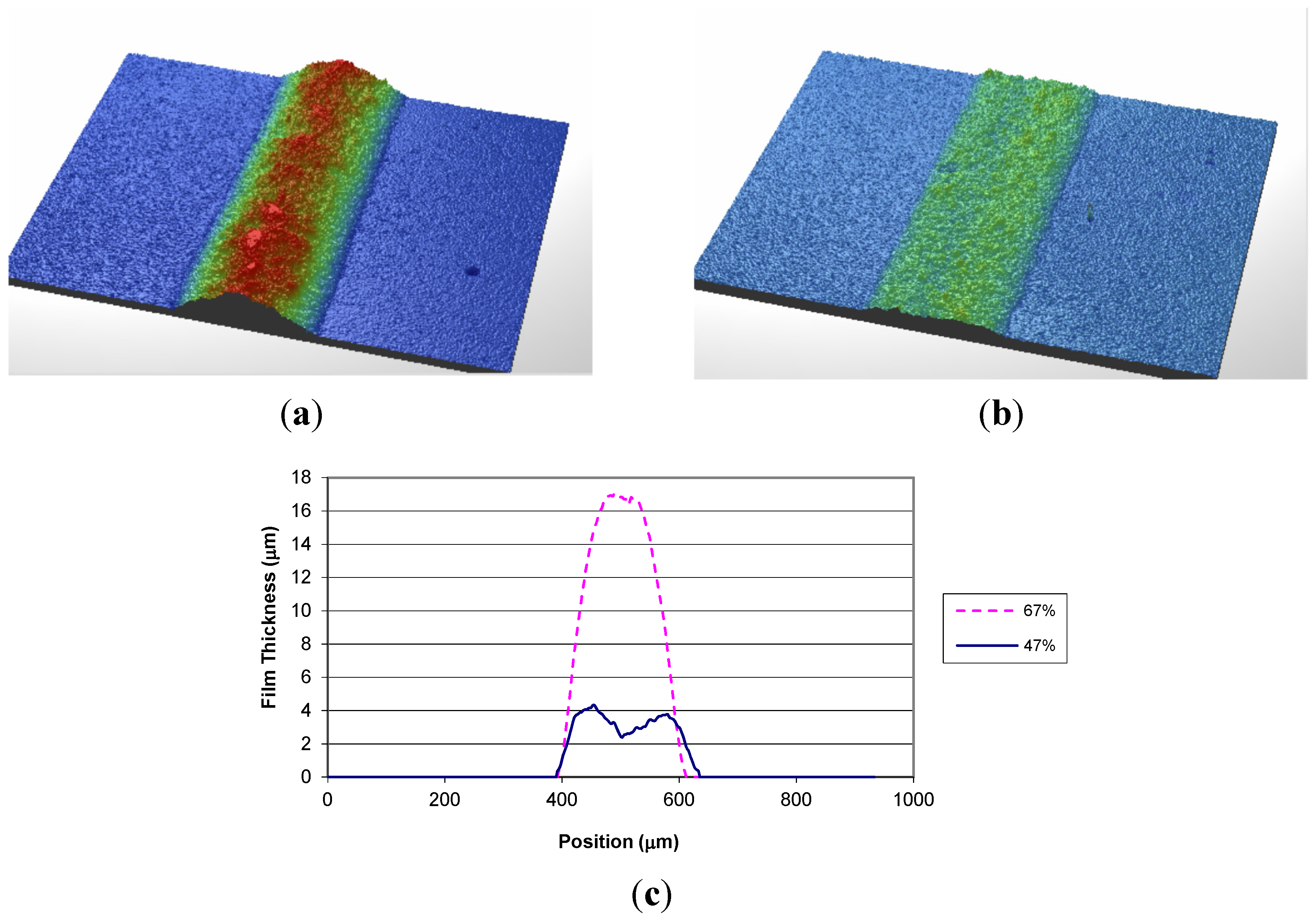
Table 1. One represents a traditional paste material used for rigid and flexible circuit printing while other is a novel polymer ink which has been developed for applications which are more cost sensitive.
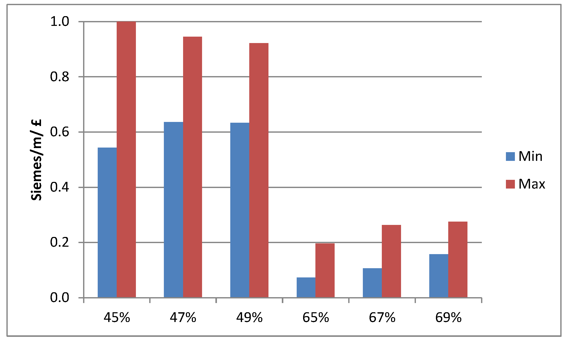
The polymer family of materials possesses a gel like consistency utilising a low silver content (between 45 wt.% and 49 wt.%) material in gel like binder/solvent. Usually such a low silver content would not produce such a conductive printed film as conductive percolation through the cured silver film could not be guaranteed. The gel binder used allows a greater solvent content without sacrificing rheological limits which subsequently leads to a more compact cured film than that which is achieved with conventional materials. Solids contents were measured using a Perkin Elmer TGA while volumetric calculations are based on the primary organic materials shown in manufacturer’s data [15,
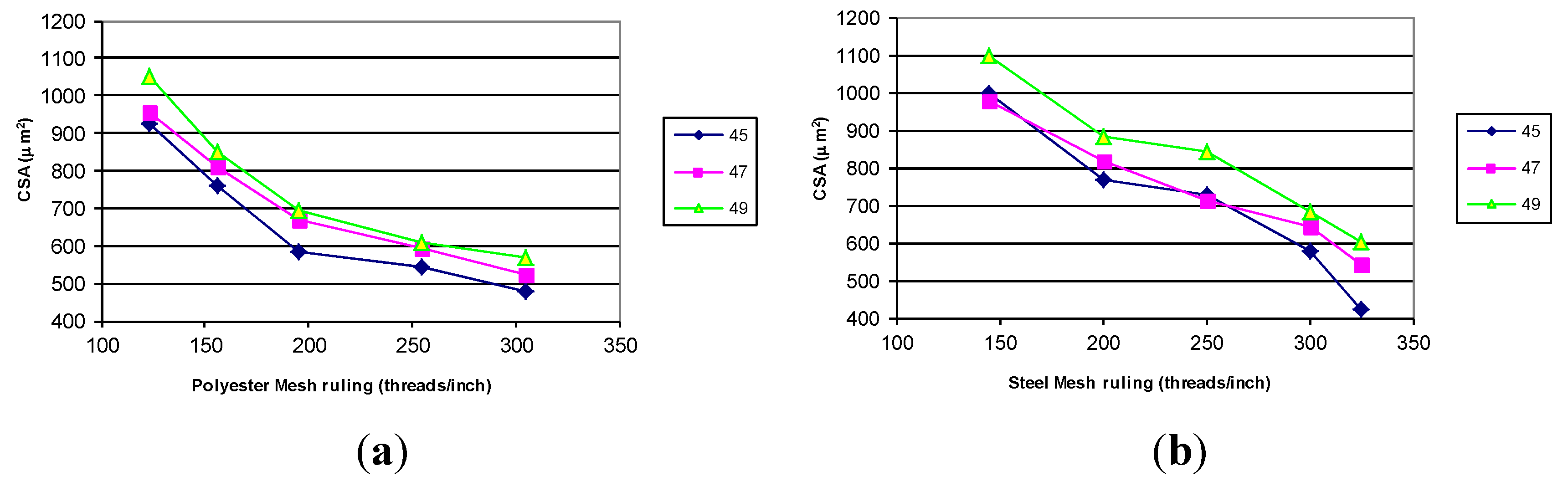
16] and standard densities for each component. From the densities and TGA, volumetric proportions for the wet and dry films can be calculated. Particle sizes were measured by SEM sections and plan views of the cured film. Analysis of the images was carried out using Image J software using visually assessed contrast enhancement (for edge detection) and blob analysis.
Table 1. Silver material properties.
NotationPolymerPaste
Material as provided
Ink silver content (wt.%)45, 47 and 4965, 67 and 69
Total solids (wt.%)51–5585–89
Dry film for each 1 μm wet (mid range material)0.1750.66
Dry film ratio for same wet film thickness13.8
As dried and printed (for the 47% and 67% materials respectively)
SEM of dry film Coatings 05 00172 i001 Coatings 05 00172 i002
Silver: Binder mass ratio7.8 : 13.4 : 1
Silver: Binder volume ratio0.7: 10.3 : 1
Mean particle size (μm)4.84.5
The exact formulation of the materials are not disclosed in the material datasheets and are subject to commercial confidentiality. For each formulation type the varying solids content was established by dispersing the silver within a binder/solvent mixture at maximum solids content, i.e., the maximum quantity of silver which could be added before the silver was no longer held in a stable homogenous suspension which was considered to within the viscosity range for the process. Solvent (butyl digol) was then added to individual batches of each base material at maximum silver concentration in a step wise manner in order to achieve the necessary silver content. Thus, within each formulation type each material differs only by the proportion of solvent in the formulation.
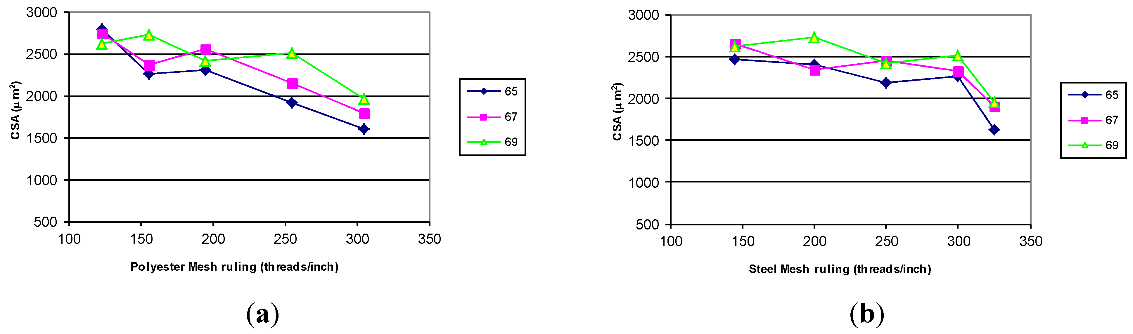
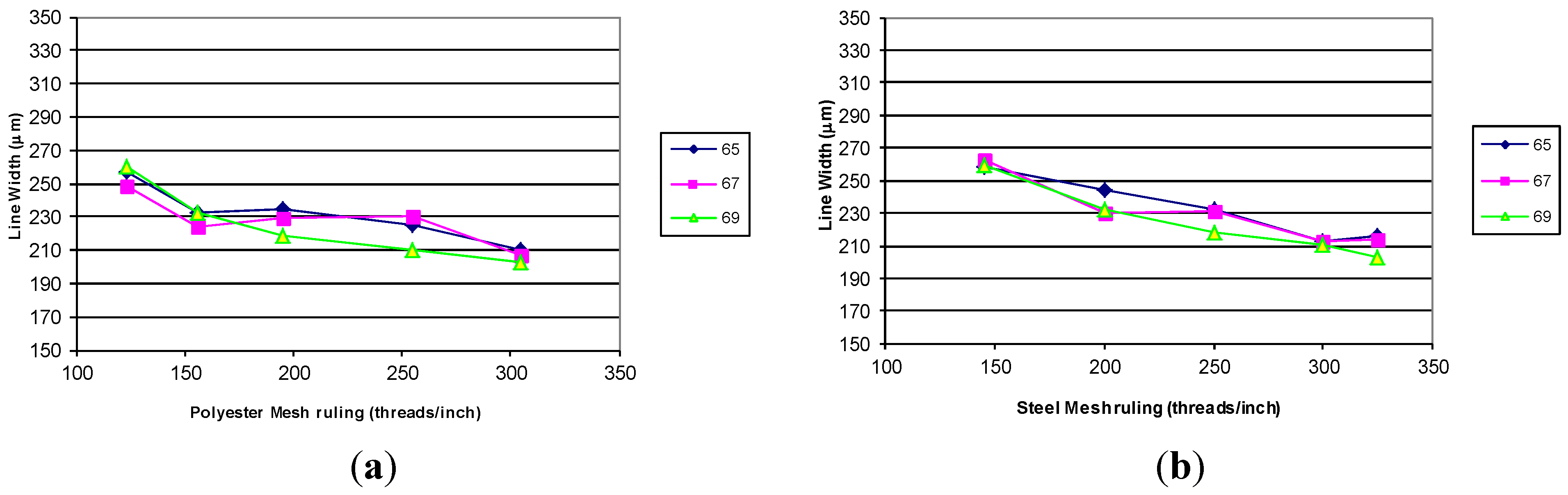
The film thickness in screen printing is predominantly dictated by the mesh characteristics of the screen [14]. Thus in order to examine the role of film thickness the materials were printed with 10 screens (5 polyester and 5 stainless steel). These screens represent the range of mesh rulings, and subsequent ink deposit, commonly used for screen printing conductive materials, Table 2. A nominal stencil thickness of 12 µm was used on all of the meshes and all screens were mounted with the mesh warp direction at 22.5° to the print direction.
A DEK 248 digitally controlled screen printing machine was used to print the experiment. This allows accurate and repeatable PC control settings to be applied to each experimental setup. Standard conditions were established for the printing which allowed deposition at each experimental condition. Six prints were produced at each experimental condition with any residual material being discarded. The screen and squeegee were cleaned within the press to ensure consistent set up. The materials were printed to 300 mm × 300 mm white stabilized PET substrate. The substrate was 250 μm thick with a Ra of 0.15 μm +/−0.02 μm.
Table 2. Mesh specifications.
MaterialMesh Ruling (threads/inch)Mesh ruling (threads/cm)Mesh opening (μm)Thread diameter (μm)Theoretical ink volume cm3/m2
Polyester123481337045
Polyester15661906430
Polyester19577774828
Polyester255100574021
Polyester305120453416
Stainless Steel145571185655
Stainless Steel20077904043
Stainless Steel25097633632
Stainless Steel300114563228
Stainless Steel325125503024
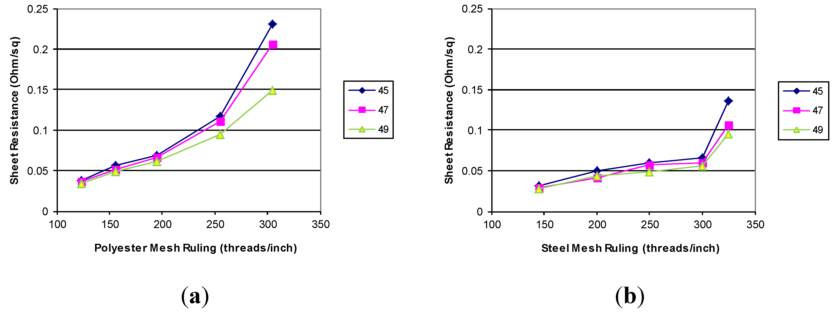
The prints were dried immediately after printing using a SC Technical hot air dryer at 120 °C with a residence time of 6 min. Of the six prints produced at each condition, samples 4, 5 and 6 were measured in order to reduce uncertainty. The printed design consisted of 30 mm long lines between 50 μm and 1000 μm in the print and transverse print direction. The results focus on the large solid area and cured 200 μm line which was reproduced consistently throughout the experiments and whose volume could be measured accurately. The sheet resistance was measured in a 50 mm × 50 mm solid layer section and were carried out using a Keithley 2400 source-meter operating in 4 point mode with a probe spacing of 5 mm with subsequent conversion to sheet resistance [17]. Each line resistance measurement represents an average of three measurements, while the sheet resistance represents an average of nine measurements.
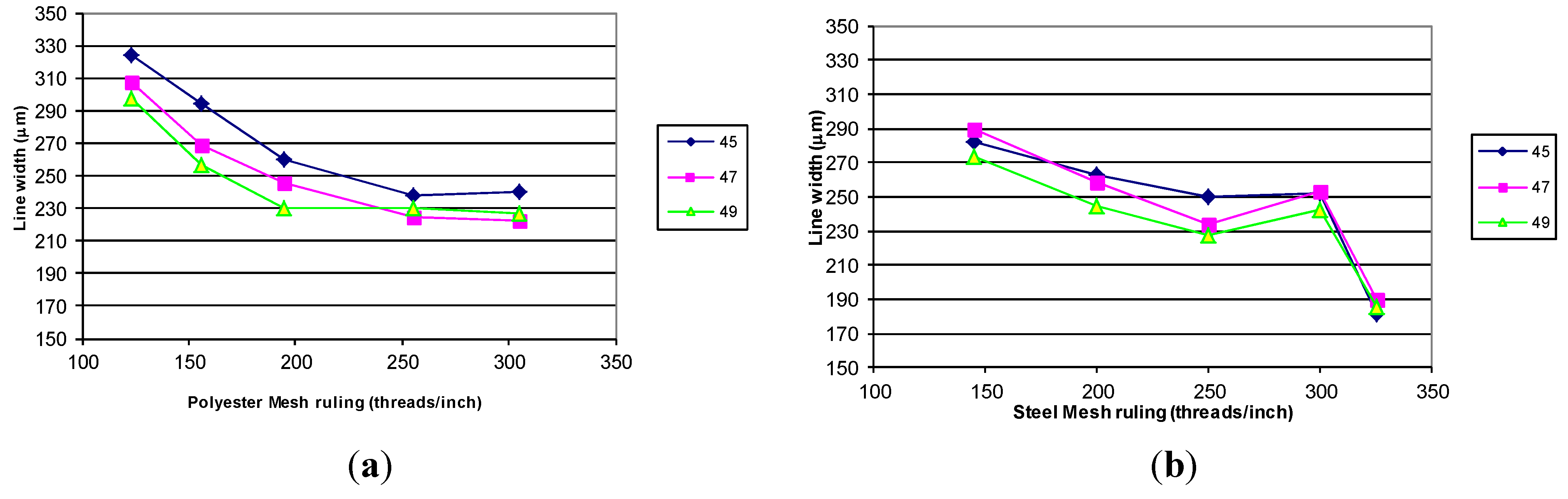
A Veeco NT 2000 White light interferometer was used to measure the printed line topology, width height and line volume. All measurements were carried out at ×5 optical resolution with a total vertical scan length of 30 μm. This yields a measurement area of 1.2 mm × 0.93 mm, sampling every 1.67 μm in the XY direction. The smooth nature of the substrate allowed clear reference surfaces on either side of the line, allowing the geometric characteristics and cross section of the line to be readily established. In order to take into account topological variations along the line length, mean characteristics were taken from each of the 480 pixels.
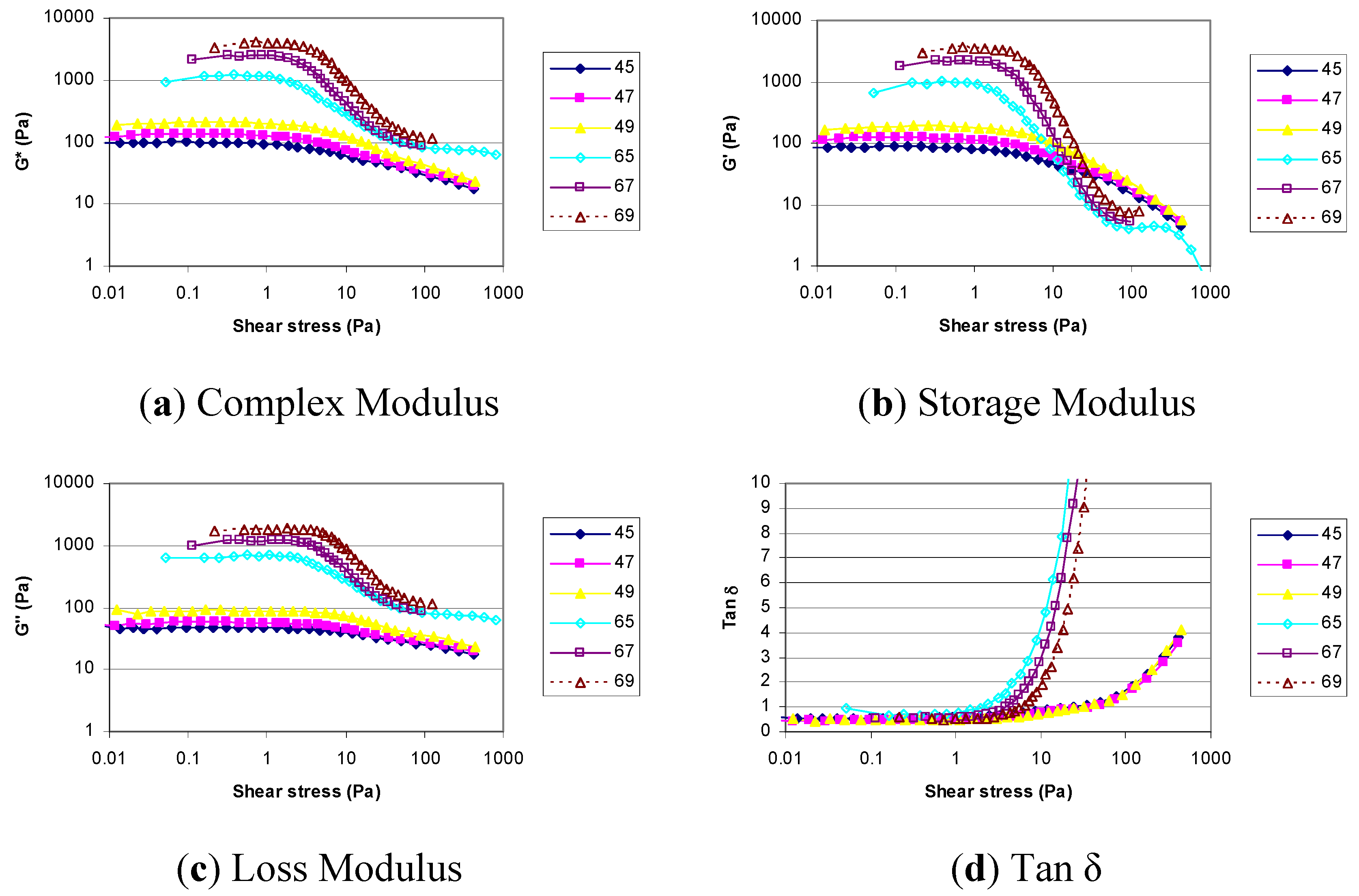
Material rheology was measured using a Bohlin Gemini HR nano rheometer. In order to examine the viscous and elastic properties of the ink at low shear a dynamic strain sweep with an angular frequency of 1 Hz was carried out. This technique was adopted as viscous and elastic behaviour at low shear has been postulated as a key indicator of the material transfer process [18] and the method adopted had shown important trends [14]. Measurements were carried out using a parallel plate geometry with a diameter of 20 mm and sample gap of 70 μm at 25 °C and were repeated three times for each material.

3. Results and Discussion

3.1. Material Rheology

Whilst the silver content and solvent/binder proportions are factors which determine the electrical and physical characteristics of the final cured printed structure, the physical action of the material transfer to the substrate is dictated by the rheology [10,14,18] Both materials possess highly pseudoplastic characteristics with a reduction in viscosity as the shear stress is increased, Figure 1a. The polymer material shows a gradual reduction in both elastic and loss modulus (and hence viscosity) with increasing applied stress with the liquid behaviour becoming dominant over solid behaviour at a shear stress between 10 and 100 Pa. The paste silver posseses a higher moduli at low shear stress followed by a rapid reduction in elastic moduli in the 1–10 Pa shear stress range resulting in the material exhibiting predominately liquid behaviour at a shear stress of 10 Pa. The most significant difference between the material sets is evident in the low stress behaviour of the traditional paste which possesses complex, storage and loss moduli which are at least an order of magnitude higher than the polymer material. The transition from solid to liquid dominated behaviour (as depicted by tan δ) is far more sudden for the paste inks and occurs at a shear stress which is an order of magnitude lower than the polymer material. For both materials, there is a step wise increase in elastic and viscous modulus as the silver content is increased. The impact of this formulation and rheology on electrical and physical characteristics of the print are presented later in the results.
Figure 1. Rheological characteristics for each silver material (a) viscosity over medium shear range, elastic (b) and viscous (c) modulii and (d) Tan δ.
Coatings 05 00172 g001

3.2. Printed Material Performance

As the materials have distinct performance in terms of rheology and printing performance, the presentation of the results will examine each material in turn before drawing comparisons between the material sets.

3.2.1. Polymer Inks

Increasing the mesh ruling resulted in a reduction sheet resistance as a result of the reduction in film thickness for the polymer inks, Figure 2. The sheet resistance is lower (typically less than 0.1 Ω/sq) for the stainless steel meshes at comparable mesh rulings as a result of the larger internal volume available within the mesh to contain the material. For both mesh types, the sheet resistance reduces as the silver content increases. For the stainless steel ink, there is a gradual increase as the mesh ruling increases and then shows a sudden increase with the 325 threads/cm mesh which has been attributed to the appearance of mesh patterning/marking in the printed solid film with this material. This topological surface phenomena is a result of a number of complex interacting parameters and is of importance to many applications [19].
Figure 2. The effect of mesh ruling on the polymer sheet resistance printed through the (a) polyester and (b) stainless steel meshes for each silver proportion.
Coatings 05 00172 g002
The cured cross sectional area effectively represents the total quantity of material transferred to the substrate once it is cured. This represents a more valid measurement than film thickness as it takes account non rectangular nature and topologically complex nature of the printed lines. For the polymer ink set, increasing the mesh ruling reduced the cross sectional area of the nominally 200 μm line for the polyester, Figure 3a, and steel meshes, Figure 3b. This reduction in ink in cross sectional area is in line with the reduction in available free volume within the mesh for material transfer. The volume reduction is around 50%–60% over the mesh ruling range investigated. For 49% silver this represents a reduction from 1100 μm2 to 560 μm2 while the 45% silver material reduces from 1000 μm2 to 425 μm2. The line cross sectional area with the lower silver content materials in line with the reduced solids content.
Figure 3. The effect of mesh ruling on the cured cross sectional area of the polymers inks for a nominally 200 μm line (a) polyester and (b) stainless steel meshes for each silver content.
Coatings 05 00172 g003
The line width is an important metric as it dictates feature density. The nominally 200 μm wide line is rendered wider than its nominal value for almost all mesh types, Figure 4. The lines are between 10 and 130 μm larger than nominal for the polyester mesh while the effect of the mesh ruling is less noticeable for the stainless steel screens. The increase in line width is most evident with the lowest solids material and reflects greater slumping of the lower viscosity material. There is a sudden reduction in printed line width at the highest mesh ruling, for the finest stainless steel screen which is attributed to a reduction in the overall film thickness (as shown by the cross sectional area in Figure 3b). This limits the quantity of wet material which slumps during the printing process. This tends to suggest that there is some minimum critical volume/height at which slumping does not occur.
Figure 4. The effect of mesh ruling on the cured printed line width of the polymers inks for a nominally 200 μm line (a) polyester and (b) stainless steel meshes for each silver content.
Coatings 05 00172 g004

3.2.2. Paste Inks

The paste inks show similar trends to the polymer ink in respect that the sheet resistance increases with mesh ruling, Figure 5. There is also a clear trend with a reduction in the sheet resistance as the silver content of the material is increased, Figure 5 Sheet resistances are approximately the same as those obtained with the polymer materials at coarse mesh rulings (around 0.05 Ω/sq).
Figure 5. The effect of mesh ruling on the paste sheet resistance printed through the (a) polyester and (b) stainless steel meshes for each silver proportion.
Coatings 05 00172 g005
The printed cross sectional area of the paste materials is significantly higher for the paste inks compared to the polymer inks with cross sectional areas ranging from 2800 μm2 to 1900 μm2 for the polyester mesh and 2500 μm2 to 1800 μm2 for the stainless steel mesh, Figure 6. For the paste inks, the cross sectional areas are higher for the stainless steel mesh than the comparable polyester mesh. The impact of the mesh ruling is less dramatic (typically reductions of 30% to 40%) than that observed with the polymer inks (Figure 3) where more proportional dramatic reductions in CSA were observed. There is a general trend that the cross section area is reduced for the lower silver content inks in line with reductions in solids content.
Figure 6. The effect of mesh ruling on the cured cross sectional area of the paste inks for a nominally 200 μm line (a) polyester and (b) stainless steel meshes.
Coatings 05 00172 g006
The impact of mesh ruling and solids content on the printed line width is less significant for the paste materials compared to the polymer materials, Figure 7. The line width increase is in the range of 10 and 50 μm larger than nominal and shows a gradual reduction as the mesh ruling increases although no clear trends are observed between the printed line width and the material solids content.
Figure 7. The effect of mesh ruling on the cured line width of the paste inks for a nominally 200 μm line (a) polyester and (b) stainless steel meshes.
Coatings 05 00172 g007

3.3. Comparison of Each Set of Materials

A clear difference between the between the two families is the cross sectional area (and hence film thickness) of the final cured film, Figure 8, which can be attributed to higher solids content in the paste materials. The polymer materials undergo a greater reduction in volume as the solvent content evaporates during the curing process. The polymer materials also exhibit a greater degree of line broadening with the lines consistently wider than that observed with the paste inks. This is attributed to the greater slumping of the lower viscosity material as it is released from the screen.
Figure 8. A comparison of the cross section of the printed lines through the polyester 195 threads/cm screen. (a) 3D view of 67% material; (b) 3D view of 47%; and (c) Mean cross section through line.
Coatings 05 00172 g008
From the measured cross sectional area and resistance of the 200 μm line, it is possible to calculate the printed material resistivity and hence conductivity. The thinner film produced with the polymer ink delivers a printed feature where the silver particles are more densely packed. The net result of the denser packing of the silver in the film is to increase the conductivity of the cured material, Figure 9. Within each material set there is a gradual increase in the conductance of the printed film as the silver proportion is increased. For the polymer materials, this varies between 2.2 × 10⁶ to 6.2 × 10⁶ S/m (between 15 and 37 times bulk resistivity) while the paste materials show a variation between 5 × 10⁵ and 1.6 × 10⁶ S/m (between 35 and 148 times bulk resistivity).
For each material family, increasing the film thickness increases the conductivity but there is some data spread. This spread is associated with a number of features of the printed lines. Irregularities along the line length, lead to islands of materials which contribute to the calculated cross sectional area but contribute nothing to the line conductivity. These topological variations are particularly visible with the polymer materials where films are thinner and where the effect of non continuous topographic anomalies are greater, Figure 10.
Figure 9. Spread of printed material conductivities obtained with each material/film thickness combination.
Coatings 05 00172 g009
Figure 10. Spread of material conductivities obtained with each material/film thickness combination.
Coatings 05 00172 g010
The increased conductivity of the polymer material demonstrates that it is possible to improve electrical performance by optimization of the binder system while maintaining a material which is capable of being processed in a conventional manner, i.e. the correct rheological and curing properties.
From commercial perspective, the relative merit of the materials and their universal applicability can be examined. A bill of materials (BOM) cost analysis of materials using data provided by the material supplier [15,16], shows that the dominant element of cost in the bill of materials is the silver, Table 3. The paste material (due to its higher silver content) has a 40% cost premium when compared to the polymer material. In practice, this premium is likely to lower as the manufacturing costs and operational overheads of the material supplier need also be considered.
Table 3. Cost analysis for bill of materials for the 47% and 67% silver content for each material family.
Component£/kgGel (@47% Ag)Paste (@67% Ag)
Silver metals costs232109154
Polymer 120.722.4
Solvent costs0.50.240.06
Total110158
An useful means of examining the commercial is to examine the conductivity (S/m) obtained per unit BOM currency which effectively describes the economic efficiency of the material, When this is normalised such that it is relevant to all currencies, the maximum conductivity/unit currency is given by the lowest silver content material (45%), Figure 11. The 45% material also however produces the largest range of values, highlighting that it produces lines where topological anomalies are increased. Thus, the lower silver materials provide a more cost effective conductive structure, they are more highly sensitive to the mesh being used as the printed films are thinner. This is also reflected in the range of line widths which are produced with the polymer materials. For the polymer materials, the range of the conductivity produced is narrower as the silver proportion is increased highlighting that there is a trade off between improved process robustness and material cost.
Figure 11. The range of conductivity/unit cost obtained with each material.
Coatings 05 00172 g011
The creation of this dataset linking feature silver material properties and screen characteristics has developed a design tool which can be used to determine the optimum material properties and process settings in order to achieve the desired electrical performance (and vice versa). Work on the inclusion of additional parameters such as squeegee settings, mesh tension, screen–substrate distance is on going such that these secondary parameters can be incorporated into the design tool. The dataset also serves to form the basis of cost models for material use given defined electrical requirements. A further factor which determines the screen which is to be used is the resolution of the image required with finer features requiring finer meshes to be used. The drive for finer features in order to reduce device size is thus dictating the use of finer meshes. An investigation into the relationship between mesh ruling, material properties and fine line rendering capabilities is on-going.

4. Conclusions

An experimental investigation has been carried out on the effect of screen printing silver material formulation and mesh type on the characteristics of printed conductive structures. The study has shown that it is possible to formulate large particle silver materials which can provide higher conductivities by increasing metal density in the cured film while maintaining materials within the operational window of the screen printing process. The thinner film nature of these new materials does however make them more prone to variations in printed resistance which will likely have an impact on product robustness. The impact of finer meshes is to reduce the printed film thickness which is in line with expectations but the degree to which the film thickness and sheet resistance is affected is dependent on the material being printed. Further studies will examine the role of other process parameters and printed features.

Acknowledgments

The authors would like to thank the Welsh Government and Gwent Electronic Materials for their support of this project.

Author Contributions

E.J. performed some of the experiments, analysis and primary authored the paper, S.H. performed the remainder of the experiments and analysis. T.C and D.G. drove the research programme, aided in experimental design and co-authored the work.

Conflicts of Interest

The authors declare no conflict of interest.

References

  1. Silver Inks and Pastes Markets: 2014–2021; N-tech Research: Glen Allen, VA, USA, 23 June 2014.
  2. Smith, P.J.; Shin, D.-Y.; Stringer, J.E.; Reis, N.; Derby, B. Direct inkjet printing and low temperature conversion of conductive silver patterns. J. Mater. Sci. 2006, 41, 4153–4158. [Google Scholar] [CrossRef]
  3. Sung, D.; de la Fuente Vornbrock, A.; Subramanian, V. Scaling and optimization of gravure-printed silver nanoparticle lines for printed electronics. IEEE Trans. Compon. Packag. Technol. 2010, 33, 105–114. [Google Scholar] [CrossRef]
  4. Deganello, D.; Cherry, J.A.; Gethin, D.T.; Claypole, T.C. Patterning of micro-scale conductive networks using reel-to-reel flexographic printing. Thin Solid Films 2010, 518, 6113–6116. [Google Scholar] [CrossRef]
  5. The Silver Inks and Pastes Market 2013; N-tech Research: Glen Allen, VA, USA, 7 January 2013.
  6. Owczarek, J.A.; Howland, F.L. A study of the off-contact screen printing process. I. Model of the printing process and some results derived from experiments. IEEE Trans. Compon. Hybrids Manuf. Technol. 1990, 13, 358–367. [Google Scholar] [CrossRef]
  7. Taroni, M.; Breward, C.J.W.; Howell, P.D.; Oliver, J.M.; Young, R.J.S. The screen printing of a power-law fluid. J. Eng. Math 2012, 73, 93–119. [Google Scholar] [CrossRef]
  8. Hoornstra, J.; Weeber, A.W.; de Moor, H.H.C.; Sinke, W.C. The Importance of Paste Rheology in Improving Fine Line, Thick Film Screen Printing of Front Side Metallization. In Proceedings of the 14th European Photovoltaic Solar Energy Conference (EPSEC), Barcelona, Spain, 1997; pp. 404–407.
  9. Hilali, M.M.; Nakayashiki, K.; Chandra, K.; Reedy, R.C.; Rohatgi, A.; Shaikh, A.; Kim, S.; Sridharan, S. Effect of Ag particle size in thick-film Ag paste on the electrical and physical properties of screen printed contacts and silicon solar cell. J. Electrochem. Soc. 2006, 153, A5–A11. [Google Scholar] [CrossRef]
  10. Lin, H.W.; Chang, C.P.; Hwu, W.H.; Ger, M.D. The rheological behaviours of screen-printing pastes. J. Mater. Process. Technol. 2008, 197, 284–291. [Google Scholar] [CrossRef]
  11. Buzby, D.; Dobie, A. Fine Line Screen Printing of Thick Film Pastes on Silicon Solar Cells. In Proceedings of the 41st International Symposium on Microelectronics (IMAPS 2008), Rhode Island, USA, 2–6 November 2008.
  12. Faddoul, R.; Reverdy-Bruas, N.; Blayo, A. Printing force effect on conductive silver tracks: Geometrical, surface, and electrical properties. J. Mater. Eng. Perform. 2012, 22, 640–649. [Google Scholar] [CrossRef]
  13. Merilampi, S.; Laine-Ma, T.; Ruuskanen, P. The characterization of electrically conductive silver ink patterns on flexible substrates. Microelectron. Reliab. 2009, 49, 782–790. [Google Scholar] [CrossRef]
  14. Jewell, E.H.; Hamblyn, S.M.; Claypole, T.C.; Gethin, D.T. The impact of carbon content and mesh on the characteristics of screen printed conductive structures. Circuit World 2013, 39, 3–21. [Google Scholar] [CrossRef]
  15. GEM–Conductive Silver Polymer Paste; Product information sheet provided by Gwent Electronic Materials. Available online: http://www.gwent.org/gem_data_sheets/polymer_systems_products/flexible_conductor_and_membrane_touch_switch/45_per_cent_ag_c2080415p2.pdf (accessed on 4 May 2015).
  16. GEM–Conductive Silver Ink; Product information sheet provided by Gwent Electronic Materials. Available online: http://www.gwent.org/gem_data_sheets/polymer_systems_products/flexible_conductor_and_membrane_touch_switch/65_per_cent_ag_c2110817d5.pdf (accessed on 4 May 2015).
  17. Smits, F.M. Measurement of sheet resistivites with 4 point probes. Bell System Tech. J. 1958, 37, 711–718. [Google Scholar] [CrossRef]
  18. Abbott, S.J.; Gaskell, P.H.; Kapur, N. A new model for the screen printing process—From theory to practical insight. In Proceedings of 2nd International Symposium on Printing & Coating Technology, Swansea, UK, September 2000.
  19. Petersen, I.; Hübner, G.; Claypole, T.C.; Jewell, E. Influence and interaction phenomena of screen printing machine settings on surface roughness. In Proceedings of International Association of Research Institutes for the Graphic Arts Industries (IARIGAI), Budapest & Debrecen, Hungary, 11–14 September 2011.

