
Reflective Meta-Films with Anti-Damage Property via Field Distribution Manipulation


1
Suzhou Institute of Nano-Tech and Nano-Bionics, Chinese Academy of Sciences, Suzhou 215125, China
2
Research Center of Laser Fusion, China Academy of Engineering Physics, Mianyang 621900, China
3
College of Science, Lanzhou University of Technology, Lanzhou 730050, China
4
Joint Laboratory for Extreme Conditions Matter Properties, Southwest University of Science and Technology, Mianyang 621010, China
*
Authors to whom correspondence should be addressed.
Coatings 2021, 11(6), 640; https://doi.org/10.3390/coatings11060640
Submission received: 23 April 2021
/
Revised: 23 May 2021
/
Accepted: 24 May 2021
/
Published: 27 May 2021
(This article belongs to the Special Issue Micro-Nano Optics and Its Applications)
Abstract
:The reflective optical multi-films with high damage thresholds are widely used in intense-light systems. Metasurfaces, which can manipulate light peculiarly, give a new approach to achieve highly reflective films by a single-layer configuration. In this study, reflective metasurfaces, composed of silicon nanoholes, are numerically investigated to achieve high damage thresholds. These nanoholes can confine the strongest electric field into the air zone, and, subsequently, the in-air electric field does not interact directly with silicon, attenuating the optothermal effect that causes damage. Firstly, the geometrical dependencies of silicon nanoholes’ reflectance and field distribution are investigated. Then, the excitation states of electric/magnetic dipoles in nanostructures are analyzed to explain the electromagnetic mechanism. Furthermore, the reflection dependences of the nanostructures on wavelength and incident angle are investigated. Finally, for a typical reflective meta-film, some optothermal simulations are conducted, in which a maximum laser density of 0.27 W/µm2 can be handled. The study provides an approach to improve the laser damage threshold of reflective nanofilms, which can be exploited in many intense-light applications.
1. Introduction
Metamaterials are artificial structural materials with many interesting properties not found in nature [1]. Among them, metasurfaces, which are composed of two-dimensional arrays of subwavelength nanostructures, have become a hotspot in the field of electromagnetic materials [2,3,4,5,6,7]. Metasurfaces have many exotic optical properties such as ultra-compact [8,9], perfect absorption [10,11], super-resolution [12,13,14], and large field of view [15,16], which have applications in miniaturization and integration of complex optical systems. After surface preparation, materials can still have enough strength and anti-corrosion [17,18]. In particular, the metasurfaces made of dielectrics have attracted much interest from researchers due to the advantages of low loss, thermal stability, magnetic effect, etc. [3,5]. Although some metasurfaces based on refractory materials such as HfO2, which have the application potentials in high-power systems, are reported [19,20], there is still no sufficient research on metasurfaces for high damage thresholds.
With the rapid development of intense-light systems, the complexity of optical systems based on traditional discrete elements rises sharply [21], which makes the cost of construction, operation, and maintenance increase dramatically. Thus, the miniaturization and integration of intense-light systems are urgently desirable. Due to the low threshold of bulk damages, the reflective components are wildly used in intense-light systems [22,23,24]. Among these elements, the highly reflective films with high damage thresholds are one of the most important parts. To obtain strong reflection, the traditional optical elements usually exploit complex multi-layer films with different dielectric constants to modulate light waves. Many methods have been exploited to seek high damage thresholds, such as using the femtosecond laser-induced damage threshold of e-beam-deposited reflective films [25] and tuning electric fields into air zones [26]. However, the multi-layer configuration suffers the disadvantages of structural complexity, thermal mismatch, and high cost [27,28]. According to the previous investigation, light-induced damages are caused mainly by the strong electric field, which excites damage precursors [26,29,30]. Anti-reflective coatings based on nanostructures are investigated [18,31], and the anti-damage feature has been obtained experimentally via manipulating a strong electric field into air zones [32]. In our previous work, the phase control of light reflected by the nanoholes with in-air confinement has been investigated for beam steering, and a meta-deflector with anti-damage properties was obtained [33]. Therefore, metasurfaces, which can manipulate electromagnetic fields in a subwavelength scale, can provide a new approach to address these issues of reflective films.
In this study, we proposed a reflective metasurface made of silicon nanoholes with high damage thresholds, which can confine a strong electric field into air zones. The in-air electric field does not interact directly with silicon, attenuating the optothermal effect that causes damage. Firstly, the geometrical dependencies of silicon nanoholes’ reflectance and field distribution are investigated. Then, the excitation states of the nanostructures are demonstrated to explain the electromagnetic mechanism insides. Furthermore, the reflection dependence of the nanostructures on wavelength and incident angle are investigated. Finally, the optothermal simulations are conducted to estimate the maximum laser density that the meta-films can handle. The nanohole configuration gives a new view for improving the laser damage threshold of other metasurfaces.
2. Materials and Methods
The studied metasurfaces are composed of a silicon film with nanoholes within a square lattice array on a silica substrate, as shown in Figure 1. The thickness of the silicon film is H = 200 nm, and the period of unit-cells is P = 600 nm. Each unit-cell possesses an ellipse nanohole with diameters Dx and Dy. Compared to the rectangular shape in our previous work [33], the ellipse has a smoother edge and lower surface energy, leading to weaker localized fields and better thermal stability. Compared to symmetrical structures such as nanocylinders, ellipses have one more parameter (i.e., D vs. Dx, Dy) to tune the field distribution inside. The incident light is an x-polarized plane wave, which is injected from the bottom of nanoholes and propagates along the z-axis direction. With different parameters, Dx and Dy, the reflectance and the distribution of the electromagnetic field can be tuned.
The optical properties of the nanoholes and meta-films are obtained by numerical simulations based on the finite-difference time-domain (FDTD) algorithm with the commercial software FDTD solutions 2018. The unit cells are surrounded by periodic boundaries in the x-axis and y-axis directions and perfectly matched layers (PML) in the z-axis direction. The optothermal simulations are based on the finite element method with the software Device 2018. The x-/y-axis boundaries were set as “closed”, and the z-axis boundaries were set as “shell”. The source and all objects were modeled as in Figure 1 and limited in the optical/optothermal simulation region. All the optical and thermal parameters of the materials came directly from the software’s databases.
3. Results
By tailing the parameters (diameters Dx and Dy) of nanoholes, the geometrical dependencies of silicon nanoholes’ reflectance and field distribution are calculated via electromagnetic simulations. When H = 200 nm, and P = 600 nm, the reflectance of incident light with wavelength 1064 nm is reported as a function of Dx and Dy, as shown in Figure 2. It is seen that a high reflectance peak of 99.48% appears at Dx = 0.485 µm and Dy = 0.525 µm. To illustrate the electromagnetic mechanism of high damage thresholds, the electric field distributions at this reflectance peak (marked in Figure 2b) are shown in Figure 3. The strong electric field is manipulated in the air hole, the edge of which is marked by the black curves. The results show that the strongest electric field can be tuned into the air nanoholes while the perfect reflection appears. It means that the in-air electric field does not interact with silicon directly, attenuating the optothermal effect and temperature increase when illuminated by intense light.
To explain the mechanism of the perfect reflection, the electromagnetic excitation states of the nanoholes are analyzed. For the marked reflection peak in Figure 2, the electric/magnetic field distributions are presented in Figure 4. The white arrows show the direction and intensity of the electromagnetic vector on the x-z plane/y-z plane. The electric field concentrates in the air hole while the magnetic field mainly locates in silicon. It is seen that the electric field is parallel in the nanohole while the magnetic field distributes as an untypical vortex. This is the feature of an electric dipole that is mixed up with a weak magnetic dipole [9]. Therefore, the high reflectance is dominated by the electric dipole. The coupling effect between the electric dipoles of the nanoholes in lattice can greatly increase the reflectance with photonic crystal radiation [34,35].
Due to the resonance effect, the wavelength dependence of the nanoholes is obvious, as shown in Figure 5. When Dx is constant 0.485 µm, the reflectance is reported as a function of wavelength and Dy in Figure 5a. Here, the heights of nanoholes are constant H = 200 nm, and the lattice period P is 600 nm. There are two strips of high reflection, and they intersect with each other at the position of Dy = 0.47 µm. The dispersion property of the reflection is shown in Figure 5b with Dy = 0.35 µm and 0.54 µm, which are marked by the white dash line in Figure 5a. There are three perfect reflection peaks of 99.33%, 99.68%, and 98.71% at the wavelengths 1.075 µm, 1.16 µm, and 1.305 µm, respectively.
To illustrate the electromagnetic mechanism of the reflection with the in-air electric field, the distributions of the electric/magnetic field in the nanohole with Dx = 0.485 µm and Dy = 0.35 µm are shown in Figure 6. The white arrows indicate the direction and intensity of the electromagnetic vector on the x-z plane/y-z plane. For the reflection peak at 1.16 µm, the electric field concentrates in silicon and shows a vortex feature. At the same time, the magnetic field concentrates in the Si film, and the field vectors are parallel in the air nanohole. Therefore, the corresponding resonance of the peak at 1.16 µm is a magnetic dipole. For the peak at 1.305 µm, the electromagnetic fields show an oppositive feature. The electric field concentrates in the air hole with the parallel vector direction while the magnetic field is confined in silicon with a vortex feature, which is a typical magnetic dipole. Although both the electric/magnetic dipoles can produce reflection with very high efficiency, the magnetic-dipole-caused reflection does not have a high damage threshold due to the in-silicon confinement of electric fields. When the two strips of high reflection connect, the state is a mix of the electric/magnetic dipoles. The electromagnetic excitation state in Figure 4 and the peak at = 1.075 µm of the brown curve in Figure 5b belong to this case.
As a highly reflective film, the incident-angle dependence of reflectance is very important in applications. Here, this dependence is investigated with different angles during the 0°–30° range, as shown in Figure 7. The reflectance falls dramatically from 99.8% to 6.9% when the angle changes from 0° to 6°, meaning a high sensitivity of the incident angle [36].
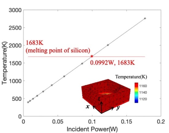
The electric field distribution only shows the anti-damage potential of the meta-film qualitatively. For quantitative analysis, some optothermal simulations are conducted to estimate the maximum laser intensity that the meta-film can handle. Figure 8a shows the temperature distribution in the unit-cell (area: 0.36 µm2) of the meta-film illustrated by a plane-wave laser with power 0.0625 W. The unit cells have a similar temperature value, from 1120 K to 1160 K. Under the illumination of different incident powers, the maximum temperature values in the 3D volume of the unit cell are reported in Figure 8b. The melting point of silicon is 1683 K. It is shown that the meta-film can handle the maximum laser power (0.0992 W per 0.36 µm2), i.e., the laser density of 0.27 W/µm2. This power value is higher than that (0.24 W/µm2) in our previous work of meta-deflectors [33].
4. Conclusions
In this study, reflective meta-films, made of silicon nanoholes, are investigated to obtain high damage thresholds via tuning the distribution of the electric field. The simulation results show that the strongest electric fields can be tuned into the air nanoholes with a high reflectance above 99%, attenuating the optothermal effect. The analysis of the excitation states demonstrated that the strong reflection with in-air-hole fields stems from the electric dipole, not the magnetic dipole. This design principle can be exploited into other nanohole metasurfaces for obtaining anti-damage properties. The reflectance of meta-films is very sensitive to incident angle, which can drop dramatically from 99.8% to 6.9% when the angle changes from 0° to 6°. The meta-films can be used as optical switches dependent on angle. The optothermal simulations show that the meta-film can handle a maximum laser density of 0.27 W/µm2, which is higher than the value of 0.24 W/µm2 in our previous work of meta-deflectors. Because the narrowest width of the meta-film is 72 nm, the e-beam lithography or other ultra-precise methods are necessary for fabrication, and the cost of large meta-films for intense light should be considered. In sum, the study provides an ingenious approach to obtain reflective meta-films with high damage thresholds, which can be used in the intense-light optical systems, instead of their multilayer counterparts. They have many potential applications in laser scalpels, laser cutting devices, etc.
Author Contributions
Conceptualization, F.T. and Y.W.; methodology, H.Y.; software, J.C.; investigation, H.Y.; resources, X.Y. and Z.Y.; writing—original draft preparation, H.Y. and F.T; writing—review and editing, H.Y.; supervision, Y.W. and F.T.; funding acquisition, H.Y., F.T., X.Y. and Z.Y. All authors have read and agreed to the published version of the manuscript.
Funding
This research was funded by National Natural Science Foundation of China, grant No. [61705204,61705206]; China Postdoctoral Science Foundation, grant No. [2019M653486, 2019M651998]; Innovation and Development Foundation of China Academy of Engineering Physics, grant No. [CX20200021]; Natural Science Foundation of Jiangsu Province, grant No. [BK20190229]; Scientific Research Fund of Sichuan Provincial Science and Technology Department, grant No. [2020YJ0137].
Institutional Review Board Statement
Not applicable.
Informed Consent Statement
Not applicable.
Data Availability Statement
Not applicable.
Conflicts of Interest
The authors declare no conflict of interest.
References
- Cui, T.J.; Smith, D.R.; Liu, R. Metamaterials; Springer: Berlin/Heidelberg, Germany, 2010. [Google Scholar]
- Zhang, L.; Mei, S.; Huang, K.; Qiu, C.-W. Advances in Full Control of Electromagnetic Waves with Metasurfaces. Adv. Opt. Mater. 2016, 4, 818–833. [Google Scholar] [CrossRef]
- Jahani, S.; Jacob, Z. All-dielectric metamaterials. Nat. Nanotechnol. 2016, 11, 23. [Google Scholar] [CrossRef]
- Glybovski, S.B.; Tretyakov, S.A.; Belov, P.A.; Kivshar, Y.S.; Simovski, C.R. Metasurfaces: From microwaves to visible. Phys. Rep. 2016, 634, 1–72. [Google Scholar] [CrossRef]
- Genevet, P.; Capasso, F.; Aieta, F.; Khorasaninejad, M.; Devlin, R. Recent advances in planar optics: From plasmonic to dielectric metasurfaces. Optica 2017, 4, 139–152. [Google Scholar] [CrossRef]
- Hou-Tong, C.; Antoinette, J.T.; Nanfang, Y. A review of metasurfaces: Physics and applications. Rep. Prog. Phys. 2016, 79, 076401. [Google Scholar]
- Chu, P.; Chen, J.; Xiong, Z.; Yi, Z. Controllable frequency conversion in the coupled time-modulated cavities with phase delay. Opt. Commun. 2020, 476, 126338. [Google Scholar] [CrossRef]
- Faraji-Dana, M.; Arbabi, E.; Arbabi, A.; Kamali, S.M.; Kwon, H.; Faraon, A. Compact folded metasurface spectrometer. Nat. Commun. 2020, 9, 4196. [Google Scholar] [CrossRef]
- Shalaev, M.I.; Sun, J.; Tsukernik, A.; Pandey, A.; Nikolskiy, K.; Litchinitser, N.M. High-Efficiency All-Dielectric Metasurfaces for Ultracompact Beam Manipulation in Transmission Mode. Nano Lett. 2015, 15, 6261–6266. [Google Scholar] [CrossRef] [Green Version]
- Xia, Z.; Qin, X.; Wu, Y.; Pan, Y.; Zhou, J.; Zhang, Z. Efficient broadband light absorption in elliptical nanohole arrays for photovoltaic application. Opt. Lett. 2015, 40, 5814–5817. [Google Scholar] [CrossRef]
- Yu, P.; Yang, H.; Chen, X.; Yi, Z.; Yao, W.; Chen, J.; Yi, Y.; Wu, P. Ultra-wideband solar absorber based on refractory titanium metal. Renew. Energy 2020, 158, 227–235. [Google Scholar] [CrossRef]
- Arbabi, A.; Horie, Y.; Bagheri, M.; Faraon, A. Dielectric metasurfaces for complete control of phase and polarization with subwavelength spatial resolution and high transmission. Nat. Nanotechnol. 2015, 10, 937. [Google Scholar] [CrossRef] [Green Version]
- Khorasaninejad, M.; Chen, W.T.; Devlin, R.C.; Oh, J.; Zhu, A.Y.; Capasso, F. Metalenses at visible wavelengths: Diffraction-limited focusing and subwavelength resolution imaging. Science 2016, 352, 1190–1194. [Google Scholar] [CrossRef] [PubMed] [Green Version]
- Khorasaninejad, M.; Chen, W.T.; Oh, J.; Capasso, F. Super-Dispersive Off-Axis Meta-Lenses for Compact High Resolution Spectroscopy. Nano Lett. 2016, 16, 3732–3737. [Google Scholar] [CrossRef]
- Pu, M.; Li, X.; Guo, Y.; Ma, X.; Luo, X. Nanoapertures with ordered rotations: Symmetry transformation and wide-angle flat lensing. Opt. Express 2017, 25, 31471–31477. [Google Scholar] [CrossRef] [PubMed]
- Hail, C.U.; Poulikakos, D.; Eghlidi, H. High-Efficiency, Extreme-Numerical-Aperture Metasurfaces Based on Partial Control of the Phase of Light. Adv. Opt. Mater. 2018, 6, 1800852. [Google Scholar] [CrossRef] [Green Version]
- Rodríguez-Barrero, S.; Fernández-Larrinoa, J.; Azkona, I.; de Lacalle, L.L.; Polvorosa, R. Enhanced performance of nanostructured coatings for drilling by droplet elimination. Mater. Manuf. Process. 2016, 31, 593–602. [Google Scholar] [CrossRef]
- Ray, N.J.; Yoo, J.H.; Nguyen, H.T.; Johnson, M.A.; Feigenbaum, E. Substrate-engraved antireflective nanostructured surfaces for high-power laser applications. Optica 2020, 7, 516–526. [Google Scholar] [CrossRef]
- Zhang, C.; Divitt, S.; Fan, Q.; Zhu, W.; Agrawal, A.; Xu, T.; Lezec, H.J. All-dielectric Deep Ultraviolet Metasurfaces. In CLEO: QELS_Fundamental Science 2019; Optical Society of America: New York, NY, USA, 2019; p. FM3C.3. [Google Scholar]
- Tang, F.; Ye, X.; Li, Q.; Li, H.; Yu, H.; Wu, W.; Li, B.; Zheng, W. Quadratic Meta-Reflectors Made of HfO2 Nanopillars with a Large Field of View at Infrared Wavelengths. Nanomaterials 2020, 10, 1148. [Google Scholar] [CrossRef] [PubMed]
- Moses, E.I.; Lindl, J.D.; Spaeth, M.L.; Patterson, R.W.; Sawicki, R.H.; Atherton, L.J.; Baisden, P.A.; Lagin, L.J.; Larson, D.W.; MacGowan, B.J. Overview: Development of the National Ignition Facility and the Transition to a User Facility for the Ignition Campaign and High Energy Density Scientific Research. Fusion Sci. Technol. 2016, 69, 1–24. [Google Scholar] [CrossRef]
- Rakickas, T.; Kudriašov, V.; Sirutkaitis, V.; Grigonis, R.; Gaižauskas, E. Evaluation of self-focusing influence on laser-induced damage threshold of anti-reflective coated windows. In Laser-Induced Damage in Optical Materials: 2005; International Society for Optics and Photonics: Bellingham, WA, USA, 2006; Volume 5991, p. 59911J. [Google Scholar]
- Papandrew, A.; Stolz, C.J.; Wu, Z.; Loomis, G.E.; Falabella, S. Laser conditioning characterization and damage threshold prediction of hafnia/silica multilayer mirrors by photothermal microscopy. In Laser-Induced Damage in Optical Materials: 2000; International Society for Optics and Photonics: Bellingham, WA, USA, 2001; Volume 4347, pp. 53–61. [Google Scholar]
- Gallais, L. Laser Damage of reflective optics in the sub-ps regime: Physical mechanisms and technological issues. In Laser Applications Conference 2019; Optical Society of America: New York, NY, USA, 2019; p. CM2C.3. [Google Scholar]
- Hervy, A.; Chériaux, G.; Gallais, L.; Mouricaud, D.; Djidel, S. Femtosecond laser-induced damage threshold of electron-beam deposited materials for broadband high-reflective coatings on large optics. In Pacific Rim Laser Damage 2014: Optical Materials for High-Power Lasers; International Society for Optics and Photonics: Bellingham, WA, USA, 2014; Volume 9238, p. 92380A. [Google Scholar]
- Li, C.; Sun, Y.; Song, X.; Zhang, X.; Shi, Z.; Wang, F.; Ye, X.; Chen, S.; Sun, L.; Huang, J. Capping a glass thin layer on the etched surface via plasma chemical vapor deposition for improving the laser damage performance of fused silica. Opt. Express 2019, 27, 2268–2280. [Google Scholar] [CrossRef]
- Li, Y.; Liu, Y.; Dai, H.; Zhang, X.; Luo, D.; Sun, X. Flexible cholesteric films with super-reflectivity and high stability based on a multi-layer helical structure. J. Mater. Chem. C 2017, 5, 10828–10833. [Google Scholar] [CrossRef]
- Hamamoto, K.; Shoki, T.; Ikebe, Y. Substrate Equipped with Multi-Layer Reflection Film, Reflection-Type Mask Blank, reflection-Type Mask, and Semiconductor Device Manufacturing Process. U.S. Patent Application No. 16/754,306, 1 October 2020. [Google Scholar]
- Manes, K.; Spaeth, M.; Adams, J.; Bowers, M. Damage Mechanisms Avoided or Managed for NIF Large Optics. Fusion Sci. Technol. 2016, 69, 146–249. [Google Scholar] [CrossRef]
- Laixi, S.; Jin, H.; Hongjie, L.; Xin, Y.; Jingjun, W.; Xiaodong, J.; Liming, Y.; Wanguo, Z.; Weidong, W. Combination of reaction ion etching and dynamic chemical etching for improving laser damage resistance of fused silica optical surfaces. Opt. Lett. 2016, 41, 4464. [Google Scholar]
- Pickering, T.; Shanks, K.; Sundaram, S. Modelling technique and analysis of porous anti-reflective coatings for reducing wide angle reflectance of thin-film solar cells. J. Opt. 2021, 23, 025901. [Google Scholar] [CrossRef]
- Ye, X.; Hu, X.; Tang, F.; Wu, J.; Yang, L.; Huang, J.; Zheng, W. Laser Field Manipulation and Laser Damage Resistance Property of Nanotextures on Fused Silica Optics. Results Phys. 2020, 18, 103262. [Google Scholar] [CrossRef]
- Yu, H.; Tang, F.; Wu, J.; Yi, Z.; Ye, X.; Wang, Y. Meta-Deflectors Made of Dielectric Nanohole Arrays with Anti-Damage Potential. Photonics 2021, 8, 107. [Google Scholar] [CrossRef]
- Sun, S.; Zhou, Z.; Zhang, C.; Gao, Y.; Duan, Z.; Xiao, S.; Song, Q. All-Dielectric Full-Color Printing with TiO2 Metasurfaces. ACS Nano 2017, 11, 4445–4452. [Google Scholar] [CrossRef] [PubMed]
- Cho, E.-H.; Kim, H.-S.; Cheong, B.-H.; Oleg, P.; Xianyua, W.; Sohn, J.-S.; Ma, D.-J.; Choi, H.-Y.; Park, N.-C.; Park, Y.-P. Two-dimensional photonic crystal color filter development. Opt. Express 2009, 17, 8621–8629. [Google Scholar] [CrossRef] [PubMed]
- Born, N.; Schneider, L.; Balzer, J.; Al-Naib, I.; Singh, R.; Velauthapillai, A.; Scheller, M.; Moloney, J.V.; Koch, M. Multi-band metamaterials with a distinguished angular sensitivity. In Proceedings of the 2015 40th International Conference on Infrared, Millimeter, and Terahertz Waves (IRMMW-THz), Hong Kong, China, 23–28 August 2015; IEEE: New York, NY, USA, 2015; pp. 1–2. [Google Scholar]
Figure 1.
Schematic of silicon nanoholes on a silica substrate with diameters Dx, Dy, thickness H, and lattice period P. The illumination is injected into the nanohole from the bottom.
Figure 1.
Schematic of silicon nanoholes on a silica substrate with diameters Dx, Dy, thickness H, and lattice period P. The illumination is injected into the nanohole from the bottom.

Figure 2.
Reflectance of Si nanoholes: (a) Reflectance as a function of Dx and Dy; (b) Reflectance as a function of Dy when Dx = 0.485 µm. Here, the heights of the nanoholes are constant H = 200 nm, and the lattice period P is 600 nm.
Figure 2.
Reflectance of Si nanoholes: (a) Reflectance as a function of Dx and Dy; (b) Reflectance as a function of Dy when Dx = 0.485 µm. Here, the heights of the nanoholes are constant H = 200 nm, and the lattice period P is 600 nm.

Figure 3.
Electric field distributions of the reflection peak marked in Figure 2b: (a) Normalized electric field distribution on the x-y plane with z = 100 nm; (b) Normalized electric field distribution on the x-z plane with y = 0.
Figure 3.
Electric field distributions of the reflection peak marked in Figure 2b: (a) Normalized electric field distribution on the x-y plane with z = 100 nm; (b) Normalized electric field distribution on the x-z plane with y = 0.

Figure 4.
Electric/Magnetic field distributions of the reflection peak marked in Figure 2b: (a) Normalized electric field distribution on the x-z plane with y = 0; (b) Normalized magnetic field distribution on the y-z plane with x = 0.
Figure 4.
Electric/Magnetic field distributions of the reflection peak marked in Figure 2b: (a) Normalized electric field distribution on the x-z plane with y = 0; (b) Normalized magnetic field distribution on the y-z plane with x = 0.

Figure 5.
Dispersion of Si nanoholes: (a) Reflectance as a function of wavelength and Dy. (b) Reflectance when Dy equals 0.35 µm and 0.54 µm, which is marked by the white dash line in (a). Here, the heights of nanoholes are constant H = 200 nm, Dx=0.485 µm, and the lattice period P is 600 nm.
Figure 5.
Dispersion of Si nanoholes: (a) Reflectance as a function of wavelength and Dy. (b) Reflectance when Dy equals 0.35 µm and 0.54 µm, which is marked by the white dash line in (a). Here, the heights of nanoholes are constant H = 200 nm, Dx=0.485 µm, and the lattice period P is 600 nm.

Figure 6.
Electric/Magnetic field distributions of the reflection peaks marked in Figure 5b: (a) Normalized electric field distribution at λ = 1.16 µm on the x-z plane with y = 0; (b) Normalized magnetic field distribution at λ = 1.116 µm on the y-z plane with x = 0. (c) Normalized electric field distribution of λ = 1.305 µm on the x-z plane with y = 0; (d) Normalized magnetic field distribution of λ = 1.305 µm on the y-z plane with x = 0.

Figure 7.
Reflection of Si nanoholes as a function of incident angle. Here, the height H = 200 nm, Dx = 0.485 µm, Dy = 0.43 µm, and the lattice period P is 600 nm.
Figure 7.
Reflection of Si nanoholes as a function of incident angle. Here, the height H = 200 nm, Dx = 0.485 µm, Dy = 0.43 µm, and the lattice period P is 600 nm.

Figure 8.
Photothermal analysis of the reflective meta-film: (a) the temperature distribution in the unit-cell (area: 0.36 µm2) of the meta-film illustrated by a plane-wave laser with power 0.0625 W; (b) the maximum value of temperature in the 3D volume of the unit-cell (a) under the illumination of different incident powers. Here, the height H = 200 nm, Dx = 0.485 µm, Dy = 0.525 µm, and the lattice period P is 600 nm.

Publisher’s Note: MDPI stays neutral with regard to jurisdictional claims in published maps and institutional affiliations. |
© 2021 by the authors. Licensee MDPI, Basel, Switzerland. This article is an open access article distributed under the terms and conditions of the Creative Commons Attribution (CC BY) license (https://creativecommons.org/licenses/by/4.0/).
Share and Cite
MDPI and ACS Style
Yu, H.; Tang, F.; Chen, J.; Yi, Z.; Ye, X.; Wang, Y. Reflective Meta-Films with Anti-Damage Property via Field Distribution Manipulation. Coatings 2021, 11, 640. https://doi.org/10.3390/coatings11060640
AMA Style
Yu H, Tang F, Chen J, Yi Z, Ye X, Wang Y. Reflective Meta-Films with Anti-Damage Property via Field Distribution Manipulation. Coatings. 2021; 11(6):640. https://doi.org/10.3390/coatings11060640
Chicago/Turabian StyleYu, Haichao, Feng Tang, Jun Chen, Zao Yi, Xin Ye, and Yiqun Wang. 2021. "Reflective Meta-Films with Anti-Damage Property via Field Distribution Manipulation" Coatings 11, no. 6: 640. https://doi.org/10.3390/coatings11060640
Note that from the first issue of 2016, this journal uses article numbers instead of page numbers. See further details here.