Article

Design of Narrow-Band Absorber Based on Symmetric Silicon Grating and Research on Its Sensing Performance

1
College of Physics and Information Engineering, Quanzhou Normal University, Quanzhou 362000, China
2
College of Chemical Engineering and Materials Science, Quanzhou Normal University, Quanzhou 362000, China
3
College of Electronics and Information Science, Fujian Jiangxia University, Fuzhou 350108, China
4
School of Mechanical and Electrical Engineering, Putian University, Putian 351100, China
*
Author to whom correspondence should be addressed.
Coatings 2021, 11(5), 553; https://doi.org/10.3390/coatings11050553
Submission received: 24 February 2021 / Revised: 17 April 2021 / Accepted: 19 April 2021 / Published: 8 May 2021
(This article belongs to the Special Issue Micro-Nano Optics and Its Applications)

Abstract

:
In this paper, using the surface plasmon and Fabry–Pérot (FP) cavity, the design of a symmetric silicon grating absorber is proposed. The time-domain finite difference method is used for simulation calculations. The basic unit structure is a dielectric grating composed of silicon dioxide, metal and silicon. Through the adjustment of geometric parameters, we have achieved the best of the symmetric silicon grating absorber. A narrowband absorption peak with an absorption rate greater than 99% is generated in the 3000–5000 nm optical band, and the wavelength of the absorption peak is λ = 3750 nm. The physical absorption mechanism is that silicon light generates surface plasmon waves under the interaction with incident light, and the electromagnetic field coupling of surface plasmon waves and light causes surface plasmon resonance, thereby exciting strong light response modulation. We also explore the influence of geometric parameters and polarization angle on the performance of silicon grating absorbers. Finally, we systematically study the refractive index sensitivity of these structures. These structures can be widely used in optical filtering, spectral sensing, gas detection and other fields.

1. Introduction

In recent years, the resonance phenomenon of nanostructures has been widely studied in periodic structures. The resonance mode can be excited by surface plasmon or photon, which affects the absorption characteristics of the structure [1,2,3,4]. Among them, the ideal absorber with a wide working wavelength is very useful in photon detection and light energy absorption [5,6,7], while the ideal absorber with narrow working bandwidth has great advantages in sensing, filtering and selective thermal radiation [8,9,10,11,12,13,14,15]. The refractive index (RI) sensors based on perfect narrowband wave absorbers have broad application prospects because of their simple construction and high sensitivity [16,17,18,19,20,21]. Researchers have proposed such a sensor with good performance [22,23]. In addition, photothermal detection can also be realized by a narrowband ideal absorber [24].
To obtain narrowband perfect absorbers, many people have studied all-metal structures or three-layer or multi-layer metal insulator metal (MIM) structures [25,26,27,28,29,30]. However, they are not compatible with the complementary metal-oxide-semiconductor (CMOS) process and have high manufacturing costs [31]. Therefore, people are paying attention to the realization of narrowband perfect absorbers through the dielectric structure on the metal system [32,33,34]. Compared with the perfect metal absorber, this absorber can save manufacturing costs [35]. More important, it can avoid complicated lithography processes. To produce ultra-narrow absorption, we usually insert a dielectric layer between grating and metal. However, the structure is relatively complex. Therefore, to simplify the structure, we can place the dielectric on top of the metal substrate [36,37,38,39,40]. For example, Fitio et al. systematically studied the perfect absorption spectrum of dielectric grating on metal structure [41]. Later, Liao et al. proposed a narrowband perfect wave absorber composed of dielectric and composite dielectric on the metal substrate [42,43]. At the same time, they can provide enough narrow bandwidth.
Here, we propose a narrowband perfect absorber based on symmetric silicon (Si) grating. We realize perfect absorption by placing Si grating on the metal film. Simultaneously, a low-loss resonance mode is adopted, and the Si grating is composed of two Si strips in each unit structure. Therefore, the absorber produces resonance absorption at the wavelength of 3750 nm, and the absorptivity is as high as 99%. The absorber can be used for the spectral detection of signals. When used as a sensor, its sensitivity (S) and figure of merit (FOM) can reach 2780 nm/RIU, 92.67. Many researchers have reported that periodic grating structures with metal layers have achieved perfect absorption of light. For example, the two-dimensional aluminum grating absorber based on the dielectric waveguide structure proposed by Zhou et al. can absorb light up to 99.16% [44]. The gold nanodisk array absorber based on metal–insulation–metal structure proposed by Zhang et al. can achieve perfect absorption in three bands [45]. Moreover, the absorber is based on the dielectric grating on the silver film proposed by Abutoama et al. [46]. Compared with their work, the absorber we proposed is simple in structure, has higher sensitivity and FOM, and can be made with advanced CMOS technology [47].

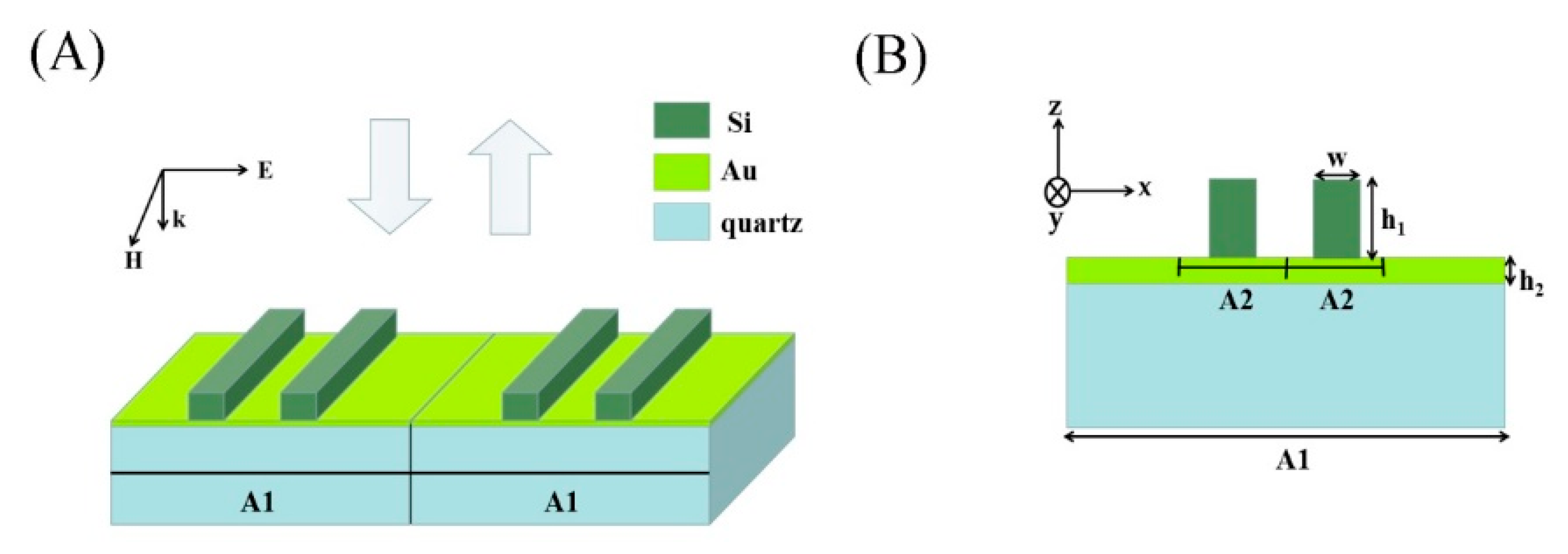
2. Materials and Methods
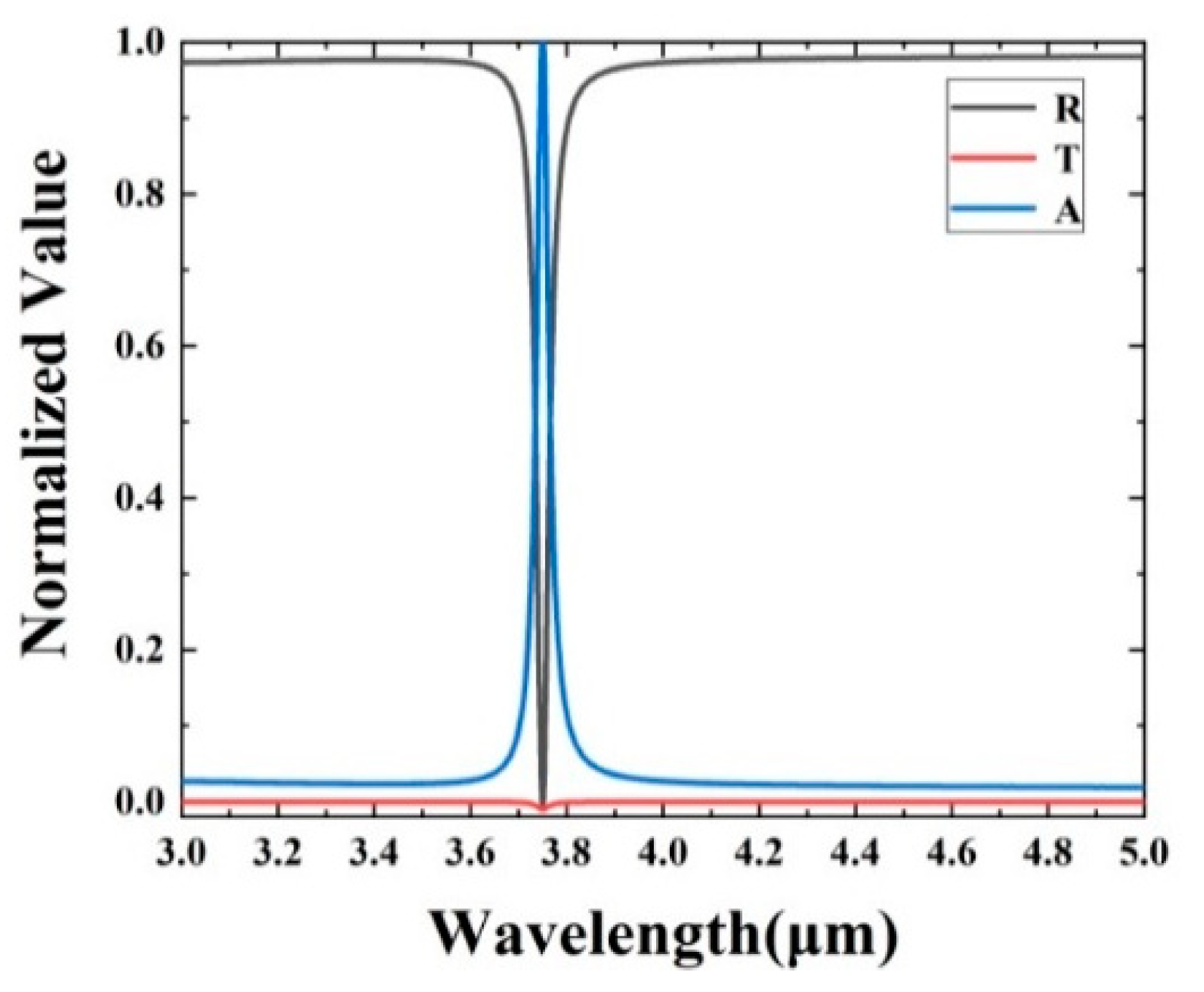
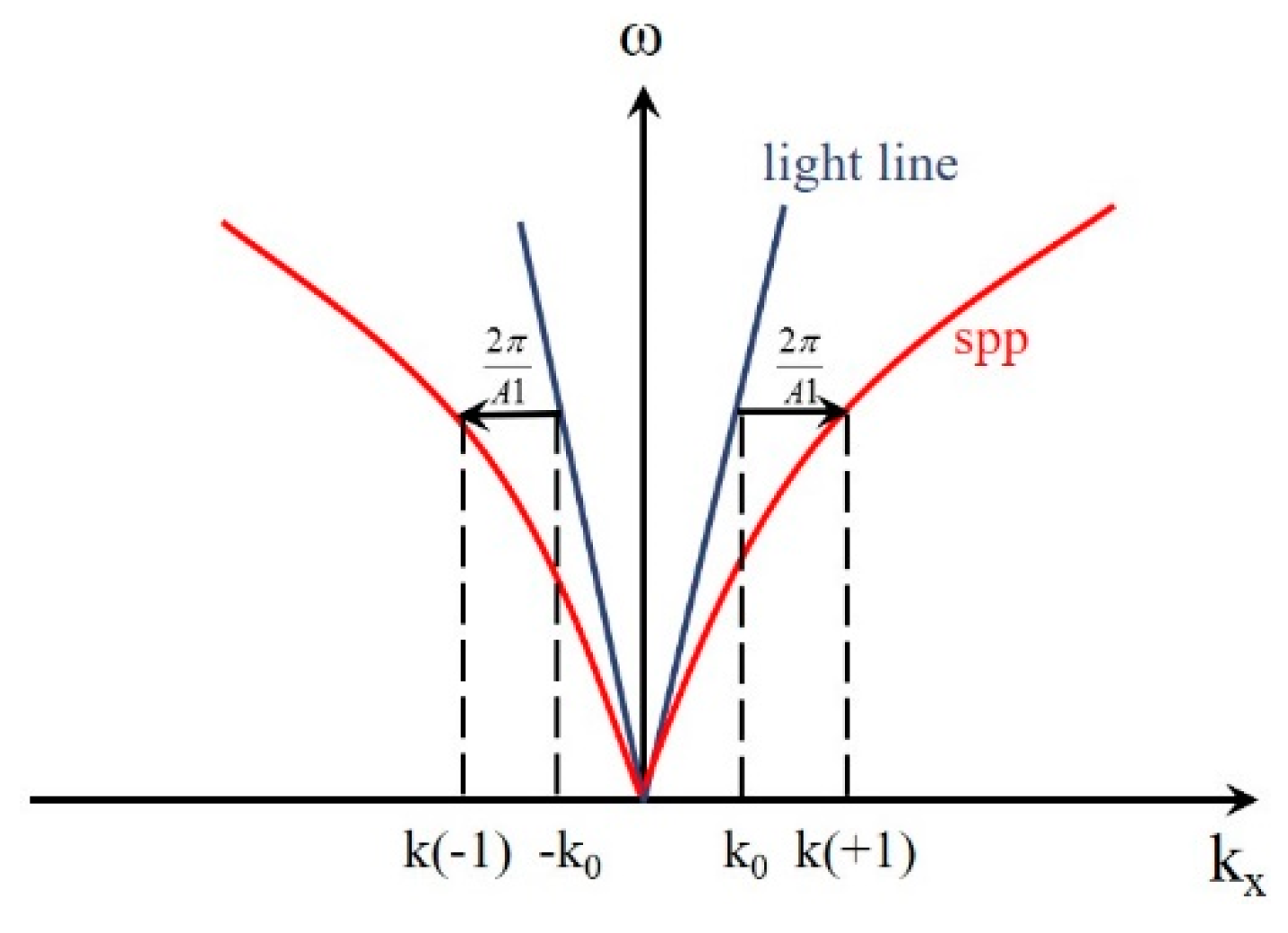
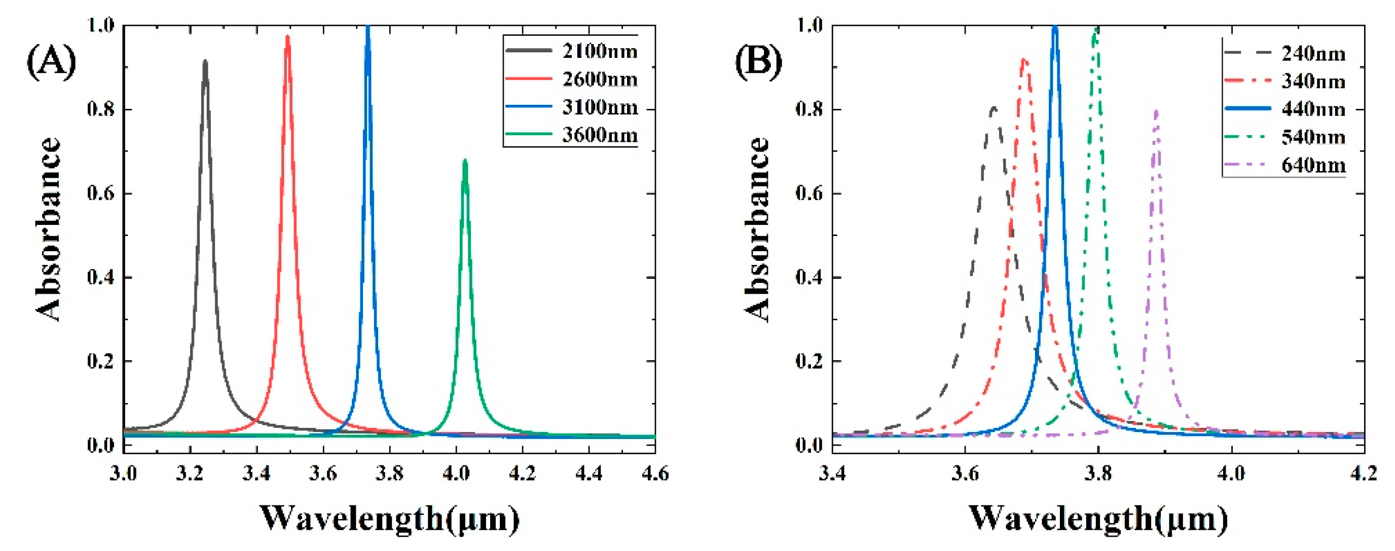
Figure 1A presents the structure of a narrowband perfect absorber of a symmetric Si grating. It is made of a quartz substrate and a Si grid on the surface of the Au thin layer. The optical parameters of Si and Au are obtained from reference [48]. The grating period is A1, and each period has a Si grating structure with two secondary periods (A2); (B) is the section of the single-period grating. h1 is the height of the Si gate. h2 is the thickness of the Au thin layer. w is the thickness of the Si gate. After systematic optimization, the optimal parameters of the absorber are as follows: A1 = 3100 nm, h1 = 630 nm, h2 = 90 nm, w = 260 nm, A2 = 700 nm. For simulating the optical performance of the perfect absorber, we use the FDTD method [49,50,51]. The incident light source is TM (The direction of the electric field is along the X-axis) plane light wave, and the direction of the light source is perpendicular to the grating surface. The X-axis and Y-axis directions are periodic boundary conditions; the Z-axis direction is a perfectly matched layer boundary condition.

3. Results

As shown in Figure 2, in the case of normal incident light waves, we calculate the data of reflectance, transmittance, and absorbance. From Figure 2, we can observe that the transmittance is basically zero, and there is only one reflection inclination within the range of the study spectrum. Then, we use A = 1-R-T to get the reflectance of the structure, and the reflectance of the absorption peak is more than 99%. This reflection peak angle appears at λ = 3750 nm with the full width at half (FWHM) = 30 nm. The structure can be used as an infrared filter.
The symmetric Si grating divides the incident light into many orders. The wave vectors of different orders can be determined by the formula: k(i) = k0sinα + 2πi/A1. In which k0 and k(i) are the wave vectors of incident light and order, i = 0, ±1, ±2... ±n, α is the incident angle. With proper parameters, the order (+1, −1) can connect the plane propagating surface plasmon waves. It can be seen that the coupling resonance between the surface plasmon mode and the incident light leads to strong absorption. Through the wave vector matching condition [52], the coupling process can be expressed as Equations (1) and (2):
2 π n eff ( + 1 ) / λ ( + 1 ) = k ( + 1 ) = k 0 sin   α + 2 π i / A 1
2 π n eff ( 1 ) / λ ( 1 ) = k ( 1 ) = k 0 sin   α     2 π i / A 1
In which neff represents the effective refractive index of the surface plasmon model. λ(+1) and the λ(−1) all mean resonance wavelength. In the case of vertical incidence, α = 0 and λ(+1) = λ(−1), so only one absorption peak occurs. As shown in Figure 3, it is the wave vector matching diagram of the structure.
To better understand the physical mechanism of the symmetrical gratings, electric and magnetic fields are simulated for the peak wavelength [53,54,55]. Figure 4 shows the distribution of the electric field and magnetic field at λ = 3750 nm, respectively. The electric field mainly distributes in the upper inner corner of the horizontal Si grating, and the magnetic field mainly distributes in the groove of the Si grating. This is because of the interaction of light waves with free electrons on the surface, and the motion of the surface plasmon produces surface plasmon waves. Surface plasmon resonance is caused by the coupling between the surface plasmon wave and the electromagnetic field of light. Through the distribution of electric field and magnetic field, we can analyze that a strong rectangular displacement current is formed between the cracks of the Si grating, which is also verified by the distribution of magnetic fields. Both of them meet the right-handed spiral rule.
To systematically study the influence factors of Si grating structure on absorption performance, we use the control variable method to change the geometric parameters of the structure. Figure 5A,B shows the influence of period change and Si grating spacing on the absorption performance of Si grating. Figure 5A shows that the absorption peak wavelength shifts to red, and the absorption peak increases first and then decreases with the change of the Si grating period. Simultaneously, we also notice that the half-height and half-width of the absorption peak gradually decrease with the increase of the period length. This is because the longer the period, the smaller the neff. The influence of the change in the spacing width of the Si grating on the redshift of the peak wavelength is much smaller than that of the period length (In Figure 5B). Similarly, the absorption peak first increases and then decreases with the change of the spacing between the two secondary gratings. The half-height and half-width of the absorption peak decrease with the increase of the Si grating spacing width, which is because the smaller the Si grating spacing is, the stronger the excited electric field is and the greater the displacement current is generated, thus widening the half-height and half-width. In addition, we also note that the absorbance of the absorption peak does not decrease significantly (about 2%) when the Si grating spacing is 540 nm because the Si grating spacing corresponding to the maximum absorbance changed within a certain range, which would not have a great impact on the absorbance.
Figure 6A,B, shows the influence of the Si grating width and the Si grating geometric thickness parameters on the absorption performance of the Si grating. From Figure 6A, we can observe that the absorption peak redshifts as the width of the Si grating increases. Moreover, the redshift distance is larger between the Si grating width of 200 nm and 260 nm. With the redshift of these absorption peaks, the half-height and width of these absorption peaks gradually increase. When the Si grating width is 300 nm, the half-height and width reach the maximum. These absorption peaks also appear to redshift as the thickness of the Si grating increases (As shown in Figure 6B). Although these absorption peaks first increase and then decrease, there was no significant change in the absorption value. We note that at the thickness of the Si grating of 630 nm to 730 nm, the change in the absorption peak is only about 2%. This also indicates that the thickness of the Si grating does not change significantly within a certain height range.
Figure 7 shows the relationship between reflection and polarization angle. Transverse (TM) polarization is 0°. TE polarization is 90°, the electric field is along the Y-axis. The polarization of the incident beam is changed from TM polarization to TE polarization with an interval of 2°. We can see that with the increase of polarization angle, the extinction angle of reflection angle decreases. This means that the absorbance decreases with the increase of polarization angle at λ = 3750 nm. This is because the grating in the wave absorber is a three-dimensional grating with an asymmetric structure. We also note that if the polarization angle is less than 20°, the reflected inclination still has a good extinction effect, indicating that the absorber has a good polarization tolerance [56,57].
The perfect absorber also shows excellent sensing characteristics. Figure 8A shows the absorption peak spectrogram of the Si grating when the refractive index (RI) of the detection environment changes. We observe from the figure that the absorption peak appears to redshift with the increase of the environmental RI. Although the absorbance is decreasing, the absorbance of Si grating still remains 90% or above. However, at the same time, we notice that the half-height and width of the absorption peak remain basically unchanged, and the half-height and width are still around 30 nm. Figure 8B shows the absorption peak wavelength corresponding to the RI with the change of the RI of the surrounding environment. The diagonal data are obtained through our linear fitting. According to the formula, the S and FOM of the grating can be calculated [58,59,60,61]. The slope (K) of the line in Figure 8B is the S of the Si grating, whose value is 2780 nm/RIU. The FWHM of the Si grating structure is 30 nm, FOM = S/FWHM = 92.67. This indicates that the structure has high sensitivity and quasilinear response. The structure can be widely used in optical filtering, spectral sensing, gas detection and other fields.

4. Conclusions

In summary, the main research is symmetrical Si grating, whose basic unit structure is that the base material is nonmetallic oxide Si dioxide, the middle layer is precious metal Au, and the top layer is two symmetrical Si grating. By adjusting the geometrical parameters, we achieve the optimal absorbance of the symmetrical Si grating absorber, that is, a narrow band absorption peak with an absorptivity greater than 99% in the optical band range of 300 nm to 500 nm, and the absorption peak wavelength is λ = 3750 nm. We discuss the optical response mechanism from the principle and the distribution of electromagnetic fields. The main reason why symmetrical Si gratings can interact with light to generate a strong light response is that the Si gratings stimulate the generation of surface plasmon under the action of light, and the motion of the surface plasmon leads to the generation of surface plasmon wave and the coupling between the surface plasmon wave and the incident light results in surface plasmon resonance. In addition, when the period, spacing, thickness and height of symmetrical Si grating change, the absorption peaks all show redshift, among which the periodic change has the greatest influence on the redshift of the absorption peak wavelength. The change of the Si grating spacing has the greatest influence on the absorption peak efficiency and the half-height and width of the absorption peak, indicating that the structure is the most sensitive to the change of the Si grating spacing. Then, we obtain the polarization sensitivity of the symmetrical Si grating structure. With the increase of polarization angle, the extinction angle of reflection angle decreases. When the polarization angle is less than 20°, the reflected dip angle still has a good extinction effect, indicating that the structure has a certain polarization tolerance. In the end, we obtained the sensitivity factor of the RI sensor S = 2780 nm/RIU and the FOM = 92.67. Finally, we designed a structure with high sensitivity and quasilinear response. The structure can be widely used in optical filtering, spectral sensing, gas detection and other fields.

Author Contributions

Conceptualization, M.P., H.H. and W.C.; data curation, W.C., S.L. and Q.X.; formal analysis, F.X. and D.W.; methodology, F.X., D.W., J.F., B.F. and L.C.; resources, L.C.; software, W.C., S.L., Q.X. and D.W.; data curation, M.P.; writing—original draft preparation, M.P.; writing—review and editing, Q.X., F.X., D.W. and L.C. All authors have read and agreed to the published version of the manuscript.

Funding

This work was supported by National Natural Science Foundation of China (21676222, U175252), the Natural Science Foundation of Fujian Province (2018J01559, 2019J01738, 2019J01737, 2019J01732, JT180380, JT180365), Major Program of Natural Science Foundation of Fujian Province for College Young Scholars (No. JZ160456), the PhD Research Startup Foundation of Quanzhou Normal University (G16059), the Quanzhou high level Talents Innovation and Entrepreneurship Project (2018C088R, 2020C004R, 2020C044R, 2018C128R). the Putian University’s scientific research project (2016072).

Institutional Review Board Statement

Not applicable.

Informed Consent Statement

Not applicable.

Data Availability Statement

No new data were created or analyzed in this study. Data sharing is not applicable to this article.

Conflicts of Interest

The authors declare no conflict of interest.

References

  1. Zhang, Y.; Yi, Z.; Wang, X.; Chu, P.; Yao, W.; Zhou, Z.; Cheng, S.; Liu, Z.; Wu, P.; Pan, M.; et al. Dual band visible metamaterial absorbers based on four identical ring patches. Phys. E Low Dimens. Syst. Nanostruct. 2021, 127, 114526. [Google Scholar] [CrossRef]
  2. Jiang, L.Y.; Yuan, C.; Li, Z.Y.; Su, J.; Yi, Z.; Yao, W.T.; Wu, P.H.; Liu, Z.M.; Cheng, S.B.; Pan, M. Multi-band and high-sensitivity perfect absorber based on monolayer grapheme metamaterial. Diam. Relat. Mater. 2021, 111, 108227. [Google Scholar] [CrossRef]
  3. Liu, W.; Pang, L.; Han, H.; Shen, Z.; Lei, M.; Teng, H.; Wei, Z. Dark solitons in WS_2 erbium-doped fiber lasers. Photon. Res. 2016, 4, 111–114. [Google Scholar] [CrossRef]
  4. Gao, E.; Liu, Z.; Li, H.; Xu, H.; Zhang, Z.; Luo, X.; Xiong, C.; Liu, C.; Zhang, B.; Zhou, F. Dynamically tunable dual plas-mon-induced transparency and absorption based on a single-layer patterned graphene metamaterial. Opt. Express 2019, 27, 13884. [Google Scholar] [CrossRef]
  5. Yi, Z.; Li, J.K.; Lin, J.C.; Qin, F.; Chen, X.F.; Yao, W.T.; Liu, Z.M.; Cheng, S.B.; Wu, P.H.; Li, H.L. Broadband polariza-tion-insensitive and wide-angle solar energy absorber based on tungsten ring-disc array. Nanoscale 2020, 12, 23077–23083. [Google Scholar] [CrossRef]
  6. Zhang, X.; Liu, Z.; Zhang, Z.; Gao, E.; Luo, X.; Zhou, F.; Li, H.; Yi, Z. Polarization-sensitive triple plasmon-induced transparency with synchronous and asynchronous switching based on monolayer graphene metamaterials. Opt. Express 2020, 28, 36771–36783. [Google Scholar] [CrossRef]
  7. Li, J.; Chen, X.; Yi, Z.; Yang, H.; Tang, Y.; Yi, Y.; Yao, W.; Wang, J.; Yi, Y. Broadband solar energy absorber based on monolayer molybdenum disulfide using tungsten elliptical arrays. Mater. Today Energy 2020, 16, 100390. [Google Scholar] [CrossRef]
  8. Chu, P.; Chen, J.; Xiong, Z.; Yi, Z. Controllable frequency conversion in the coupled time-modulated cavities with phase delay. Opt. Commun. 2020, 476, 126338. [Google Scholar] [CrossRef]
  9. Yu, P.Q.; Yang, H.; Chen, X.F.; Yi, Z.; Yao, W.T.; Chen, J.F.; Yi, Y.G.; Wu, P.H. Ultra-wideband solar absorber based on re-fractory titanium metal. Renew. Energy 2020, 158, 227–235. [Google Scholar] [CrossRef]
  10. Zhao, F.; Chen, X.; Yi, Z.; Qin, F.; Tang, Y.; Yao, W.; Zhou, Z.; Yi, Y. Study on the solar energy absorption of hybrid solar cells with trapezoid-pyramidal structure based PEDOT:PSS/c-Ge. Sol. Energy 2020, 204, 635–643. [Google Scholar] [CrossRef]
  11. Zhang, Y.; Wu, P.; Zhou, Z.; Chen, X.; Yi, Z.; Zhu, J.; Zhang, T.; Jile, H. Study on Temperature Adjustable Terahertz Metamaterial Absorber Based on Vanadium Dioxide. IEEE Access 2020, 8, 85154–85161. [Google Scholar] [CrossRef]
  12. Qin, F.; Chen, X.; Yi, Z.; Yao, W.; Yang, H.; Tang, Y.; Yi, Y.; Li, H.; Yi, Y. Ultra-broadband and wide-angle perfect solar absorber based on TiN nanodisk and Ti thin film structure. Sol. Energy Mater. Sol. Cells 2020, 211, 110535. [Google Scholar] [CrossRef]
  13. Cen, C.L.; Zhang, Y.B.; Chen, X.F.; Yang, H.; Yi, Z.; Yao, W.T.; Tang, Y.J.; Yi, Y.G.; Wang, J.Q.; Wu, P.H. A dual-band met-amaterial absorber for graphene surface plasmon resonance at terahertz frequency. Physica E 2020, 117, 113840. [Google Scholar] [CrossRef]
  14. Liu, W.; Pang, L.; Han, H.; Bi, K.; Lei, M.; Wei, Z. Tungsten disulphide for ultrashort pulse generation in all-fiber lasers. Nanoscale 2017, 9, 5806–5811. [Google Scholar] [CrossRef] [PubMed]
  15. Liu, W.; Pang, L.; Han, H.; Liu, M.; Lei, M.; Fang, S.; Teng, H.; Wei, Z. Tungsten disulfide saturable absorbers for 67 fs mode-locked erbium-doped fiber lasers. Opt. Express 2017, 25, 2950–2959. [Google Scholar] [CrossRef] [Green Version]
  16. Chen, J.; Nie, H.; Peng, C.; Qi, S.; Tang, C.; Zhang, Y.; Wang, L.; Park, G.-S. Enhancing the Magnetic Plasmon Resonance of Three-Dimensional Optical Metamaterials via Strong Coupling for High-Sensitivity Sensing. J. Light. Technol. 2018, 36, 3481–3485. [Google Scholar] [CrossRef]
  17. Pan, M.; Su, Z.; Yu, Z.; Wu, P.; Jile, H.; Yi, Z.; Chen, Z. A narrowband perfect absorber with high Q-factor and its application in sensing in the visible region. Results Phys. 2020, 19, 103415. [Google Scholar] [CrossRef]
  18. Cen, C.; Chen, Z.; Xu, D.; Jiang, L.; Chen, X.; Yi, Z.; Wu, P.; Li, G.; Yi, Y. High quality factor, high sensitivity metamaterial gra-phene-perfect absorber based on critical coupling theory and impedance matching. Nanomaterials 2020, 10, 95. [Google Scholar] [CrossRef] [Green Version]
  19. He, Z.; Li, L.; Ma, H.; Pu, L.; Xu, H.; Yi, Z.; Cao, X.; Cui, W. Graphene-based metasurface sensing applications in terahertz band. Results Phys. 2021, 21, 103795. [Google Scholar] [CrossRef]
  20. Chen, Z.; Chen, H.; Jile, H.; Xu, D.; Yi, Z.; Lei, Y.; Chen, X.; Zhou, Z.; Cai, S.; Li, G. Mult-band multi-tunable perfect plasmon absorber based on L-shaped and double-elliptical graphene stacks. Diam. Relat. Mater. 2021, 108374. [Google Scholar] [CrossRef]
  21. Liu, N.; Mesch, M.; Weiss, T.; Hentschel, M.; Giessen, H. Infrared Perfect Absorber and Its Application As Plasmonic Sensor. Nano Lett. 2010, 10, 2342–2348. [Google Scholar] [CrossRef]
  22. Wang, X.X.; Zhu, J.K.; Xu, Y.Q.; Qi, Y.P.; Zhang, L.P.; Yang, H.; Yi, Z. A novel plasmonic refractive index sensor based on gold/silicon complementary grating structure. Chin. Phys. B 2021, 30, 024207. [Google Scholar] [CrossRef]
  23. Liu, Q.; Jiang, Y.; Sun, Y.; Hu, C.; Sun, J.; Liu, C.; Lv, J.; Zhao, J.; Yi, Z.; Chu, P.K. Surface plasmon resonance sensor based on U-shaped photonic quasi-crystal fiber. Appl. Opt. 2021, 60, 1761–1766. [Google Scholar] [CrossRef] [PubMed]
  24. Wang, Y.; Yi, Y.; Xu, D.; Yi, Z.; Li, Z.; Chen, X.; Jile, H.; Zhang, J.; Zeng, L.; Li, G. Terahertz tunable three band narrowband perfect absorber based on Dirac semimetal. Phys. E Low Dimens. Syst. Nanostruct. 2021, 131, 114750. [Google Scholar] [CrossRef]
  25. El-Gohary, S.H.; Choi, J.M.; Kim, N.-H.; Byun, K.M. Plasmonic metal–dielectric–metal stack structure with subwavelength metallic gratings for improving sensor sensitivity and signal quality. Appl. Opt. 2014, 53, 2152–2157. [Google Scholar] [CrossRef] [Green Version]
  26. An, S.; Lv, J.; Yi, Z.; Liu, C.; Yang, L.; Wang, F.; Liu, Q.; Su, W.; Li, X.; Sun, T.; et al. Ultra-short and dual-core photonic crystal fiber polarization splitter composed of metal and gallium arsenide. Optik 2021, 226, 165779. [Google Scholar] [CrossRef]
  27. Wu, P.; Wang, Y.; Yi, Z.; Huang, Z.; Xu, Z.; Jiang, P. A Near-Infrared Multi-Band Perfect Absorber Based on 1D Gold Grating Fabry-Perot Structure. IEEE Access 2020, 8, 72742–72748. [Google Scholar] [CrossRef]
  28. Yang, M.M.; Kong, Q.Q.; Feng, W.; Yao, W.T. N/O double-doped biomass hard carbon material realizes fast and stable potas-sium ion storage. Carbon 2021, 176, 71–82. [Google Scholar] [CrossRef]
  29. Wu, P.; Zhang, C.; Tang, Y.; Liu, B.; Lv, L. A Perfect Absorber Based on Similar Fabry-Perot Four-Band in the Visible Range. Nanomaterials 2020, 10, 488. [Google Scholar] [CrossRef] [Green Version]
  30. Qi, Y.; Zhang, B.; Ding, J.; Zhang, T.; Wang, X.; Yi, Z. Efficient Manipulation of Terahertz waves by multi-bit Coding Metasurfaces and its further application. Chin. Phys. B 2020, 30, 024211. [Google Scholar] [CrossRef]
  31. Kuznetsov, A.I.; Miroshnichenko, A.E.; Brongersma, M.L.; Kivshar, Y.S.; Luk’Yanchuk, B. Optically resonant dielectric nanostructures. Science 2016, 354, aag2472. [Google Scholar] [CrossRef] [Green Version]
  32. Sharon, A.; Glasberg, S.; Rosenblatt, D.; Friesem, A.A. Metal-based resonant grating waveguide structures. J. Opt. Soc. Am. A 1997, 14, 588–595. [Google Scholar] [CrossRef]
  33. Cheng, Y.; Fan, J.; Luo, H.; Chen, F. Dual-band and high-effciency circular polarization convertor based on anisotropic metamaterial. IEEE Access 2020, 8, 7615–7621. [Google Scholar] [CrossRef]
  34. Cheng, Z.; Cheng, Y. A multi-functional polarization convertor based on chiral metamaterial for terahertz waves. Opt. Commun. 2019, 435, 178–182. [Google Scholar] [CrossRef]
  35. Cui, Y.; He, Y.; Jin, Y.; Ding, F.; Yang, L.; Ye, Y.; Zhong, S.; Lin, Y.; He, S. Plasmonic and metamaterial structures as electro-magnetic absorbers. Laser Photonics Rev. 2014, 8, 495–520. [Google Scholar] [CrossRef] [Green Version]
  36. Liu, Z.; Zhang, X.; Zhang, Z.; Gao, E.; Zhou, F.; Li, H.; Luo, X. Simultaneous Switching at Multiple frequencies and triple plas-mon-induced transparency in multilayer patterned graphene-based terahertz metamaterial. New J. Phys. 2020, 22, 083006. [Google Scholar] [CrossRef]
  37. Yao, Y.; Liao, Z.; Liu, Z.-Q.; Liu, X.; Zhou, J.; Liu, G.; Yi, Z.; Wang, J. Recent progresses on metamaterials for optical absorption and sensing: A review. J. Phys. D Appl. Phys. 2021, 54, 113002. [Google Scholar] [CrossRef]
  38. Shen, S.; Forsberg, E.; Han, Z.; He, S. Strong resonant coupling of surface plasmon polaritons to radiation modes through a thin metal slab with dielectric gratings. J. Opt. Soc. Am. A 2007, 24, 225–230. [Google Scholar] [CrossRef]
  39. Li, X.; Han, D.; Wu, F.; Xu, C.; Liu, X.; Zi, J. Flat metallic surfaces coated with a dielectric grating: Excitations of surface plasmon–polaritons and guided modes. J. Phys. Condens. Matter 2008, 20, 485001. [Google Scholar] [CrossRef]
  40. Lu, X.; Zhang, T.; Wan, R.; Xu, Y.; Zhao, C.; Guo, S. Numerical investigation of narrowband infrared absorber and sensor based on dielectric-metal metasurface. Opt. Express 2018, 26, 10179–10187. [Google Scholar] [CrossRef]
  41. Fitio, V.M.; Bobitski, Y.V. Resonance effects in a dielectric grating; total absorption of electromagnetic waves by a dielectric grating on metal system. J. Opt. A Pure Appl. Opt. 2004, 6, 943–951. [Google Scholar] [CrossRef]
  42. Liao, Y.-L.; Zhao, Y.; Zhang, X.; Zhang, W.; Chen, Z. An ultra-narrowband TE-polarization absorber with a dielectric grating and metal substrate. Mod. Phys. Lett. B 2017, 31, 1750306. [Google Scholar] [CrossRef]
  43. Yan, P.G.; Chen, H.; Liu, A.J.; Li, K.Y.; Ruan, S.C.; Qiu, X.H.; Guo, T. Self-starting mode-locking by fiber-integrated WS2 sat-urable absorber mirror. IEEE J. Sel. Top. Quantum Electron. 2017, 23, 1100106. [Google Scholar] [CrossRef]
  44. Zhou, W.; Wu, Y.; Yu, M.; Hao, P.; Liu, G.; Li, K. Extraordinary optical absorption based on guided-mode resonance. Opt. Lett. 2013, 38, 5393–5396. [Google Scholar] [CrossRef] [PubMed]
  45. Zhang, S.; Wang, Y.; Zheng, W. Wavelength-tunable perfect absorber based on guided-mode resonances. Appl. Opt. 2016, 55, 3176. [Google Scholar] [CrossRef]
  46. Mohammad, A.; Ibrahim, A. Self-referenced biosensor based on thin dielectric grating combined with thin metal film. Opt. Express 2015, 23, 28667. [Google Scholar]
  47. To, N.; Juodkazis, S.; Nishijima, Y. Detailed Experiment-Theory Comparison of Mid-Infrared Metasurface Perfect Absorbers. Micromachines 2020, 11, 409. [Google Scholar] [CrossRef] [PubMed] [Green Version]
  48. Palik, E.D. Handbook of Optical Constants of Solids; Academic Press: Cambridge, MA, USA, 1998. [Google Scholar]
  49. Chen, H.; Guo, K.; Yin, J.; He, S.; Qiu, G.; Zhang, M.; Xu, Z.; Zhu, G.; Yang, J.; Yan, P. Photoluminescence-Induced Four-Wave Mixing Generation in a Monolayer-MoS 2-Cladded GaN Microdisk Resonator. Laser Photon. Rev. 2021, 2000459. [Google Scholar] [CrossRef]
  50. Wang, J.T.; Jiang, Z.K.; Chen, H.; Wang, J.Z.; He, T.C.; Yan, P.G.; Ruan, S.C. High energy soliton generation by MSD-grown MoTe2 saturable absorber. Photonics Res. 2018, 6, 535–541. [Google Scholar] [CrossRef]
  51. He, Z.; Xue, W.; Cui, W.; Li, C.; Li, Z.; Pu, L.; Feng, J.; Xiao, X.; Wang, X.; Li, A.G. Tunable Fano Resonance and Enhanced Sensing in a Simple Au/TiO2 Hybrid Metasurface. Nanomaterials 2020, 10, 687. [Google Scholar] [CrossRef] [PubMed] [Green Version]
  52. He, X.; Jie, J.; Yang, J.; Chen, Y.; Han, Y.; Zhang, S. Suppressing the unwanted resonance mode in a metal-insulator-metal structure using fine-structured gratings. Opt. Express 2019, 27, 15298–15308. [Google Scholar] [CrossRef]
  53. Zou, H.; Cheng, Y. Design of a six-band terahertz metamaterial absorber for temperature sensing application. Opt. Mater. 2019, 88, 674–679. [Google Scholar] [CrossRef]
  54. Cheng, T.; Gao, H.; Sun, X.; Xian, T.; Wang, S.; Yi, Z.; Liu, G.; Wang, X.; Yang, H. An excellent Z-scheme Ag2MoO4/Bi4Ti3O12 heterojunction photocatalyst: Construction strategy and application in environmental purification. Adv. Powder Technol. 2021, 32, 951–962. [Google Scholar] [CrossRef]
  55. Fan, J.; Cheng, Y. Broadband high-effciency cross-polarization conversion and multi-functional wave front manipulation based on chiral structure metasurface for terahertz wave. J. Phys. D Appl. Phys. 2020, 53, 025109. [Google Scholar] [CrossRef]
  56. Wu, Y.; Wang, X.; Wen, X.; Zhu, J.; Bai, X.; Jia, T.; Yang, H.; Zhang, L.; Qi, Y. Surface-enhanced Raman scattering based on hybrid surface plasmon excited by Au nanodisk and Au film coupling structure. Phys. Lett. A 2020, 384, 126544. [Google Scholar] [CrossRef]
  57. Liu, C.; Wang, J.; Wang, F.; Su, W.; Yang, L.; Lv, J.; Fu, G.; Li, X.; Liu, Q.; Sun, T.; et al. Surface plasmon resonance (SPR) infrared sensor based on D-shape photonic crystal fibers with ITO coatings. Opt. Commun. 2020, 464, 125496. [Google Scholar] [CrossRef]
  58. Wang, Y.; Li, R.; Sun, X.; Xian, T.; Yi, Z.; Yang, H. Photocatalytic Application of Ag-Decorated CuS/BaTiO3 Composite Photocatalysts for Degrading RhB. J. Electron. Mater. 2021, 1–13. [Google Scholar] [CrossRef]
  59. Cheng, T.; Sun, X.; Xian, T.; Yi, Z.; Li, R.; Wang, X.; Yang, H. Tert-butylamine/oleic acid-assisted morphology tailoring of hierarchical Bi4Ti3O12 architectures and their application for photodegradation of simulated dye wastewater. Opt. Mater. 2021, 112, 110781. [Google Scholar] [CrossRef]
  60. Li, J.Y.; Wang, S.F.; Sun, G.G.; Gao, H.J.; Yu, X.L.; Tang, S.N.; Zhao, X.X.; Yi, Z.; Wang, Y.; Wei, Y. Facile preparation of MgAl2O4/CeO2/Mn3O4 heterojunction photocatalyst and enhanced photocatalytic activity. Mater. Today Chem. 2021, 19, 100390. [Google Scholar] [CrossRef]
  61. Liu, C.; Wang, J.; Jin, X.; Wang, F.; Yang, L.; Lv, J.; Fu, G.; Li, X.; Liu, Q.; Sun, T.; et al. Near-infrared surface plasmon resonance sensor based on photonic crystal fiber with big open rings. Optik 2020, 207, 164466. [Google Scholar] [CrossRef]
Figure 1. (A) Three-dimensional diagram of symmetrical Si grating structure and (B) section diagram of element structure.
Coatings 11 00553 g001
Figure 2. Spectrogram of reflectance (R), transmittance (T), and absorbance (A) under the normal incidence of symmetrical Si grating.
Coatings 11 00553 g002
Figure 3. Wave vector matching graph.
Coatings 11 00553 g003
Figure 4. The distribution of electric field (A) and magnetic field (B) on the XOZ section at λ = 3750 nm of the symmetric Si grating. The grating is outlined with white lines.
Coatings 11 00553 g004
Figure 5. Periodic parameters of symmetrical Si grating (A) and spacing parameters of the two secondary gratings (B).
Coatings 11 00553 g005
Figure 6. Parameters of the width of symmetrical Si grating (A) and thickness of symmetrical Si grating (B).
Coatings 11 00553 g006
Figure 7. Relation diagram of reflectance and polarization angle of Si grating.
Coatings 11 00553 g007
Figure 8. (A) Absorbance spectrogram and (B) relationship between RI and the corresponding peak wavelength of symmetrical Si grating under RI change. K and S represent the slope of the straight line and the sensitivity of the structure, respectively.
Coatings 11 00553 g008
Publisher’s Note: MDPI stays neutral with regard to jurisdictional claims in published maps and institutional affiliations.

