
Magnetotransport Properties of Semi-Metallic Bismuth Thin Films for Flexible Sensor Applications


Department of Magnetic Materials and Nanostructures, Institute of Nuclear Physics Polish Academy of Sciences, PL-31342 Krakow, Poland
*
Author to whom correspondence should be addressed.
Coatings 2021, 11(2), 175; https://doi.org/10.3390/coatings11020175
Submission received: 11 January 2021
/
Revised: 24 January 2021
/
Accepted: 27 January 2021
/
Published: 2 February 2021
(This article belongs to the Special Issue Advances in Flexible Films and Coatings)
Abstract
:In this paper we describe characterization of semi-metallic bismuth thin films. We prepared bismuth thin films by a deposition of bismuth through thermal evaporation onto flexible Kapton substrates and annealing at temperatures close to the melting point of Bi. We studied the morphology and transport properties of these films. Immediately after the deposition we observed competition between vanishing of the grain boundaries and elastic strain energy, which stabilized at larger thicknesses leading to the grain size of 140 nm. This effect was accompanied by a continuous decrease of resistivity which, however, was larger than for the bulk bismuth. The film annealing at temperatures close to the melting point of Bi led to a 300% increase of magnetoresistance at room temperature and in the magnetic field of 7 T. The in situ resistance measurements allowed us to determine the permissible temperature at which the annealing does not cause the loss of film continuity.
1. Introduction
The elements in the conventional thin film electronics are composed of active layers deposited on the inflexible substrates and supported by rigid printed circuit boards. In the last decade, however, we have seen a tremendous progress in the area of soft electronics. For soft electronics all components are fabricated on the flexible substrates that can be wrapped, folded, twisted, or bent [1,2,3,4]. This allows to adjust the shape of the resultant devices and to use them in a demanding environment, i.e., where space is limited in size or curved. Examples of soft electronics applications include organic photovoltaics [5], light emitting diodes [6], thin film transistors [7], batteries [8], sensors and actuators [9], and wearable devices [10]. The fields of large area electronics such as panel displays [11], medical imaging equipment [12], or bendable smartphones [13], are also growing fast.
Flexible sensors, such as magnetic fields or strain sensors, play an extremely important role in these applications because most of modern electronic devices need a set of sensors to function properly. However, despite the rapid development of flexible electronics, some problems still remain unresolved in the area of sensors. One of them is the choice of a material for the active thin film element that would be able to show high performance and required functionalities (e.g., magnetoresistance) when bending, stretching and folding. At the same time, it needs to be cheap, robust, and easy to manufacture. One of the materials that has attracted a lot of attention in this context is bismuth. It shows distinctive electronic properties such as low carrier density, small carrier effective mass, high carrier mobility, and a long carrier mean free path [14,15,16]. Thin layers and nanostructures of bismuth offer also a very high magnetoresistance, reaching even 380,000% at low temperatures [17]. These properties make bismuth a good candidate for the use in sensors, and the literature devoted to the fabrication of low dimensional Bi structures and their magnetotransport properties is expanding fast [18,19,20,21,22]. Bi films can be fabricated by various techniques such as liquid-based exfoliation [23,24], molecular beam epitaxy [25], and acid intercalated exfoliation [26].
However, many properties of these films such as morphology, details of crystal structure, and electrical properties are so far not well known. Practical application of Bi film films requires controlled synthesis of the large scale and high-quality layers. Additionally, most of the published reports deal with Bi layers deposited on rigid substrates, such as silicon or Al2O3. To use this material in flexible devices it is necessary to understand how its structure and electrical properties behave after deposition on a flexible polymer substrate. For this purpose, we investigated the properties of a thin Bi layer with various thicknesses from 50 nm up to 2 µm deposited on a flexible Kapton foil. We determined the structure and morphology of the layers and correlated them with magnetotransport properties such as magnetoresistance and the Hall effect. Finally, we showed how the properties of the layers can be improved by controlled post-annealing performed under vacuum conditions.
2. Materials and Methods
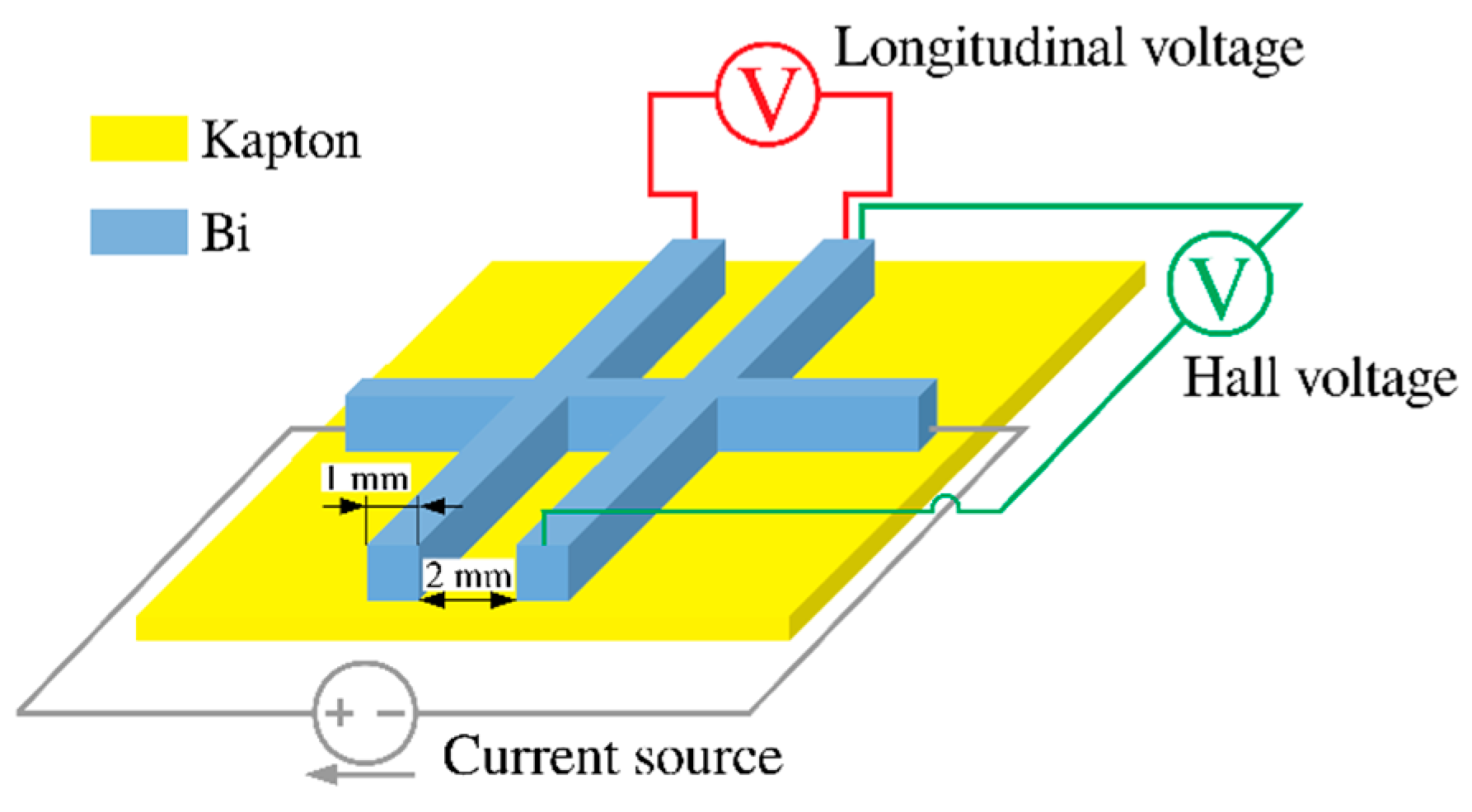
Bismuth (purity 99.999%) was deposited by thermal evaporation in a vacuum of 10−6 mbar on the polyimide foil (Kapton) 12.7 µm thick. The Bi film thickness, controlled during evaporation by quartz monitors with an accuracy of 2%–5%, ranged from 10 nm to 3 µm. For deposition we used double-cross stencil mask to fabricate the film shape suitable for the four-point magnetoresistance measurements done simultaneously with the Hall effect measurements. The configuration of the measurements is schematically shown in Figure 1. In this experiment the sample was placed either in the magnetic field of an electromagnet (magnetic field range from 0 to 2 T, 300 K) or in a magnetic field of Quantum Design MPMS XL system (magnetic field range from 0 to 7 T, temperature range from 4 K to 300 K, Quantum Design, San Diego, CA, USA). In both cases the magnetic field was perpendicular to the sample plane.
We used the current of 1 mA applied in the longitudinal direction while the transversal contacts were used for the voltage and Hall voltage measurements. The width of contacts was 1 mm, and the distance between them was 2 mm. The surface morphology of the films was examined using a scanning electron microscope (SEM, Tescan Vega 3, TESCAN, Brno-Kohoutovice, Czechia), and the X-ray diffraction (XRD) measurements were done with the Panalytical X’Pert Pro instrument (Malvern Panalytical, Almelo, The Netherlands).
3. Results and Discussion
3.1. Structure and Transport Properties of As-Grown Bi Films
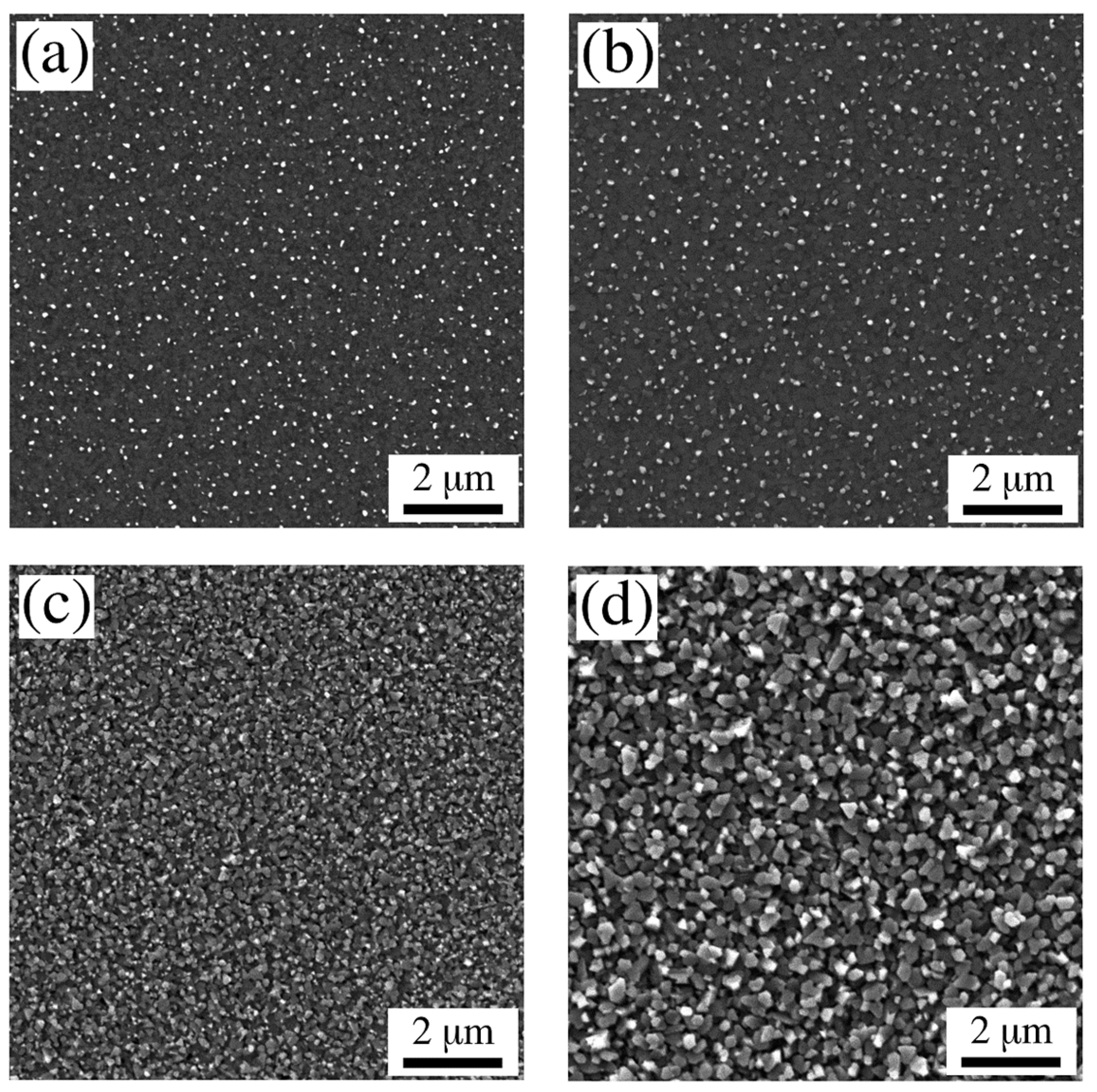
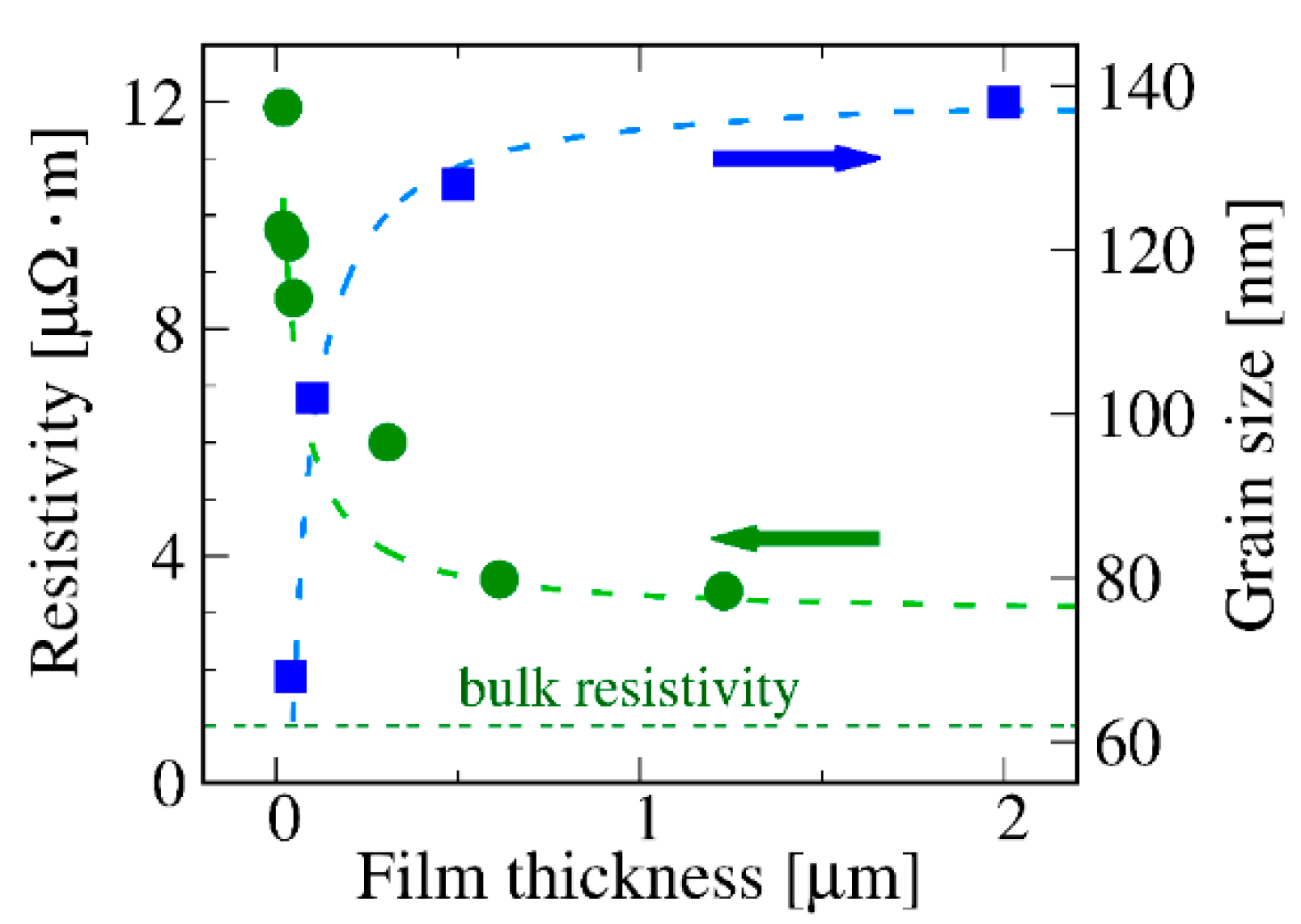
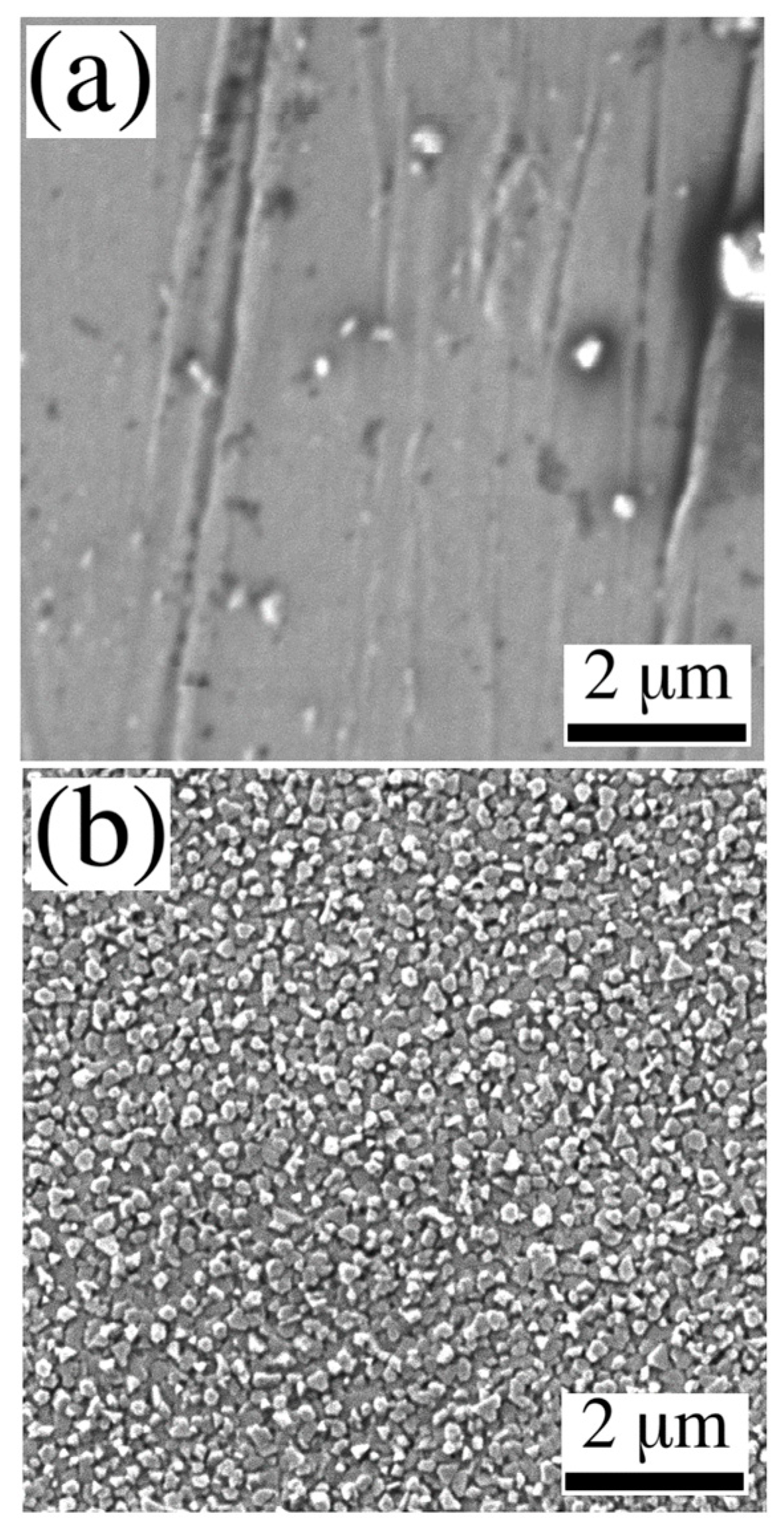
The surface morphology of these Bi films was studied by SEM. Selected scans for film thickness between 40 nm and 2 µm are shown in Figure 2, which shows that the grain size increases with the increase of the thickness. The grain size was determined using an intercept method. A random straight line through a micrograph was drawn and the number of grain boundaries intersecting the line was counted. The average grain size was calculated by dividing the number of intersections by the line length. This was repeated a few tens of times for each image, and next the distribution of grain size was fitted with a Gauss function. The full width at half maximum (FWHM) of the Gauss distribution determined the average grain size which is shown in Figure 3. For film thickness below 0.5 µm the grains are small and their size increases with the thickness increase; above this thickness the grain size stabilizes at the level of approximately 140 nm.
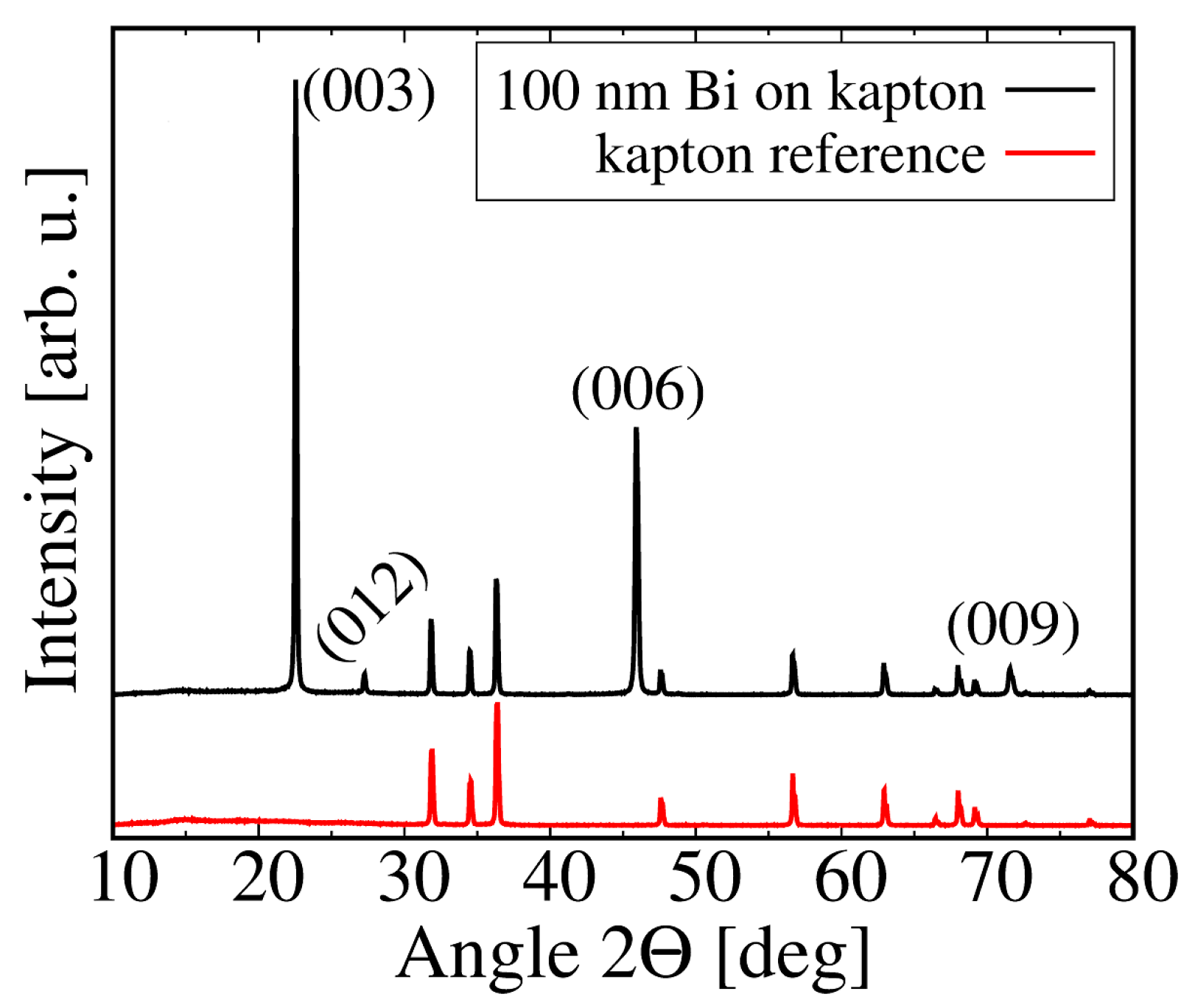
The samples showed a polycrystalline structure indicated in Figure 4 which demonstrates a diffractogram of 100 nm Bi film deposited on Kapton together with Kapton reference. The indexed diffraction peaks match very well the rhombohedral crystal structure of bismuth according to database ICDD PDF file 85-1329.
It is well known [27] that the growth of polycrystalline films generally begins with the thermally activated nucleation of islands or clusters on the surface, followed by a successive island coalescence and the final creation of a continuous film. During the growth of polycrystalline films the Ostwald ripening usually occurs. It is an effect of the growth of the larger islands at the expense of smaller islands, which leads to the increase of the grain size for sufficiently thick films. During the growth the compressive stress that appears early in the deposition process is usually attributed to the presence of the surface and/or interface stress. Upon further growth, the internal elastic strain in the crystallites starts to relax when the growing islands begin to form a continuous layer. At this point the compressive stress converts to tensile stress related to the creation of the grain boundaries elastically accommodated in the lattice. Then, the density of grain boundaries decreases, leading to the reappearance of the compressive stress. The competition between vanishing of grain boundaries and elastic strain energy leads to the stabilization of the compressive stress and in effect also the value of grain size, as observed in Figure 3. This mechanism partially explains resistivity dependence on thickness; a smaller density of grain boundaries is equivalent to a smaller number of electrons scattering centers.
For the thickness below 50 nm we observed a sharp drop of resistivity with the maximum at 20 nm corresponding to the percolation threshold. Above the thickness of 50 nm resistivity drops down and becomes thickness-independent at approximately 0.5 µm with the value three-fold exceeding the bulk value of Bi [26]. The carrier transport is related to two factors: scattering of carriers on both external interfaces (film-substrate, and film-vacuum) and scattering inside the film on the defect and grain boundaries. For thicker films the contribution of the latter factor is dominant, limiting the carrier mobility which results in a resistivity value larger than for bulk. In this case the initial drop of resistivity (for film thickness between the maximum resistivity and 0.5 µm) is related to a small free path of carriers due to scattering on interfaces and defects, while above this Bi thickness the main mechanism limiting the mean free path of carriers and not allowing to reach resistivity bulk values is the presence of the defect and grain boundaries. The value of resistivity for thicker films is approximately 4 µΩ·m, and is close to that obtained by other researchers [28,29] for polycrystalline Bi films deposited on rigid substrates.
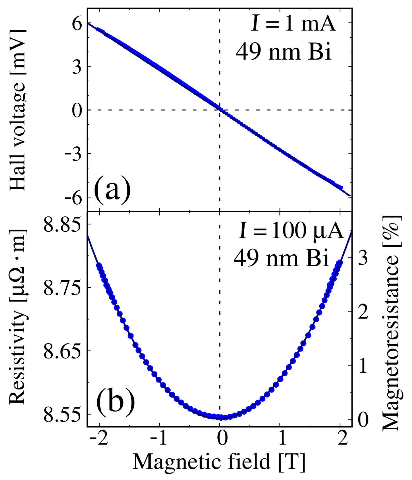
Examples of the magnetoresistance and Hall voltage, measured for Bi film of thickness of 49 nm, are shown in Figure 5. Because the Hall voltage VH can be described as , where RH is the Hall constant, h—film thickness, B—magnetic induction and I—current, it should exhibit a linear dependence on B, while for magnetoresistance one can expect the parabolic dependence on B. Both curves show such dependences on the magnetic field. The negative slope of the Hall voltage magnetic field dependence indicates the n-type character of conductivity as observed also for this range of Bi thickness in other studies [27,28,29].
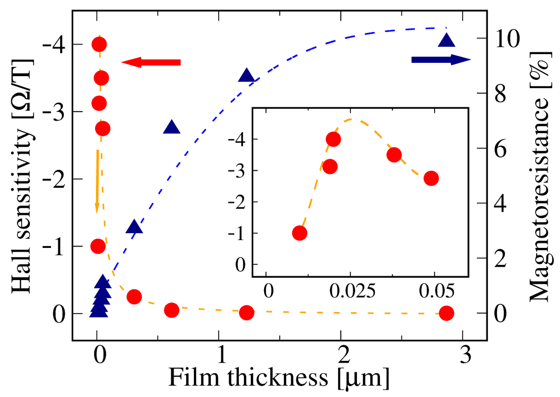
The dependence of magnetoresistance changes and Hall sensitivity on Bi thickness, measured for the magnetic field of 1 T, is demonstrated in Figure 6, while the inset shows the Hall sensitivity for the range of small thicknesses. The observed dependence could be related to the quantum size effects observed in Bi [30]. The value of the Hall coefficient obtained from fitting of the Hall sensitivity with the formula is 0.08 cm3/C and agrees well with known data from other studies [31]. The continuous increase of magnetoresistance with thickness plateaus for the Bi thickness of approximately 2 µm at the level of 10%. This is related to the fact that for larger film thickness the scattering of carriers at interfaces is negligible. The main contribution to the carriers scattering, whose origins are grain boundaries, does not change for the Bi thickness larger than 1 µm, as demonstrated in Figure 3, leading to a constant value of magnetoresistivity. This type of thickness dependence was already observed both for polycrystalline and for single crystal Bi films [17]. On the other hand, the Hall sensitivity reaches the highest value at Bi thickness of approximately 20 nm and then drops down with the Bi thickness. For the Hall measurement the interface substrate-film and its quality are more significant. This can be understood when looking at SEM images for thin (10 nm) and thick (600 nm) films shown in Figure 7. For the thin film one can see numerous defects related to the roughness of the Kapton substrate which was approximately 10 nm, as estimated from atomic force microscopy (AFM) images. For larger thicknesses the film uniformly covers the substrate and the influence of substrate imperfections is not substantial anymore; Hall sensitivity remains constant.
3.2. Magnetotransport Enhancement by Annealing
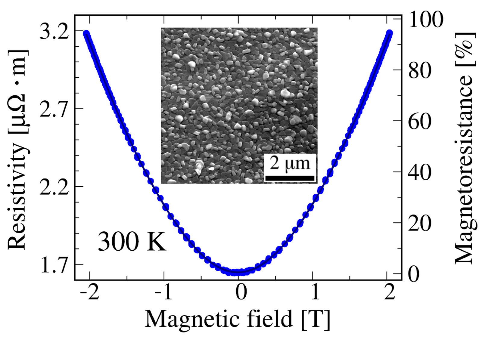
Two main factors governing the conductivity of Bi films are carrier density and their mobility. It is known that the Fermi surface of Bi is highly anisotropic and has small hole pockets and electron pockets occupying only a tiny fraction of the volume of the Brillouin zone. This results in a very low carrier density (~1023 m−3), which means that the probability of carrier scattering and of extremely long mean free path of the range of mm at cryogenic temperatures is low. This feature cannot be intentionally changed in an experiment, contrary to carrier mobility that is limited by the presence of defects in as-grown films. The reduction of defect population by post-deposition film annealing and deposition of films on heated substrates were shown in [10] to be an effective way to increase resistivity. The maximum magnetoresistivity values were obtained for annealing at temperatures close to the melting point of Bi (271.4 °C) which is favorable for recrystallization processes and for the lattice defects reduction. In Figure 8 we present examples of the room temperature measurement of magnetoresistance of 1 µm thick Bi film annealed 80 h at temperature of 240 °C; we also show a SEM image of the film surface.
In comparison to the as-grown sample (Figure 3), the resistivity at a zero magnetic field decreased after annealing more than two times, and the magnetoresistance value at the magnetic field of 1 T is 2.5 times larger than for as-grown samples. This indicates a decrease of defect concentration and grain size increase which is equivalent to a decrease of grain boundary densities being the main reason for carriers scattering. The comparison of these results with others obtained for polycrystalline Bi films deposited with different techniques [17,32] shows that despite a non-typical substrate (Kapton) with large roughness we managed to obtain a reasonable improvement of the magnetoresistance. The improvement can be even more pronounced for the experiments performed at lower temperatures or higher magnetic fields, which is demonstrated in Figure 9.
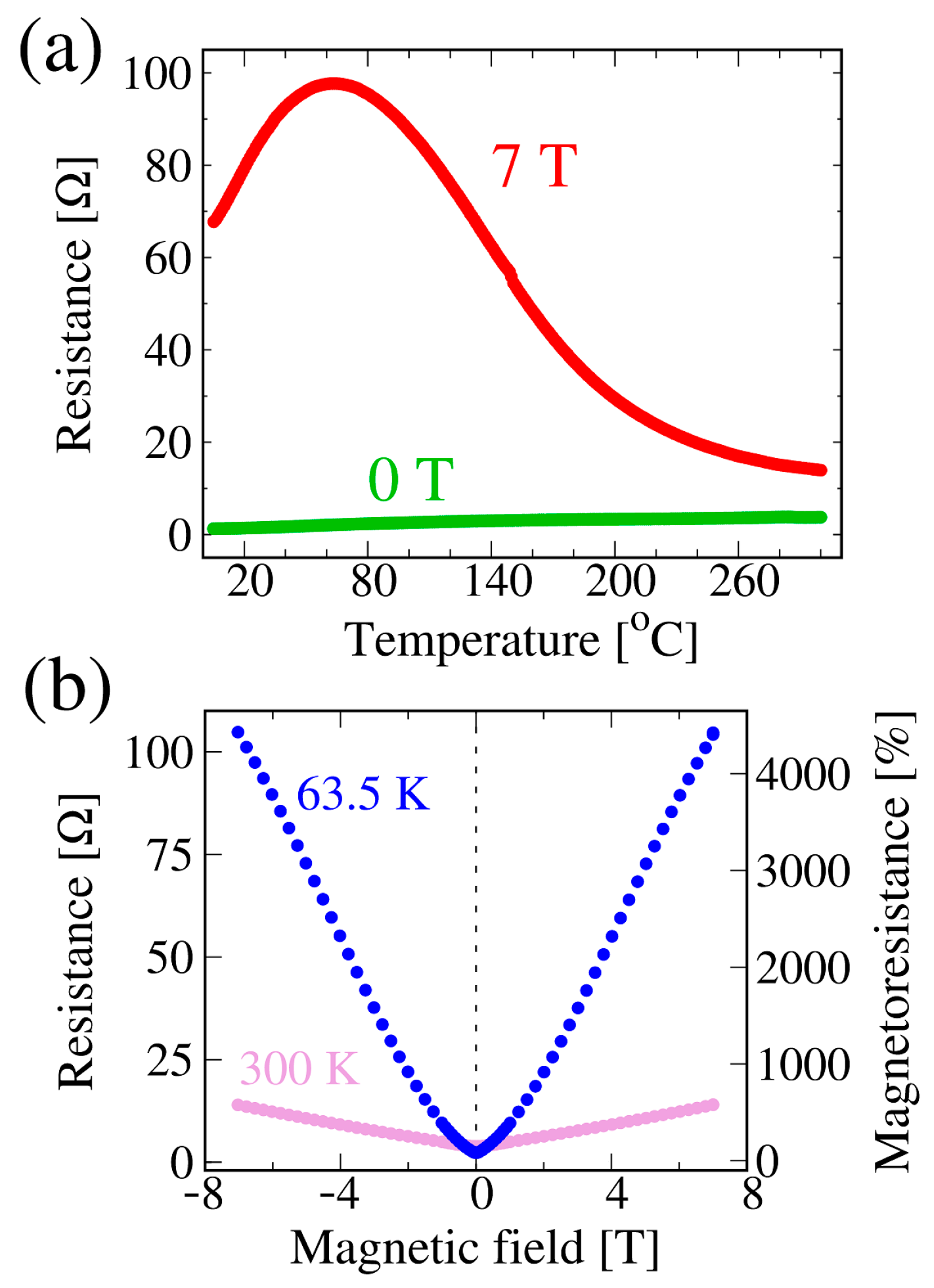
The temperature dependent resistance measured at the magnetic field of 7 T drastically raises with decreased temperature, reaching a maximum at 63.5 K. This corresponds to the maximum of the carrier mobilities. The magnetoresistance change measured for this temperature in the magnetic field range from 0 to 7 T was equal to 4000% in comparison to the room temperature value of 300%. Numerous experiments at low temperatures demonstrate huge values of magnetoresistance of the order of thousands of percent; however, they are usually performed for single crystalline Bi films obtained by expensive and time consuming techniques such as molecular beam epitaxy. The largest magnetoresistance values for polycrystalline films deposited on rigid substrates, such as silicon or glass, are smaller [17,30] and at room temperature do not exceed the value of several percent, smaller than obtained in our experiment.
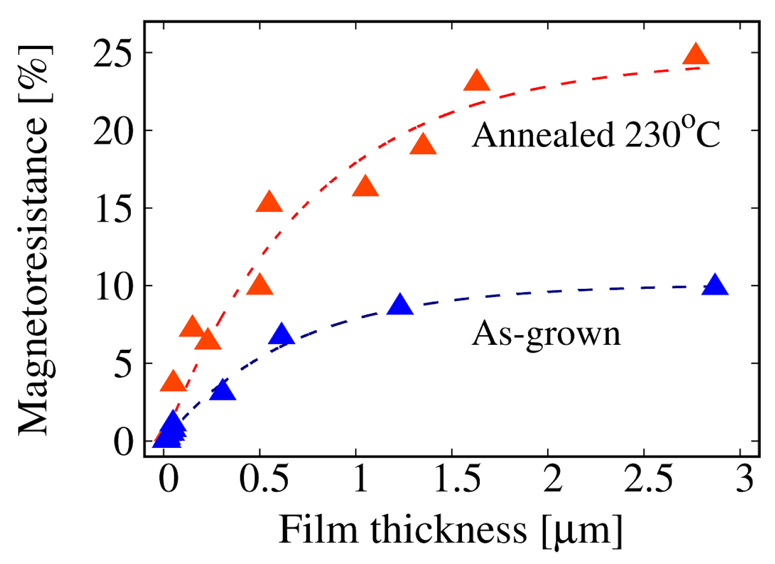
The summary of post annealing influence on magnetoresistance value is shown in Figure 10 for Bi film annealed at 230 °C. The annealing temperature was chosen close to the melting point of Bi but low enough not to destroy the continuity of thinner films. The annealing leads to material recrystallization, defect recombination and grain boundary reduction which elongate the mean free path of charge carriers and decrease resistance. According to Matthiessen’s rule, if initial resistivity is substantially decreased, it is accompanied by a significant increase in magnetoresistivity. To observe processes taking part during annealing of Bi films we performed in situ measurement of resistivity (Figure 11).
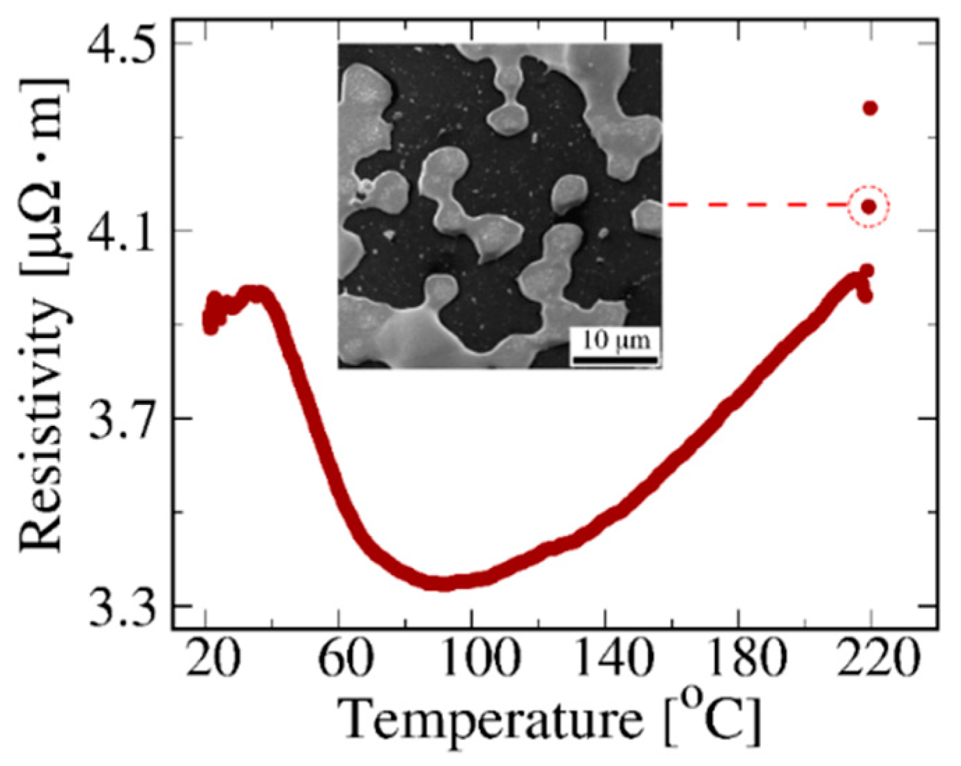
At lower temperatures the resistivity significantly decreases because of the defect removal. At 90 °C the resistivity starts to increase and from 150 °C this dependence follows linear approximation, as known for metallic conductivity, up to temperatures close to the Bi melting point. At this point the sharp change of resistivity is observed, assigned to loss of film continuity (as shown in the inset of Figure 11). The system goes beyond the percolation threshold and ceases to be conductive. The region marked with a red circle with a small drop of resistivity corresponds to the transition between solid and liquid Bi metal observed also for bulk materials [33]. These measurements allow us to determine maximum critical temperature at which the film still preserves continuity and the dewetting process is not initiated. The critical temperature used for annealing strongly depends on film thickness because of thickness dependent contributions of surface energy and the mechanical strain to thermodynamics of the recrystallization process. These factors, in turn, influence the annealing time which can change from a few hours for higher temperatures to a few tens of hours if a lower annealing temperature is necessary. In this process we observed two competing mechanisms: annealing of defects and the standard dependence R(T) for metals completed by the local melting of film and its dewetting. We performed similar measurements for other Bi thicknesses, and observed that the critical temperature at which the film was losing the continuity decreased with film thickness and grain size. This is also observed for thin films of low melting elements [34]. Overall, we conclude that the annealing conditions have to be tuned separately for each thickness of Bi film in order to enhance the magnetoresistance value.
4. Conclusions
We studied the surface morphology and magnetotransport properties of the Bi films deposited on polymer flexible substrate. These substrates are essential for future applications in shapeable electronics. For as-grown Bi films we observed a decrease of resistance for increasing film thickness related to the presence of extrinsic and intrinsic effects. For lower Bi thicknesses both effects play an equally important role in carrier scattering, while for larger thicknesses the impact of grain boundaries becomes dominant. However, even for the thickest Bi films the resistivity value was more than two times larger than in the case of the bulk material. This resulted in small values of magnetoresistance change. The annealing of samples significantly improved the magnetotransport properties. We demonstrated that magnetoresistance increased approximately three times in the annealed samples. The annealing conditions have to be optimized separately for each thickness due to the different amount of grain boundaries and other defects present in films. The resistance of Bi film measured during annealing showed first a decrease with temperature related to defect annealing, then a linear temperature dependence that is usual for metals, and finally a sharp drop due to film dewetting. For temperature dependence of resistance we also observed the transition from solid to liquid metallic phase known for bulk metallic bismuth. The temperature and magnetic field dependent resistance exhibited the magnetoresistance change as large as 4000% demonstrating good capabilities of Bi deposited on Kapton for future applications. The significantly enhanced magnetoresistance of Bi layers can be used to design the magnetic field sensor operated at the range of cryogenic temperatures and at high magnetic fields.
Author Contributions
Conceptualization, Y.Z. and M.M.; methodology, Y.Z. and M.M.; investigation, Y.Z., M.P., A.Z., and M.K.; data analysis, Y.Z.; writing—original draft preparation, Y.Z. and M.M.; writing—review and editing, M.M. and M.K.; supervision, M.M.; project administration, Y.Z.; funding acquisition, Y.Z. All authors have read and agreed to the published version of the manuscript.
Funding
This research was funded by the National Centre for Research and Development within the LIDER V program, Poland (project Nr.: LIDER/008/177/L-5/13/NCBR/2014).
Data Availability Statement
The datasets generated and analysed during the current study are available from the corresponding author on reasonable request.
Conflicts of Interest
The authors declare no conflict of interest. The funders had no role in the design of the study; in the collection, analyses, or interpretation of data; in the writing of the manuscript, or in the decision to publish the results.
References
- Makarov, D.; Melzer, M.; Karnaushenko, D.; Schmidt, O.G. Shapeable magnetoelectronics. Appl. Phys. Rev. 2016, 3, 011101. [Google Scholar] [CrossRef] [Green Version]
- Kim, M.; Oh, S.; Jeong, W.; Talantsev, A.; Jeon, T.; Chaturvedi, R.; Lee, S.; Kim, C. Bendable planar hall resistance sensor. IEEE Magn. Lett. 2020, 11, 1–5. [Google Scholar] [CrossRef]
- Lin, J.; Zhu, Z.; Cheung, C.F.; Yan, F.; Li, G. Digital manufacturing of functional materials for wearable electronics. J. Mater. Chem. C 2020, 8, 10587–10603. [Google Scholar] [CrossRef]
- Karnaushenko, D.; Kang, T.; Schmidt, O.G. Shapeable material technologies for 3D self-assembly of mesoscale electronics. Adv. Mater. Technol. 2019, 4, 1800692. [Google Scholar]
- Kaltenbrunner, M.; White, M.S.; Głowacki, E.D.; Sekitani, T.; Someya, T.; Serdar Sariciftci, N.; Bauer, S. Ultrathin and lightweight organic solar cells with high flexibility. Nat. Commun. 2012, 3, 770. [Google Scholar] [CrossRef] [Green Version]
- Han, T.-H.; Lee, Y.; Choi, M.-R.; Woo, S.-H.; Bae, S.-H.; Hong, B.H.; Ahn, J.-H.; Lee, T.-W. Extremely efficient flexible organic light-emitting diodes with modified graphene anode. Nat. Photonics 2012, 6, 105–110. [Google Scholar] [CrossRef]
- Nomura, K.; Takagi, A.; Kamiya, T.; Ohta, H.; Hirano, M.; Hosono, H. Amorphous oxide semiconductors for high-performance flexible thin-film transistors. Jpn. J. Appl. Phys. 2006, 45, 4303–4308. [Google Scholar] [CrossRef]
- Hu, L.; Wu, H.; La Mantia, F.; Yang, Y.; Cui, Y. Thin, flexible secondary li-ion paper batteries. ACS Nano 2010, 4, 5843–5848. [Google Scholar] [CrossRef]
- Yeo, J.C.; Yap, H.K.; Xi, W.; Wang, Z.; Yeow, C.-H.; Lim, C.T. Flexible and stretchable strain sensing actuator for wearable soft robotic applications. Adv. Mater. Technol. 2016, 1, 1600018. [Google Scholar] [CrossRef]
- Melzer, M.; Ingolf Mönch, J.; Makarov, D.; Zabila, Y.; Santiago Cañón Bermúdez, G.; Karnaushenko, D.; Baunack, S.; Bahr, F.; Yan, C.; Kaltenbrunner, M.; et al. Wearable magnetic field sensors for flexible electronics. Adv. Mater. 2015, 27, 1274–1280. [Google Scholar] [CrossRef]
- Phillips, W.G.; Jano, B. System and Method for Bendable Display. U.S. Patent US9117384B2, 25 August 2015. [Google Scholar]
- Park, S.; Ahn, S.; Sun, J.; Bhatia, D.; Choi, D.; Seung Yang, K.; Bae, J.; Park, J.-J. Highly bendable and rotational textile structure with prestrained conductive sewing pattern for human joint monitoring. Adv. Funct. Mat. 2019, 29, 1808369. [Google Scholar] [CrossRef]
- Burstyn, J.; Banerjee, A.; Vertegaal, R. FlexView: An evaluation of depth navigation on deformable mobile devices. In TEI’13, 7th International Conference on Tangible, Embedded and Embodied Interaction; ACM: New York, NY, USA, 2013; pp. 193–200. [Google Scholar]
- Li, L.; Checkelsky, J.G.; Hor, Y.S.; Uher, C.; Hebard, A.F.; Cava, R.J.; Ong, N.P. Phase transitions of Dirac electrons in bismuth. Science 2008, 321, 547–550. [Google Scholar] [CrossRef] [PubMed] [Green Version]
- Behnia, K.; Balicas, L.; Kopelevich, Y. Signatures of electron fractionalization in ultraquantum bismuth. Science 2007, 317, 1729–1731. [Google Scholar] [CrossRef] [Green Version]
- Zhu, Z.; Collaudin, A.; Fauqué, B.; Kang, W.; Behnia, K. Field-induced polarization of Dirac valleys in bismuth. Nat. Phys. 2012, 8, 89–94. [Google Scholar] [CrossRef]
- Yang, F.Y.; Liu, K.; Hong, K.; Reich, D.H.; Searson, P.C.; Chien, C.L. Large magnetoresistance of electrodeposited single-crystal bismuth thin films. Science 1999, 284, 1335–1337. [Google Scholar] [CrossRef] [Green Version]
- Krupinski, M.; Zarzycki, A.; Zabila, Y.; Marszałek, M. Weak antilocalization tailor-made by system topography in large scale bismuth antidot arrays. Materials 2020, 13, 3246. [Google Scholar] [CrossRef] [PubMed]
- Zabila, Y.; Horeglad, P.; Krupinski, M.; Zarzycki, A.; Perzanowski, M.; Maximenko, A.; Marszałek, M. Optical diffraction strain sensor prepared by interference lithography. Acta Phys. Pol. A 2018, 133, 309–312. [Google Scholar] [CrossRef]
- Melzer, M.; Makarov, D.; Schmidt, O.G. A review on stretchable magnetic field sensorics. J. Phys. D Appl. Phys. 2020, 53, 083002. [Google Scholar] [CrossRef]
- Granell, P.N.; Wang, G.; Cañon Bermudez, G.S.; Kosub, T.; Golmar, F.; Steren, L.; Fassbender, J.; Makarov, D. Highly compliant planar Hall effect sensor with sub 200 nT sensitivity. NPJ Flex. Electron. 2019, 3, 1–6. [Google Scholar] [CrossRef] [Green Version]
- Walker, E.S.; Na, S.R.; Jung, D.; March, S.D.; Kim, J.-S.; Trivedi, T.; Li, W.; Tao, L.; Lee, M.L.; Liechti, K.M.; et al. Large-area dry transfer of single-crystalline epitaxial bismuth thin films. Nano Lett. 2016, 16, 6931–6938. [Google Scholar] [CrossRef]
- Zhao, H.; Sun, X.; Zhu, Z.; Zhong, W.; Song, D.; Lu, W.; Tao, L. Physical vapor deposited 2D bismuth for CMOS technology. J. Semicond. 2020, 41, 081001. [Google Scholar] [CrossRef]
- Yang, B.; Li, X.; Cheng, Y.; Duan, S.; Zhao, B.; Yi, W.; Wang, C.; Sun, H.; Wang, Z.; Gu, D.; et al. Liquid phase exfoliation of bismuth nanosheets for flexible all-solid-state supercapacitors with high energy density. J. Mater. Chem. C 2020, 8, 12314–12322. [Google Scholar] [CrossRef]
- Lükermann, D.; Banyoudeh, S.; Brand, C.; Sologub, S.; Pfnür, H.; Tegenkamp, C. Growth of epitaxial Bi-films on vicinal Si(111). Surf. Sci. 2014, 621, 82–87. [Google Scholar] [CrossRef]
- Yang, Q.-Q.; Liu, R.-T.; Huang, C.; Huang, Y.-F.; Gao, L.-F.; Sun, B.; Huang, Z.-P.; Zhang, L.; Hu, C.-X.; Zhang, Z.-Q.; et al. 2D bismuthene fabricated via acid-intercalated exfoliation showing strong nonlinear near-infrared responses for mode-locking lasers. Nanoscale 2018, 10, 21106–21115. [Google Scholar] [CrossRef] [PubMed]
- Thompson, C.V.; Carel, R. Stress and grain growth in thin films. J. Mech. Phys. Solids 1996, 44, 657–673. [Google Scholar] [CrossRef]
- Duan, X.; Yang, J.; Zhu, W.; Fan, X.; Xiao, C. Structure and electrical properties of bismuth thin films prepared by flash evaporation method. Mater. Lett. 2007, 61, 4341–4343. [Google Scholar] [CrossRef]
- Hasegawa, Y.; Ishikawa, Y.; Saso, T.; Shirai, H.; Morita, H.; Komine, T.; Nakamura, H. A method for analysis of carrier density and mobility in polycrystalline bismuth. Physica B 2006, 382, 140–146. [Google Scholar] [CrossRef]
- Demidov, E.V.; Grabov, V.M.; Komarov, V.A.; Krushelnitckii, A.N.; Suslov, A.V.; Suslov, M.V. Specific features of the quantum-size effect in transport phenomena in bismuth-thin films on mica substrates. Semiconductors 2019, 53, 727–731. [Google Scholar] [CrossRef]
- Stanley, S.A.; Cropper, M.D. Structure and resistivity of bismuth thin films deposited by pulsed DC sputtering. Appl. Phys. A 2015, 120, 1461–1468. [Google Scholar] [CrossRef] [Green Version]
- Du, X.; Hebard, A.F. Large magnetoresistance of bismuth gold films thermally deposited onto glass substrates. Appl. Phys. Lett. 2003, 82, 2293. [Google Scholar] [CrossRef]
- Cusack, N.; Enderby, J.E. A note on the resistivity of liquid alkali and noble metals. P. Phys. Soc. 1960, 75, 395. [Google Scholar] [CrossRef]
- Takagi, M. Electron-diffraction study of liquid-solid transition of thin metal films. J. Phys. Soc. Jpn. 1954, 9, 359. [Google Scholar] [CrossRef]
Figure 1.
Scheme showing geometry of the magnetotransport measurements and lateral film dimensions.

Figure 2.
SEM images for as-grown Bi films on Kapton foil. The thicknesses of the films are: (a) 40 nm, (b) 100 nm, (c) 500 nm, and (d) 2 µm.
Figure 2.
SEM images for as-grown Bi films on Kapton foil. The thicknesses of the films are: (a) 40 nm, (b) 100 nm, (c) 500 nm, and (d) 2 µm.

Figure 3.
The dependence of grain size and resistivity on Bi film thickness measured at room temperature for the magnetic field of 1 T. The dotted horizontal line indicates the bulk value of resistivity. The dashed lines are guides for the eye. Error bars of thickness are smaller than the symbol size.

Figure 4.
XRD results for 100 nm Bi film grown on Kapton together with Kapton reference diffractogram. The patterns were shifted vertically for clarity.
Figure 4.
XRD results for 100 nm Bi film grown on Kapton together with Kapton reference diffractogram. The patterns were shifted vertically for clarity.

Figure 5.
The magnetotransport characteristics for the Bi film 49 nm thick, deposited on the Kapton foil.
Figure 5.
The magnetotransport characteristics for the Bi film 49 nm thick, deposited on the Kapton foil.

Figure 6.
The magnetoresistance and Hall sensitivity of as-grown Bi films measured as a function of a film thickness at the magnetic field of 1 T. The red points are experimental data for Hall sensitivity. The dashed red line for Hall sensitivity is the result of fit to the formula . The blue triangles are experimental points for magnetoresistance and the dashed blue line for magnetoresistance is to guide for an eye. The inset shows the Hall sensitivity change for low film thickness. Error bars of thickness are smaller than the symbol size.

Figure 7.
SEM images of Bi films with thickness of 10 nm (a) and 600 nm (b).

Figure 8.
Room temperature magnetoresistivity of 1 µm thick Bi film annealed 80 h at temperature of 240 °C and SEM image of surface topography (inset image).
Figure 8.
Room temperature magnetoresistivity of 1 µm thick Bi film annealed 80 h at temperature of 240 °C and SEM image of surface topography (inset image).

Figure 9.
The resistance of 3.5 µm Bi film annealed 3 h at 243 °C as a function of temperature (a) and magnetic field (b).
Figure 9.
The resistance of 3.5 µm Bi film annealed 3 h at 243 °C as a function of temperature (a) and magnetic field (b).

Figure 10.
Magnetoresistance as a function of thickness for as-grown Bi film (blue points) and film annealed at 230 °C for ~1 h (red points). The measurements were done at magnetic field of 1 T.
Figure 10.
Magnetoresistance as a function of thickness for as-grown Bi film (blue points) and film annealed at 230 °C for ~1 h (red points). The measurements were done at magnetic field of 1 T.

Figure 11.
Resistivity measured during annealing process of 1 µm Bi film with 5 °C/min heating rate. The inset shows the surface topography (SEM) when Bi melting point was exceeded (216 °C).
Figure 11.
Resistivity measured during annealing process of 1 µm Bi film with 5 °C/min heating rate. The inset shows the surface topography (SEM) when Bi melting point was exceeded (216 °C).

Publisher’s Note: MDPI stays neutral with regard to jurisdictional claims in published maps and institutional affiliations. |
© 2021 by the authors. Licensee MDPI, Basel, Switzerland. This article is an open access article distributed under the terms and conditions of the Creative Commons Attribution (CC BY) license (http://creativecommons.org/licenses/by/4.0/).
Share and Cite
MDPI and ACS Style
Zabila, Y.; Marszalek, M.; Krupinski, M.; Zarzycki, A.; Perzanowski, M. Magnetotransport Properties of Semi-Metallic Bismuth Thin Films for Flexible Sensor Applications. Coatings 2021, 11, 175. https://doi.org/10.3390/coatings11020175
AMA Style
Zabila Y, Marszalek M, Krupinski M, Zarzycki A, Perzanowski M. Magnetotransport Properties of Semi-Metallic Bismuth Thin Films for Flexible Sensor Applications. Coatings. 2021; 11(2):175. https://doi.org/10.3390/coatings11020175
Chicago/Turabian StyleZabila, Yevhen, Marta Marszalek, Michal Krupinski, Arkadiusz Zarzycki, and Marcin Perzanowski. 2021. "Magnetotransport Properties of Semi-Metallic Bismuth Thin Films for Flexible Sensor Applications" Coatings 11, no. 2: 175. https://doi.org/10.3390/coatings11020175
Note that from the first issue of 2016, this journal uses article numbers instead of page numbers. See further details here.