Article

A Design of Real-Time Data Acquisition and Processing System for Nanosecond Ultraviolet-Visible Absorption Spectrum Detection

1
Key Laboratory of Environmental Optics and Technology, Anhui Institute of Optics and Fine Mechanics, Chinese Academy of Sciences, Hefei 230031, China
2
Science Island Branch of Graduate School, University of Science and Technology of China, Hefei 230026, China
3
Institutes of Physical Science and Information Technology, Anhui University, Hefei 230601, China
*
Authors to whom correspondence should be addressed.
Chemosensors 2022, 10(7), 282; https://doi.org/10.3390/chemosensors10070282
Submission received: 1 June 2022 / Revised: 4 July 2022 / Accepted: 12 July 2022 / Published: 15 July 2022
(This article belongs to the Section Optical Chemical Sensors)

Abstract

:
Ultraviolet-visible absorption spectroscopy is widely used to monitor water quality, and rapid optical signal detection is a key technology in the process of spectrum measurement. In this paper, an ultrafast spectrophotometer system that can achieve spectrum data acquisition in a single flash of the xenon lamp (within 200 ns) is introduced, and a real-time denoising method for the spectrum is implemented on a field programmable gate array (FPGA) to work cooperatively with the nanosecond spectrum acquisition system, in order to guarantee the quality of the spectrum signals without losing running speed. The hardware of the data acquisition and processing system are constructed on a Xilinx Spartan 6 FPGA chip and its peripheral circuit, including an analog to digital converter and a complementary metal-oxide-semiconductor transistor (CMOS) sensor’s diver circuit. An oversampling method that is suitable for the CMOS sensor’s output is proposed, which works on the CMOS sensor’s dark current noise and readout noise. Another moving-average filter method is designed adaptively, which works on the low-frequency component to filter out the residual spectrum noise of the spectrum signal. The implementation of the filter on the FPGA has been optimized by using a pipelined structure and dual high-speed random-access memory (RAM). As a result, the CMOS linear image sensor successfully captured the spectrum of xenon flash light at the readout clock frequency of 500 kHz and the processing manipulation to the full UV-Vis spectrum data was accomplished at a sub-microsecond speed performance. After the digital filter and oversampling technology were implemented, the coefficient of variation of the measurements reduced from 9.57% to 1.74%, while the signal noise ratio (SNR) of the absorption spectrum increased nine times, compared to the raw data of the CMOS sensor’s output. The tests towards different analyte samples were conducted, and the system shows good performance on distinguishing different concentrations of different analyte solutions on both ultra-violet and visible spectrum bands. The present work showcases the potential of the CMOS sensor’s technique for the fast detection of contaminated water containing nitrate and organic compounds.

1. Introduction

With the acceleration of the industrialization process, water resources and the environment are deteriorating, which is seriously hindering the sustainable development of society and economy [1]. To obtain an overall evaluation of the surface water, vertical profile measurements [2,3,4] are often applied. However, it is always a time-consuming process to collect water quality indicators and process enormous data in these measurements, while using traditional sampling and laboratory analysis approaches [5]. Thus, rapid in situ water indicators analysis is a key technology in the rapid detection of contaminated water. The detection of water quality indicators via ultraviolet-visible (UV-Vis) spectroscopy has been widely used for its advantages of fast detection, low cost, in situ measurement and no secondary pollution [6,7,8]. UV-Vis wavelength spectrophotometry can obtain the full spectrum from the wavelength of 200 nm to the wavelength of 700 nm. Thus, dual water quality indicators such as nitrate and turbidity can be calculated in one measurement [9].
Different water quality monitoring systems based on UV-Vis spectrophotometry have been developed by researchers. This kind of system is realized by the cooperated working procedure of light source, grating and a light detector which converts light into an electrical signal. In these systems, the flash xenon light is often used as a light source to decrease the power consumption and accelerate the measurement speed, and a charge-coupled device (CCD) image sensor, a photodiode or a photomultiplier tube is extensively used as a light detector [10]. However, the photodiode or photomultiplier tube is not favorable for in situ UV-Vis measurement because of its large volume, fragility and gargantuan energy consumption [11]. Some researchers have established a microsecond dispersive transient-absorption spectrometer based on CCD in the wavelength from 380 to 750 nm at a 20 Hz repetition rate [12]. Although the CCD image sensor has the advantage of low noise and high sensitivity [13,14], in comparison, the complementary metal-oxide-semiconductor transistor (CMOS) image sensor has the advantage of faster readout speed, lower power consumption and cost price. However, it occupies an inferior position regarding noise control and the consistency of response for different pixels [15].
The noise of the spectrum originates from two primary sources: (1) the CMOS sensor (dark current, read noise, shot noise and thermal noise); (2) the signal itself (analog to digital converter (ADC) noise and power noise) [16]. The high signal noise ratio (SNR) output of the CMOS sensor often necessitates a long integration time, in order to reduce the effect of shot noise. However, this method comes at the expense of the increase in dark current noise [17]. The dark current noise from the CMOS sensor can be seen as a broadband noise, which can be modelled by a time-dependent Poisson distribution, and under certain conditions can have an appreciable impact on spectral signal [18,19]. To reduce the influence from the noise of the instruments and improve the detection sensitivity of the instruments, some digital filter technologies have been introduced, such as a spectrum denoising method based on wavelet transform [20], ensemble empirical mode decomposition (EEMD) [21], and a contamination detection method based on the approximate entropy (ApEn) method [22]. These denoising methods based on the software or digital filter have already been applied widely to the spectrum data to accurately determine different contamination concentration.
However, the CMOS sensor works in a microsecond reading speed, and in order to matching such high rate of speed, the real-time denoising method for the CMOS sensor requires high speed as well. A denoising method with high computation complexity may cause a time delay in the in situ application, which would make it difficult to achieve a real-time measurement [11]. Since the data processing procedures of these methods are time-consuming, these methods are not appropriate for real-time in situ applications. Thus, a moving-average filter is commonly used as a lowpass filter to smooth signals, in order to achieve a faster data processing speed [23]. Some averaging-based approaches in the time domain have also been proposed to estimate and eliminate noise from the electroencephalograph (EEG) signal [24]. These methods are easy to understand and implement, but most of the applications use fixed parameters to set the filter and treat the low and high frequency of the spectrum signal as a whole, which either damages the details of the high-frequency components while filtering out the noise, or retains the details of the high-frequency components while leaving more noise in the low-frequency components.
Some methods have also been introduced to accelerate the speed of the denoising method. For example, researchers have developed a graphics processing unit (GPU) cooperating with optimized libraries of MATLAB, Java and Python to accelerate the singular value decomposition (SVD) denoising method. The running speed of the algorithm is strongly improved by combining the central processing unit (CPU) and GPU [25]. The result shows that the GPU methods can achieve a denoising method at a very fast speed (in 0.5 s), while the unoptimized CPU system runs at a far slower speed (in 90 s). Nonetheless, the CPU/GPU system is still at a disadvantage considering its large cost and power consumption, which hinders the further development of this kind of system at in situ conditions. Thus, it is crucial to optimize the computation procedure, as well as reduce the power consumption in the in situ spectrum measurement scenarios. As a result, the field programmable gate array (FPGA) chip stands out for its lower power consumption and excellent parallel processing capabilities.
At present, many digital filter methods—including denoising SVD algorithm accelerating [26] and partial least squares (PLS) algorithm implementation [27] based on FPGA—have already been applied in different areas such as electroencephalograph (EEG) signal processing [28] to achieve real-time data, while the power consumption of the system is greatly reduced compared to the GPU/CPU system. However, little research has been carried out to implement a digital filter based on FPGA for the absorption spectrum data, and to match the filtering algorithm with the spectrum data characteristic on the CMOS system. Thus, in the in situ water quality measurement’s case, it is valuable to apply an FPGA-based digital signal processing technique to the CMOS spectrophotometer system at the wavelength of UV-Vis.
In this work, the CMOS linear image sensor was deployed in the system to achieve the capture of the xenon flash light within a single flash. Thus, the timing cooperation between the xenon flash light and the CMOS linear image sensor is crucial to capture the full spectrum of the xenon light in a single flash (in 200 ns). In order to match the high speed of the CMOS sensor, the whole spectrum processing system was deployed on FPGA.
The main contributions of this paper are as follows:
  • An oversampling method that is suitable for the CMOS sensor’s output is proposed. Following the moving average, filtering is performed on the low-frequency component to filter out the residual spectrum noise in the low-frequency components of the spectrum signal;
  • The parameters of the filter are set adaptively by evaluating the spectral resolution of the CMOS spectrophotometer system, and the frequency-domain analysis for the spectrum data is used to avoid the problem of insufficiently clean filtering or the destruction of spectrum details as a result of fixed parameter settings;
  • The implementation of the filter on the FPGA is optimized by using a pipelined structure and dual high speed first-in-first-out (FIFO) random access memory (RAM) to match the high rate of speed of the CMOS sensor output in an in situ measurement application. As a result, the CMOS linear image sensor successfully captures the spectrum of the xenon flash light. Meanwhile, oversampling and filtering algorithms are implemented in real time.
The realized system method can be used for the fast analysis of surface water by sinking the equipment into the water, and the present work showcases the potential of the CMOS sensor’s technique for the rapid detection of contaminated water containing nitrate, turbidity and organic compounds.

2. Materials and Methods

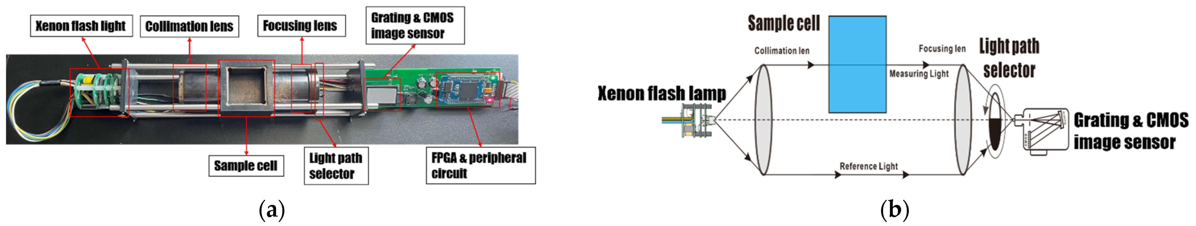
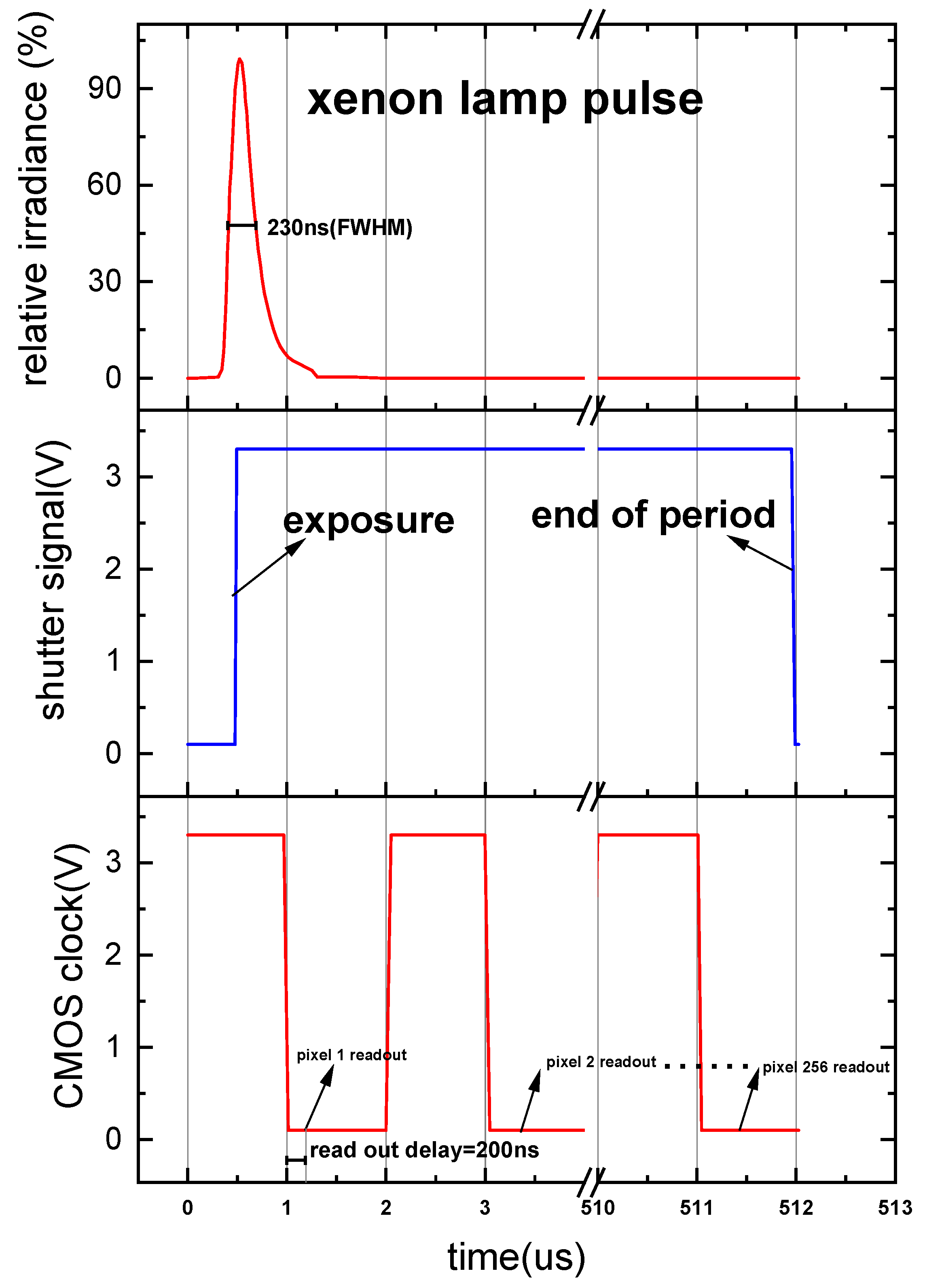
2.1. Experimental Setup

Figure 1 shows the physical structure and detailed optical path of the spectrophotometer. The hardware system can be divided into four major parts: a light source, an optical path, an optic sensor circuit and a data-processing circuit based on FPGA. A xenon flash light (L13821, Hamamatsu Photonics K.K., Shizuoka, Japan) that is controlled by pulse signal is selected as the light source. The optic sensor circuit is comprised of an integrated micro grating, CMOS image sensor (S8377, Hamamatsu Photonics K.K.) and its peripheral circuit. The light from the xenon flash light, collimated by a group of lenses, irradiates into the double optical path unit. The light into the upper path, called measurement light, passes through the sample pool, and the absorption occurs. The light into another path, called reference light, passes through the cavity without the sample pool. The light-path selector, a disk structure that is half covered by light shielding, is switched for determining which path light should be coupled into the optic-sensor unit. The collimated light of the measurement or reference path is dispersed by a grating and focused onto the CMOS image sensor. According to Lambert-Beer’s law [29], the absorption can be calculated by the following formula:
A = l o g T = l o g I 0 I = l o g U 0 U = ε × c × d
in which T is transmission; I 0 /   I is the intensity of the measuring light beam that is accepted by the CMOS sensor before/after passing through the sample; U 0 is the CMOS readout signal for the upper measuring light in Figure 1b and U is the CMOS signal for the lower reference light in Figure 1b; ε is the molar absorption coefficient; c is the concentration of the measured solution; and d is the path length of the measuring beam in the sample.
Figure 2 depicts the sequence diagrams of the capturing procedure for the xenon flash light. The trigger signal and 500 kHz clock are generated by FPGA to drive the xenon flash lamp and linear CMOS sensor, respectively. The lamp flashes when the trigger signal is at a high level. The light source takes time to reach the maximum light intensity and then declines until it extinguishes. The maximum irradiance of the xenon light appears when the trigger signal of the light source at a high level lasts for 0.5 μs. Meanwhile, the shutter signal of the linear CMOS sensor is set to a high level and the exposure occurs. The linear CMOS outputs the data of each pixel at the speed of 500 kHz, and the delay of the output of each pixel is 200 ns. Due to the fast response speed of the CMOS sensor, the spectrum can be quickly received by the sensor with just once flash of the xenon light. After the A/D converter, the pixel data from the CMOS sensor are received by FPGA and stored into the RAM in order. The address that stores the pixel data can be converted to the corresponding wavelength.

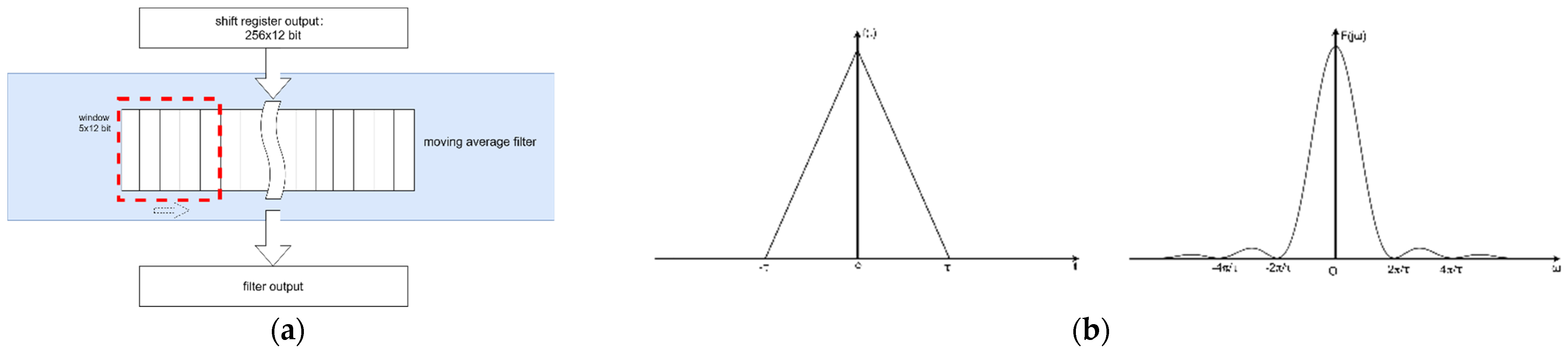
2.2. Moving-Average Filter Design for the Spectrum Data

Considering the input signals of infinite length x n ,   n = ,   ,   0 ,   1 ,   , the output of the moving-average filter is expressed as:
y n = 1 2 m + 1 k = n m n + m x n k
where m is the positive integer, 2 m + 1 is the order of the filter.
However, an infinite length signal does not exist in the engineering system. Thus, x n should be rewritten as x n ,   n = 0 ,   1 ,   N . From the expression 2 we can see that the filter has a delay of m points, which means that the corresponding output of the input x 0 is y m .Therefore, other outputs y 0 ,   y 1 ,   ,   y m 1 before the input x 0 are unsteady outputs of the filter and should be discarded.
The mathematical derivation of the frequency response of the moving-average filter is expressed as follows.
Considering the input signal is the unit impulse function:
h n = 1 ,  if  n = 0 0 ,  otherwise
The output of the moving-average filter is expressed as:
y n = 1 2 m + 1 k = n m n + m h n k
According to Fourier transformation theory, the unit-impulse response of the filter is expressed as follows:
H e j Ω = 1 2 m + 1 k = n m n + m e j k Ω = 1 2 m + 1 e j m Ω + e j m Ω + e j m 1 Ω + e j m 1 Ω + + ( e j Ω + e j Ω ) + 1 = 1 2 m + 1 1 + 2 k = 1 m cos k Ω
where:
Ω = w f s = 2 π f f s
Thus:
H e j × 2 π f s = 1 2 m + 1 1 + 2 k = 1 m cos k × 2 π f s
The sample rate f s in this design is equal to the linear CMOS image sensor readout frequency. Selection of the proper filter order is important for finding the best fitting of the spectrum data. The amplitude–frequency response curve at a different filter order should also be checked until the proper filter order is decided, according to the frequency distribution of the spectrum data.
A single spectrum peak signal is treated as a triangular pulse:
f t = 1 t τ ,   t < τ 0 ,    else
The spectrum peak signal is converted from time domain to frequency domain by using Fourier transformation; the amplitude-frequency function is:
F j ω = τ S a ω τ 2 2 = τ sin ω τ / 2 ω τ / 2 2
According to Rayleigh’s theorem, the energy-frequency spectrum of the signal is:
G ω = 1 π F j ω 2
The curve of F j ω is depicted in Figure 3b. Therefore, we can draw the conclusion that the main energy distribution band of the signal is in the range of 0 ~ 4 π / τ .

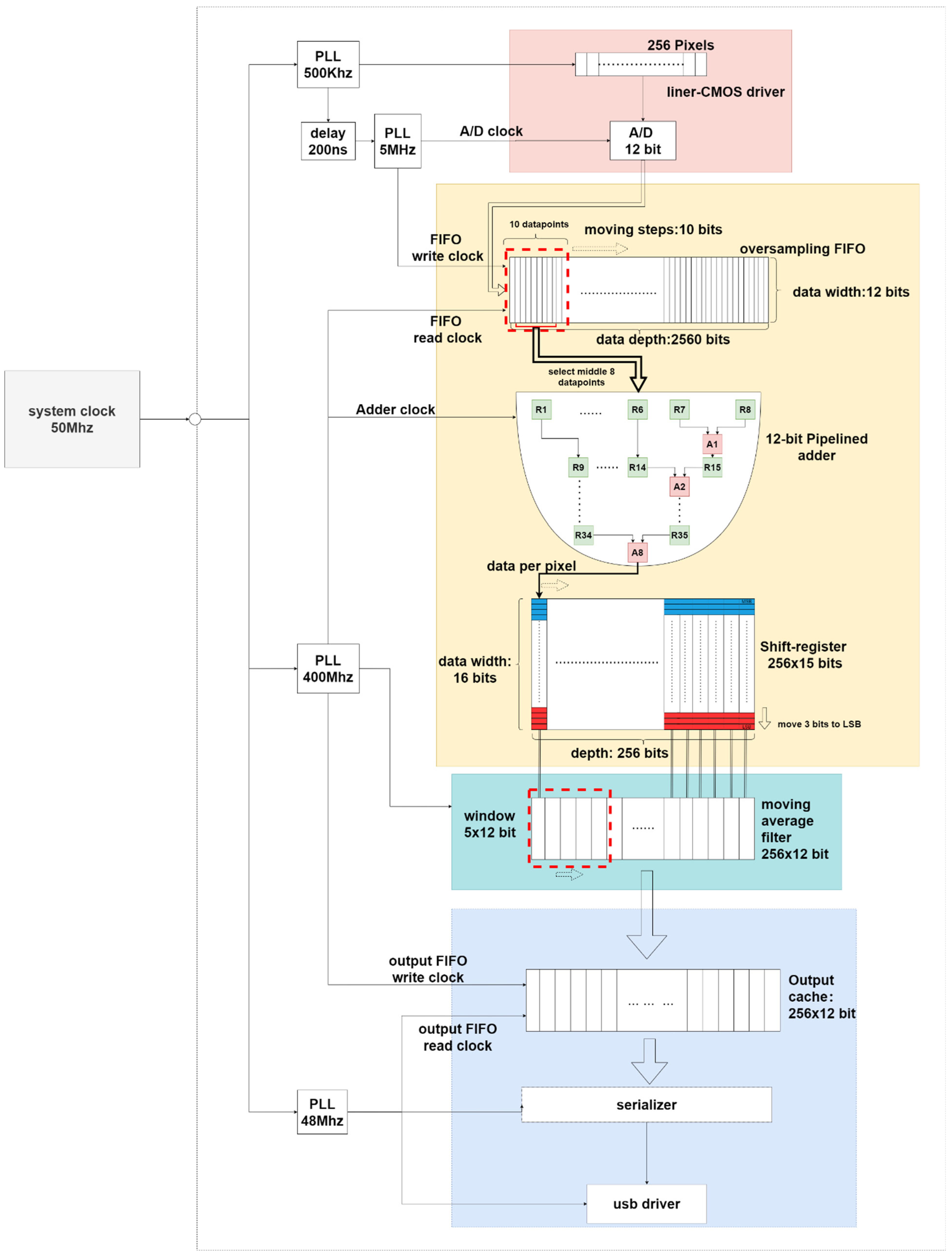
2.3. Implementation on the FPGA Board

The schematic diagram of the CMOS spectrophotometer system is depicted in Figure 4. The system is constructed on the FPGA chip (Spartan 6 XC6SLX16, Xilinx, San Jose, CA, USA). The oversampling method and the moving-average filter work under the synchronized clock at the frequency of 400 MHz, thereby increasing the processing speed to achieve real-time denoising. The system clock is set to different clock domains by a phase-locked-loop circuit. Meanwhile, multiple distributed RAMs and block RAMs are implemented to avoid metastability while the data are transferred through different clock domains.
An oversampling technology is implemented in this design. While the CMOS pixel data readout occurs at the frequency of 500 kHz, the A/D converter is driven by a 5 MHz clock to obtain 10 datapoints per pixel, with 200 ns delayed after the CMOS driver clock. Therefore, our measurements produce an origin 2560-datapoint dataset for all 256 pixels by this oversampling method. The oversampled data are stored in FIFO RAM and the average calculation of each pixel data is achieved. To adapt the shifting operation afterwards, 8 datapoints of each pixel are selected from 10 datapoints and sent to the adder to calculate the average output of each pixel from the oversampled data.
The adder for the FIFO RAM outputs is designed in an 8-stage pipelined architecture, which yields output in every clock period. Thus, the pipelined structure can increase the throughput of the FPGA to achieve the summation of the oversampled data at a fast speed, thereby achieving real-time denoising. In this pipelined design, after latency, one output is produced for every clock tick; thus, calculating the whole oversampled data from 256 CMOS pixels takes 256 + 7 = 263 clock periods at the frequency of 400 MHz. As a result, at a cost of 35 registers and 8 adders that are used in this pipelined structure design, the throughput of an FPGA is strongly increased, compared to the non-pipelined design.
The averaging function of the oversampling method is realized by deploying a shift register. For every clock tick (after latency), the output of the adder is loaded into the shift register. By applying right shift operation to the data in the different addresses, the spectrum data bits change from 15 to 12. The effect of averaging is to reduce the mean square noise per pixel. By computing the mean value of the oversampled data at each pixel, the random error from the linear CMOS is reduced as a function of N , following Gaussian statistics, where N is the number of oversampled datapoints per pixel.
However, the oversampled pixel data still contain a high level of noise—especially in the high-frequency domain, which cannot be eliminated by the oversampling technology—such as shot noise and circuit noise [18]. Thus, the moving-average filter that is designed in Section 2.2 is implemented. The filtered spectrum data are read out and stored at the output cache. Then, the data are sent to a personal computer through a USB interface at the band rate of 115,200 bit/s.

3. Results

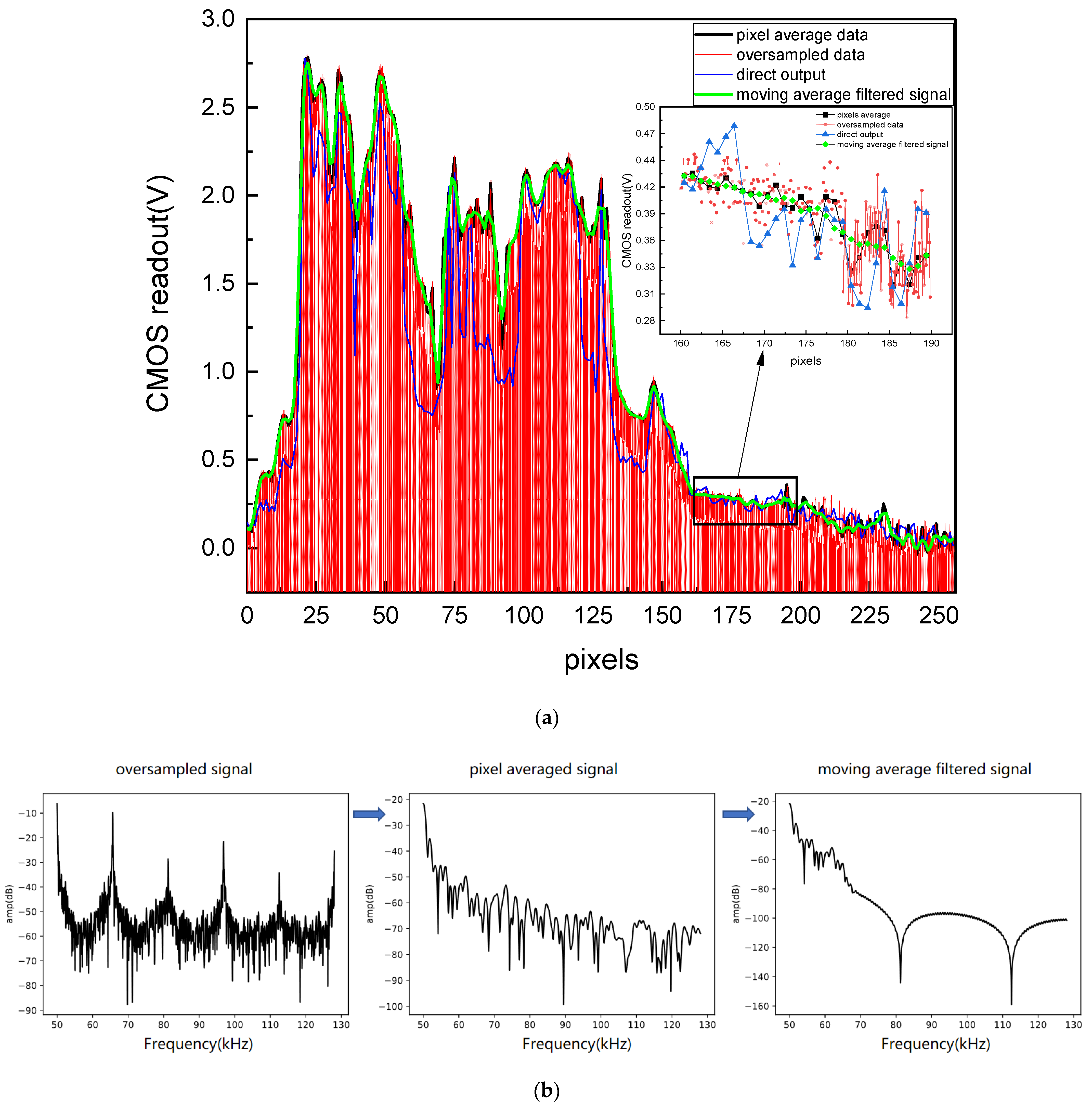
3.1. System’s Working Performance

The system’s working performance and the resource usage is shown in Table 1. The physical power consumption of the system is listed in Table 2. Power is measured by using the XPower Analyzer of the Xilinx ISE tool. The working frequency of the CMOS sensor is 500 kHz, and the CMOS sensor contains 258 pixels (including 256 effective pixels and two blank pixels). Thus, a full spectrum from the CMOS sensor consumes 1 / 500 × 258 = 0.516   ms = 516   μ s . The oversampling unit is synchronized with the CMOS readout signal, so the time latency is mainly contributed by the denoising module. The denoising module’s working frequency is 400 MHz. Thus, the time latency for an eight-stage pipelined adder is 1 / 400 × 256 + 7 = 0.6575   μ s . The shift register consumes 1 / 400 × 3 = 0.0075   μ s to complete right shift operation. The time latency of the moving-average filter is 1 / 400 × 260 = 0.65   μ s because the sum of the spectrum datapoints after filtering is 256 + 5 1 = 260 . As a result, the proposed denoising algorithm works in real time because the time latency from the denoising method is far less than one CMOS senor read-out period, which is 516   μ s .

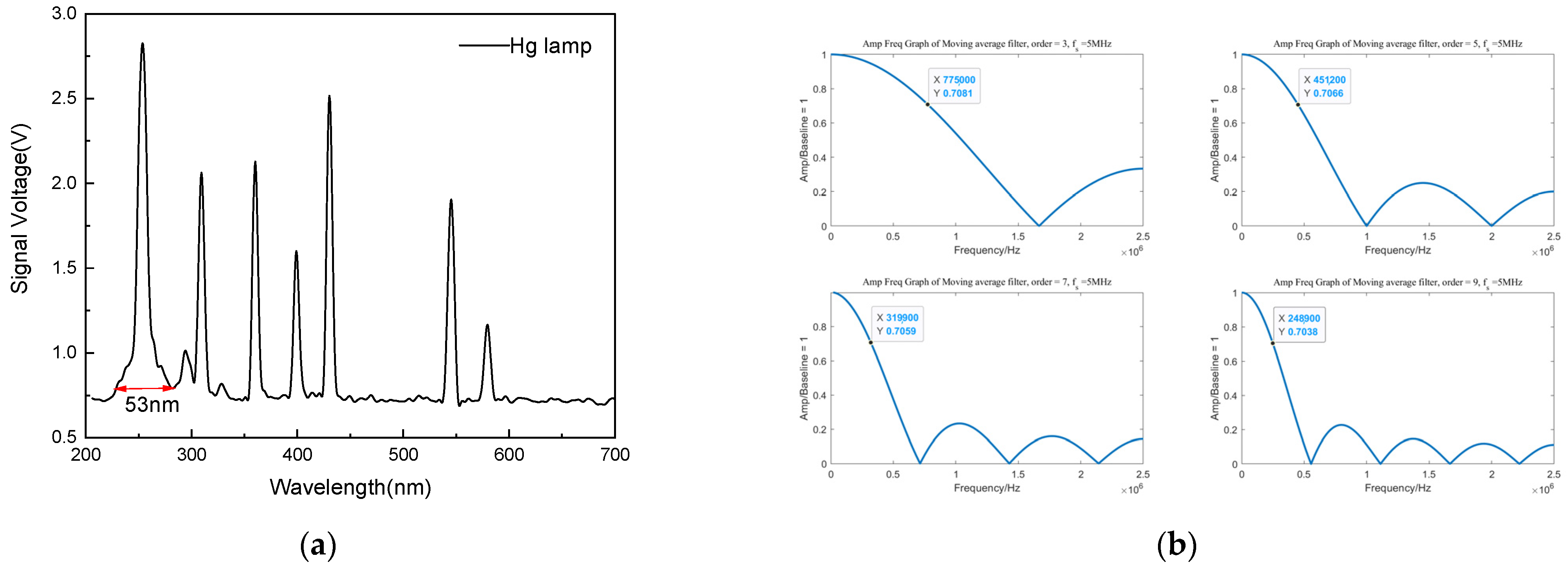
3.2. Determination of the Filter Parameters

In this section, the parameters of the filter are set adaptively by evaluating the spectral resolution of the CMOS-based spectrophotometer system. The specific order of the filter is determined by measuring the full width of the spectrum pulse when the pulse’s peak reaches the CMOS sensor’s saturation voltage. A Hg lamp is used as a light source in this determination process because it has line spectra and an abundant characteristic spectrum. The pulse spectrum of the Hg lamp is broadened because of the limited resolution of the measuring system. Thus, the full width of the saturated spectrum pulse indicates the characteristic of the system function. The measured spectrum profile of the Hg lamp is a convolution result between the input pulse spectrum of the light source and the function of this electro-optical system. From Figure 5a, we can see that the highest spectrum peak appears at the wavelength of 253 nm, and the width of the highest spectrum peak is 53 nm. The wavelength range of the light that is dispersed by the optical grating is from 200 nm to 700 nm. Thus, the wavelength gap is 700 200 / 256 = 1.9 nm   between two adjacent pixels. Hence, the width of the spectrum peak can be converted to the numbers of pixels, which is 53 / 1.9 = 27.9 pixels.
Since the width of the spectrum peak in the time domain is 2τ, in this case, τ = 27.9 × 1 500 , 000 × 1 2 = 27.9   μ s , which corresponds to the frequency of valid information of the spectrum, as calculated before.
According to the graph of F j ω , we know that in order to obtain the major energy of the signal and efficiently filter the high-frequency noise, the angular frequency of the filter’s cutoff point f must be between 2 π τ × 1 2 π = 1 / τ and 4 π τ × 1 2 π = 2 / τ , which means that the frequency of the filter’s cutoff point is between 35,842 Hz and 71,684 Hz, according to the amplitude–frequency response curve of the filter. Thus, a five-orders moving-average filter is selected in this system by considering a 3 dB power point as the cutoff point.

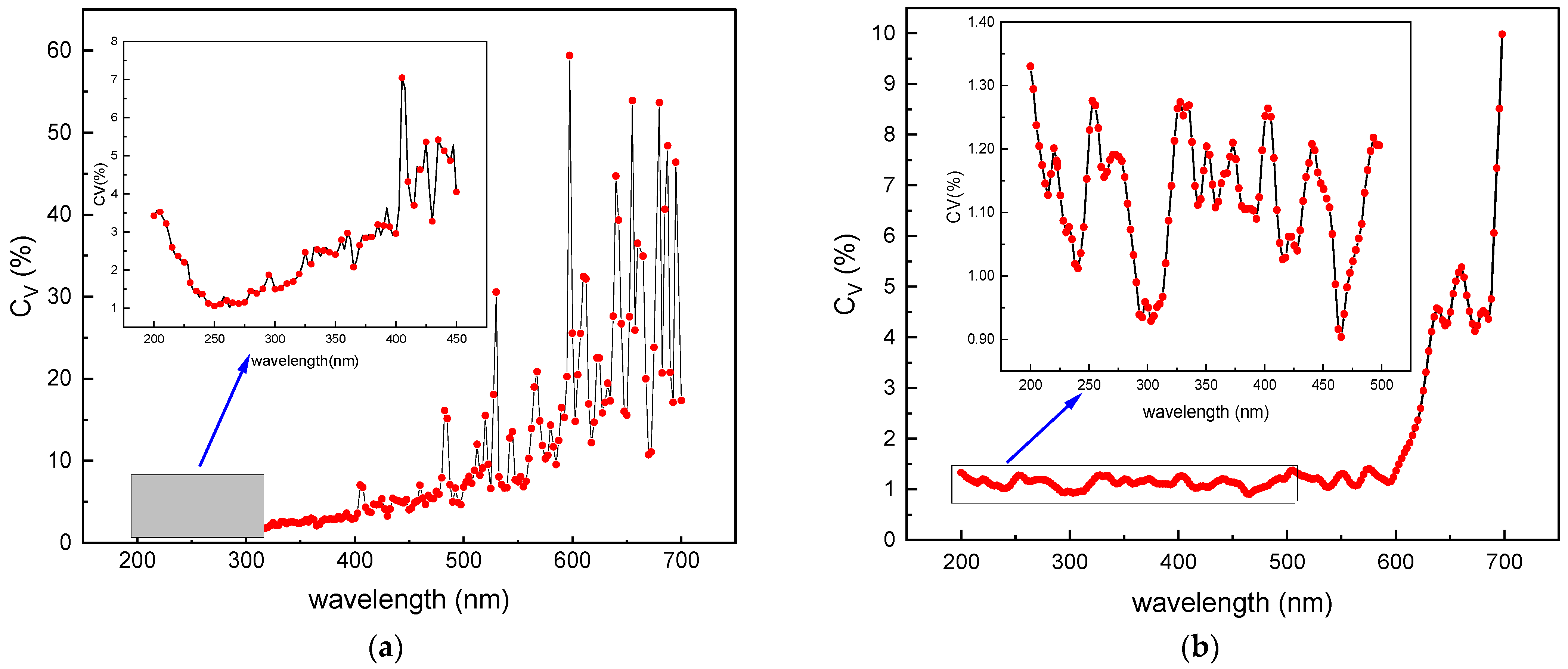
3.3. Noise Evaluation for the Spectrum of Xenon Flash Light

In this section, we measure the spectrum of a xenon flash light and evaluate the noise performance of each denoising stage. The main discharge voltage of xenon flash lamp is 400 V.
The signal comparison between the direct output of the CMOS image sensor, the average result from the oversampled data, and the signal that is filtered by the moving-average digital filter is illustrated in Figure 6a. In the figure, the “Direct output” is the CMOS sensor’s pixel signal directly read by the data acquisition system on FPGA, and each pixel produces one voltage signal. The “Oversampled data” is the pixel signal when the ADC chip’s write speed is 10-times faster than the CMOS sensors’ readout speed. Under this condition, each pixel produces 10 voltage signals. The “Pixel average data” is the mean result of the 10 voltage signals that each pixel produces after the oversampling operation. Thus, it can represent the voltage level of each pixel more precisely. The “Moving average filtered signal” is the filter result after the “oversampled data” passes through the moving-average digital filter. Signals from the 160th pixel to the 190th pixel were enlarged in the smaller image because the corresponding spectrum wavelength of the 160th pixel to the 190th pixel was 512 nm to 571 nm, where no obvious spectrum peak of xenon flash light existed in this wavelength range, so that the effect of noise was obvious to observe. As can be seen, the signal that was obtained from a single pixel (blue line) had a significant loss on the signal amplitude, whereas the signal that was obtained from an average of oversampled data (black line) had less amplitude loss, especially in the range of ultra-violet wavelength. The signal after passing the moving-average digital filter (green line) had much-reduced noise.
To further evaluate the noise of the spectrum, the comparison of the spectrum signal was made in the frequency domain using 2048-point fast Fourier transform (FFT) in Figure 6b. The figure shows that the origin signal consisted of a valid CMOS signal, the noise floor and some other spurious frequencies that were below −40 dB. At the frequency points of 60 kHz, 80 kHz, 95 kHz, 115 kHz and 130 kHz, the peak of the alias frequency appeared. These peaks, which are produced by the sum or difference between the fundamental frequencies and sensor noise, including their harmonics, consisted of additional high-order tones. While these tones may exist beyond the signal bandwidth of interest, they can still alias into the ADC passband and degrade AC specs such as SNR. After the averaging calculation of 10 datapoints to each pixel was deployed, the peak of the alias frequency disappeared, and the noise floor fell from −60 dB to −80 dB, which meant that the sensor noise was greatly reduced, and the harmonics were observably eliminated. After the pixel averaging calculation, the moving-average filter was deployed to the spectrum data. From the time-domain graphic of the signal, the valid spectral-peak information of the original signal was well preserved, while the denoised signal was smoother than the origin signal. From the frequency-domain graphic of the signal, we can see that the high-frequency component of the signal was much more suppressed from −80 dB to −140 dB, while in the signal bandwidth of interest around 60 kHz, the amplitude of the signal hardly declined.
To specifically evaluate the reduction in the noise and the stability of the system, the coefficient of variation ( C v ) is introduced and defined as below:
C v = σ μ × 100 %
σ is the standard deviation of the samples and μ is the average value of the samples. The coefficient of variation ( C v ) shows the dispersion degree of the measurement and can reflect the stability of the instrument. The spectrum signal at each wavelength was tested 40 times to calculate C v , using deionized water as a tested solution. Figure 7a,b show the global C v comparison at a wavelength range of 200~700 nm. The result shows that the stability of the system was greatly improved at all UV-Vis wavelengths after the digital filter was implemented, especially at the wavelength of the visible light range. The average coefficient of variation of the measurements in all wavelengths (200~700 nm) was reduced from 9.57% to 1.74%, which reached the average accuracy of the common online UV-Vis instruments for water-quality monitoring [30]. The maximum C v , which indicated the worst case of the measurement, was reduced from 59.38% to 9.79%.
Figure 8a shows the CMOS sensor’s relative sensitivity at different wavelengths, given by the manufacturer (Hamamatsu Photonics K.K.). To ensure the validity of the measured spectrum for the xenon flash light, the measured spectrum of the light source was recalculated and normalized by taking the image sensor’s sensitivity into consideration. The comparison was made between the recalculate spectrum and the standard spectrum dataset that was given by the manufacturer (Hamamatsu Photonics K.K.) in Figure 8b. As can be seen from the plot, the consistency exists between two spectrums’ profiles. However, due to the resolution limitation of the optical grating and CMOS image sensor, some details of the spectrum were lost.
The result shows that the CMOS linear image sensor successfully captured the spectrum of the xenon flash light within a single flash at the readout clock frequency of 500 kHz, and the real-time denoising method based on the FPGA effectively ensured the stability of the system running at the clock frequency of 400 MHz.

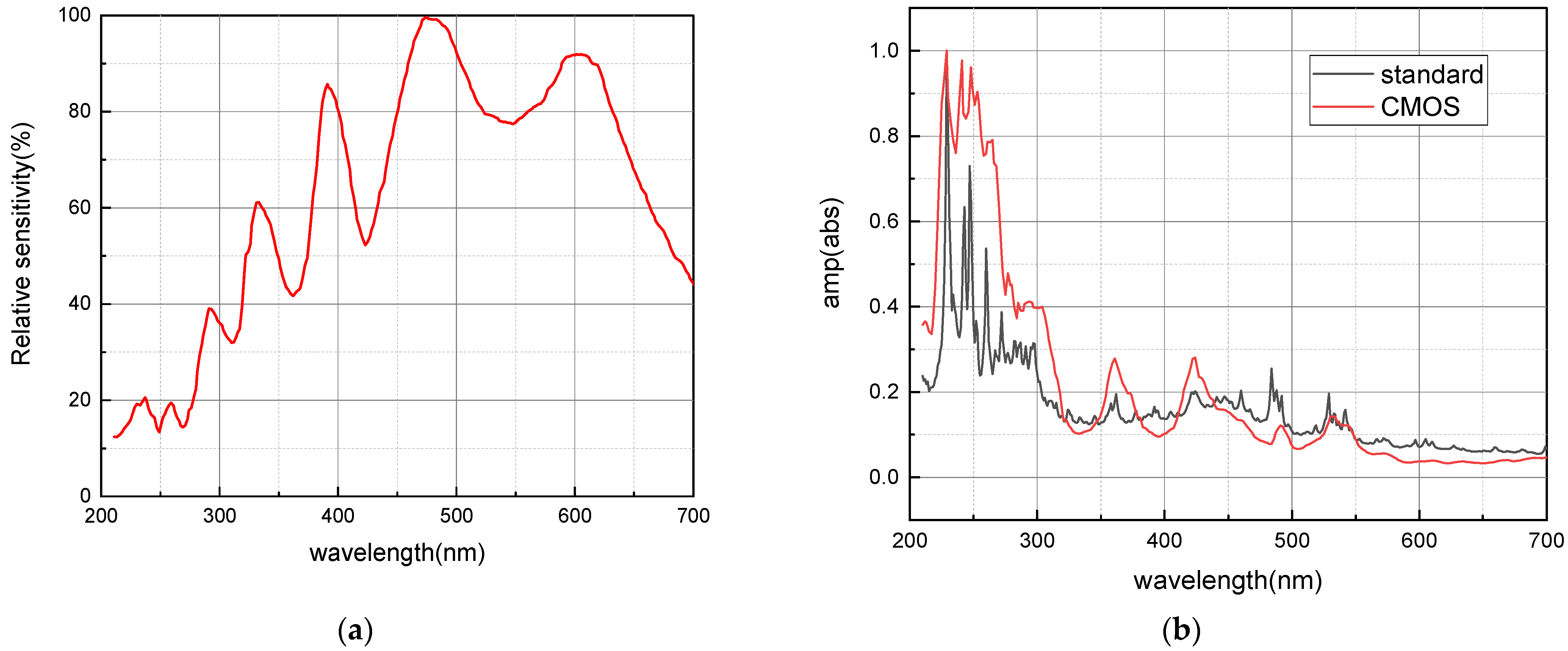
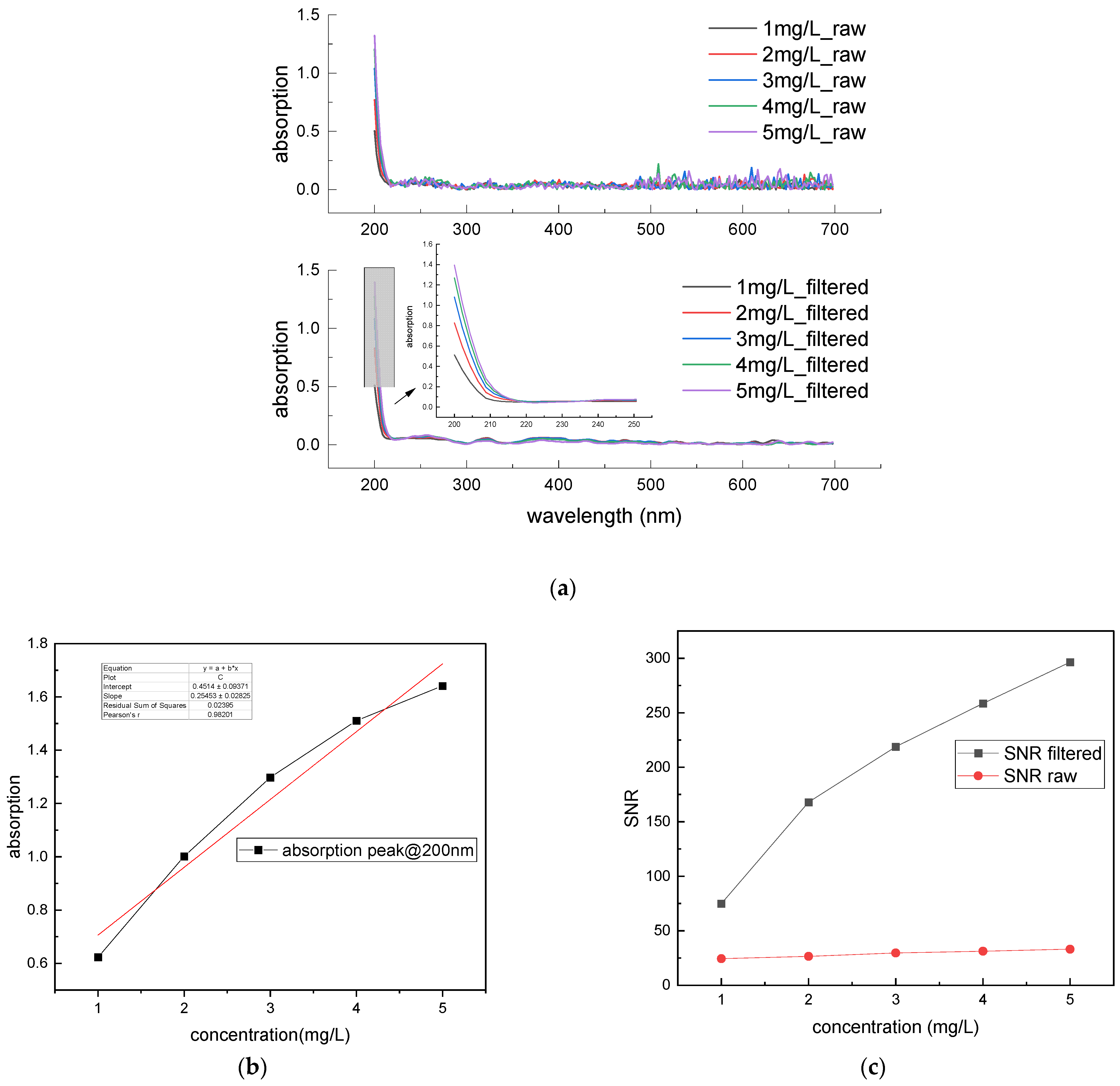
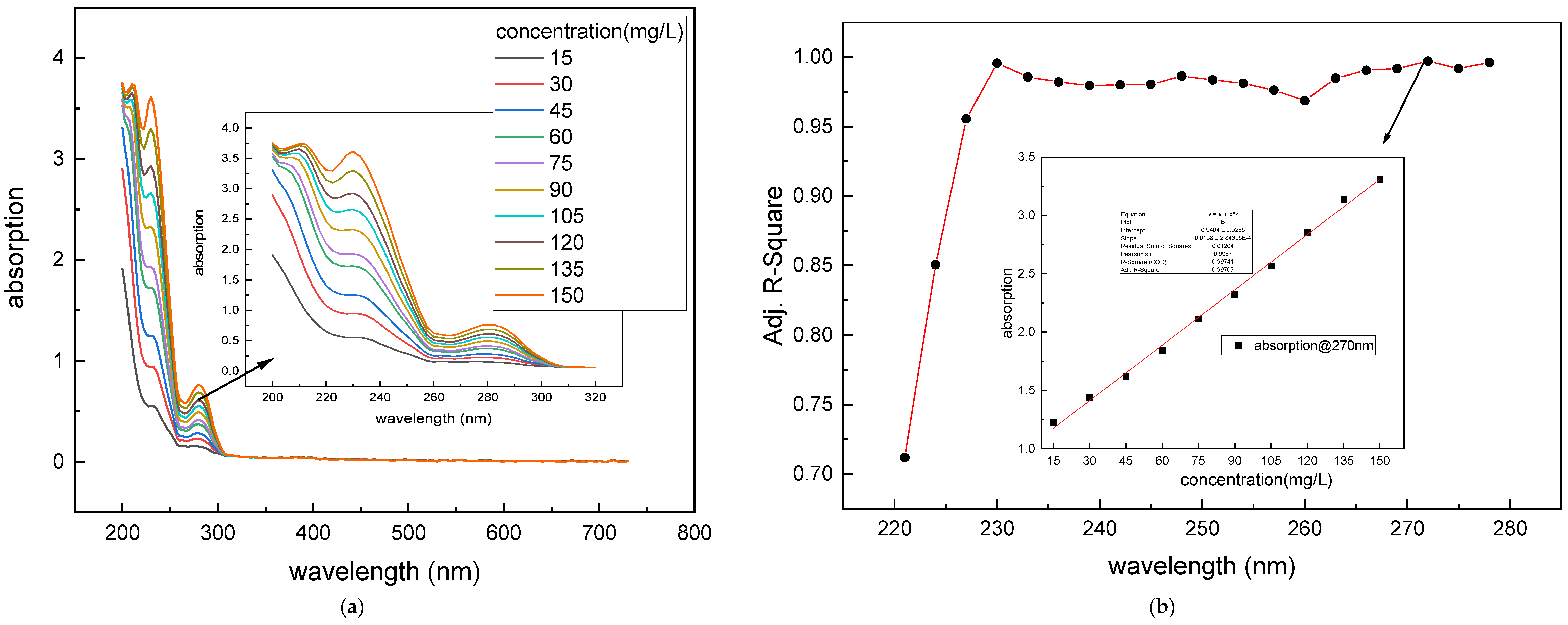
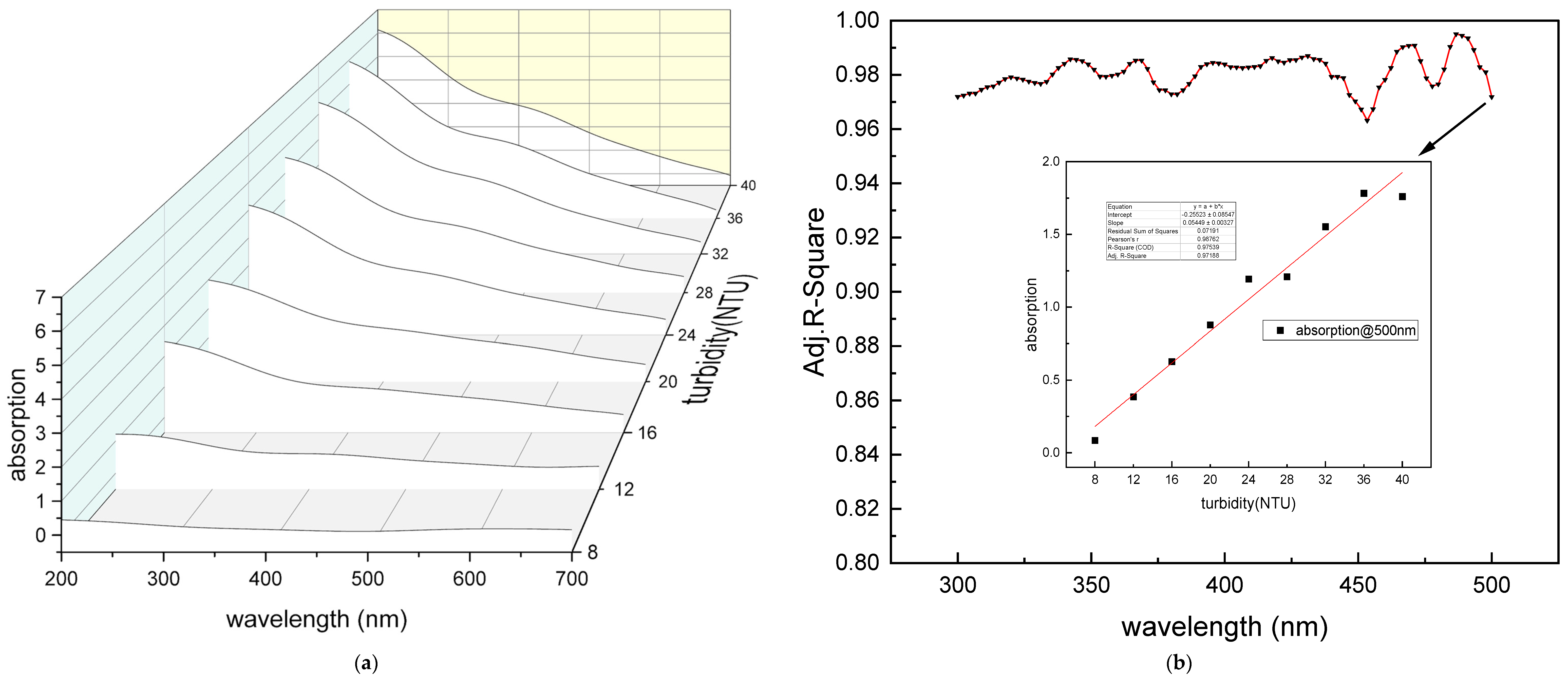
3.4. Signal Quality Evaluation for Absorption Spectrum

In this section, we have quantified several analytes in solution and measured the absorption spectrum with the spectrophotometer that we designed. All the experiments were performed using a quartz cell with an optical path length of 20 mm, and the main discharge voltage of the xenon flash lamp was 600 V.
SNR is an important metric for establishing signal quality in all fields of engineering, and it is employed here to evaluate the spectrum quality. The SNR in spectrum is commonly defined as the ratio of the true signal maximum intensity to the standard deviation of the noise. The wavelength position of the maximum absorption intensity depends on the different chemical bond of the dissolved matter. In order to evaluate the SNR of the system, the nitrate solution of different concentrations was prepared by dissolving potassium nitrate into the deionized water, which was supplied by a MilliQ water purification system (Millipore, Billerica, MA, USA). The absorption peak of the nitrate occurs at the wavelength range of 200~210 nm under the condition of low concentration [31]. The nitrate solution was divided into five groups from 1 mg/L to 5 mg/L. Thus, the noise is estimated by calculating the root mean square (RMSE) of the intensity at the wavelength in the range of 500~700 nm, where nitrate has no contribution to the absorption spectrum and the baseline of the noise can be easily determined. The SNR is defined as follows:
S N R x i = max x i R M S E x r e f
R M S E x r e f = 1 N i = 500 n m N x i r e f x r e f ¯ 2
where x i r e f is the specific spectrum value at the wavelength;   x r e f ¯ is the average value of the spectrum signal at the wavelength range of 500~700 nm; x i is the characteristic spectrum peak of the specific matter; and N is the number of datapoints between the wavelength of 500 nm and 700 nm.
The calculation results of the absorption peak, RMSE value and SNR value of the filtered spectrum data and raw spectrum data are listed in Table 3. At the condition of the 5 mg/L nitrate solution, the RMSE noise of the absorption spectrum decreased from 0.04279 to 0.00554. The filtered absorption spectrum data and raw absorption spectrum data of nitrate in concentration ranging from 1 mg/L to 5 mg/L are illustrated in Figure 9a. The SNR variation in the nitrate solution is depicted in Figure 9c. After the filter was implemented, the SNR greatly improved by nine times at the concentration of 5 mg/L.
Another important indicator for the absorption spectrophotometer is the linearity between the absorption intensity and concentration [32]. According to Lambert-Beer’s law, when the length of the light path is constant, the characteristic absorption intensity of the substance and concentration should be agreed with a linear function. The fitting results in Figure 9b indicate that the nitrate concentration shows good linearity with the absorption magnitude value when the concentration of nitrate is below 4 mg/L. However, the linear relation becomes slightly lost when the concentration of nitrate is above 4 mg/L. This is because the average distance between absorbing components shrinks at the high concentration, and the charge distribution between adjacent particles is affected, changing their absorption capacity for specific radiation [33]. The higher the concentration is, the greater the deviation becomes [34].
We then measured the absorption spectrum of the chemical oxygen demand (COD) solution at the concentration range of 15 mg/L to 150 mg/L in 10 groups. The COD solution of different concentrations was prepared by dissolving the potassium hydrogen phthalate into the deionized water; the result is illustrated in Figure 10a. The result shows that each nitrate concentration has a well-differentiated absorption magnitude in the wavelength range from 230 nm to 280 nm. The linear fitting procedure between the COD concentration and the absorption value was completed at each wavelength in a range from 230 nm to 280 nm, and the coefficient of determination (adjusted R-Square values) at each wavelength is illustrated in Figure 10b. The result shows that at the wavelength of 270 nm, the concentration of COD shows the best linearity with the absorption magnitude, and the adjusted R-Square value at this wavelength is beyond 0.99.
To further evaluate the performance of the system in the wavelength of visible band (400~700 nm), the solution was selected as an analyte sample, due to the absorption of turbidity that occurs both at the ultra-violet band and the visible band of the spectrum [35]. The turbidity solution was diluted from the Formazine solution at the concentration of 400 NTU and divided into nine groups at the concentration range from 8 NTU to 40 NTU. Figure 11a shows the absorption spectrum of turbidity in different concentrations. The adjusted R-Square values between the turbidity concentration and the absorption value are illustrated in Figure 11b. Each adjusted R-Square value at the wavelength from 300 nm to 500 nm was calculated following the same linear fitting program. The result shows that all adjusted R-Square values at the wavelength range of 300~500 nm are above 0.95, which indicates that the absorption magnitude shows good linearity with the turbidity concentration in the visible band.

4. Discussion

Based on the designed hardware and optical structure, the CMOS linear image sensor successfully captured the spectrum of the xenon flash light within a single flash at the readout clock frequency of 500 kHz. The digital filter and the denoising method for the CMOS sensor is implemented on FPGA and works effectively to reduce the noise of the spectrum operating in real time at the clock frequency of 400 MHz, optimized by using a pipelined structure and dual high-speed FIFO RAM to match the high-speed rate of the CMOS sensor output in an in situ measurement application, which leads to a faster processing speed for the spectrum data.
An oversampling method that is suitable for the CMOS sensor’s output is proposed to reduce the sensor’s dark current noise and read noise. Moving-average filtering is performed on the low-frequency component to filter out the residual spectrum noise in the low-frequency components of the spectrum signal. The parameters of the filter are set adaptively by evaluating the spectral resolution of the CMOS-based spectrophotometer system, and a Fourier transform analysis is used for the spectrum data to avoid the problem of insufficiently clean filtering or the destruction of spectrum details as a result of fixed parameter settings. The coefficient of variation of the measurements is reduced from 9.57% to 1.74%, while the SNR of the absorption spectrum increases nine times or more, compared to the raw data of the CMOS sensor’s output. Tests towards different analyte samples were conducted, and the adjusted R-Square results indicated the good performance on distinguishing different concentrations of different analyte solutions on both ultra-violet and visible spectrum bands.

Author Contributions

Investigation, Methodology, Formal Analysis, Writing—Original Draft, Validation, M.X.; Methodology, Review and Editing, Funding Acquisition, G.Y.; Supervision, Conceptualization, Funding Acquisition, N.Z.; Writing—review and editing, Funding Acquisition, R.Y.; Investigation, X.C.; Investigation, C.F.; Investigation, M.D. All authors have read and agreed to the published version of the manuscript.

Funding

This research was funded by: Science and Technology Major Project of the Ministry of Science and Technology of Anhui Province, grant number (202003a07020007); Key Fusion Program of Special Foundation of President of Hefei Institutes of Physical Science, Chinese Academy of Sciences, grant number (YZJJZX202009); Instrument and Equipment Function Development Program of the Chinese Academy of Science, grant number (E03HBF11291); National Key Research and Development Program (2017YFF0108402).

Institutional Review Board Statement

Not applicable.

Informed Consent Statement

Not applicable.

Data Availability Statement

The data that support the findings of this study are available from the corresponding author upon reasonable request.

Acknowledgments

We thank Mingjun Ma and Liujun Zhong for their guidance in the optical and mechanical design.

Conflicts of Interest

The authors declare no conflict of interest.

References

  1. Li, S.; An, Y. Statistics of environmental events in China during the period from July to August in 2015. J. Saf. Environ. 2015, 15, 390–394. [Google Scholar]
  2. Li, Z.H.; Jia, J.J.; Wu, Y.S.; Zong, H.B.; Zhang, G.A.; Wang, Y.P.; Yang, Y.; Zhou, L.; Gao, S. Vertical Distributions of Suspended Sediment Concentrations in the Turbidity Maximum Zone of the Periodically and Partially Stratified Changjiang Estuary. Estuaries Coasts 2019, 42, 1475–1490. [Google Scholar] [CrossRef]
  3. Zhang, W.L.; Lei, M.T.; Li, Y.; Wang, P.F.; Wang, C.; Gao, Y.; Wu, H.N.; Xu, C.; Niu, L.H.; Wang, L.F.; et al. Determination of vertical and horizontal assemblage drivers of bacterial community in a heavily polluted urban river. Water Res. 2019, 161, 98–107. [Google Scholar] [CrossRef] [PubMed]
  4. Gong, J.; Ran, Y.; Zhang, D.N.; Chen, D.Y.; Li, H.Y.; Huang, Y.D. Vertical profiles and distributions of aqueous endocrine-disrupting chemicals in different matrices from the Pearl River Delta and the influence of environmental factors. Environ. Pollut. 2019, 246, 328–335. [Google Scholar] [CrossRef] [PubMed]
  5. Pons, M.-N.; Assaad, A.; Oucacha, C.; Pontvianne, S.; Pollier, B.; Wagner, P.; Legout, A.; Guérold, F. Nitrates monitoring by UV–vis spectral analysis. Ecohydrol. Hydrobiol. 2017, 17, 46–52. [Google Scholar] [CrossRef]
  6. Hu, Y.T.; Wen, Y.Z.; Wang, X.P. Detection of Water Quality Multi-Parameters in Seawater based on UV-Vis Spectrometry. In Proceedings of the Oceans 2016—Shanghai, Shanghai, China, 10–13 April 2016. [Google Scholar]
  7. Carter, H.T.; Tipping, E.; Koprivnjak, J.F.; Miller, M.P.; Cookson, B.; Hamilton-Taylor, J. Freshwater DOM quantity and quality from a two-component model of UV absorbance. Water Res. 2012, 46, 4532–4542. [Google Scholar] [CrossRef] [Green Version]
  8. Langergraber, G.; Gupta, J.K.; Pressl, A.; Hofstaedter, F.; Lettl, W.; Weingartner, A.; Fleischmann, N. On-line monitoring for control of a pilot-scale sequencing batch reactor using a submersible UV/VIS spectrometer. Water Sci. Technol. 2004, 50, 73–80. [Google Scholar] [CrossRef]
  9. Wu, D.; Wei, B.; Tang, G.; Feng, P.; Tang, Y.; Liu, J.; Xiong, S. Turbidity Disturbance Compensation for UV-VIS Spectrum of Waterbody Based on Mie Scattering. Acta Opt. Sin. 2017, 37, 0230007. [Google Scholar]
  10. Østergaard, J. UV/Vis Spectrophotometry and UV Imaging. In Analytical Techniques in the Pharmaceutical Sciences; Müllertz, A., Perrie, Y., Rades, T., Eds.; Springer: New York, NY, USA, 2016; pp. 3–27. [Google Scholar]
  11. Tian, P.; Qin, Y.H.; Zhao, L.; Mutisya, S.M.; Jin, J.H.; Lu, J.Q.; Hu, X.H. Multiparameter Spectrophotometry Platform for Turbid Sample Measurement by Robust Solutions of Radiative Transfer Problems. IEEE Trans. Instrum. Meas. 2021, 70, 6003110. [Google Scholar] [CrossRef]
  12. Hutchison, C.D.M.; Parker, S.; Chukhutsina, V.; van Thor, J.J. Open hardware microsecond dispersive transient absorption spectrometer for linear optical response. Photochem. Photobiol. Sci. 2022, 21, 23–35. [Google Scholar] [CrossRef]
  13. Fossum, E.R.; Hondongwa, D.B. A Review of the Pinned Photodiode for CCD and CMOS Image Sensors. IEEE J. Electron. Devices Soc. 2014, 2, 33–43. [Google Scholar] [CrossRef]
  14. Lourenco, N.D.; Paixao, F.; Pinheiro, H.M.; Sousa, A. Use of Spectra in the Visible and Near-Mid-Ultraviolet Range with Principal Component Analysis and Partial Least Squares Processing for Monitoring of Suspended Solids in Municipal Wastewater Treatment Plants. Appl. Spectrosc. 2010, 64, 1061–1067. [Google Scholar] [CrossRef] [PubMed]
  15. Helmers, H.; Schellenberg, M. CMOS vs. CCD sensors in speckle interferometry. Opt. Laser Technol. 2003, 35, 587–595. [Google Scholar] [CrossRef]
  16. Wang, Y.; Wan, B.; Fu, G.C.; Su, Y.T. PRNU Estimation of Linear CMOS Image Sensors That Allows Nonuniform Illumination. IEEE Trans. Instrum. Meas. 2021, 70, 5011711. [Google Scholar] [CrossRef]
  17. Fujihara, Y.; Murata, M.; Nakayama, S.; Kuroda, R.; Sugawa, S. An Over 120 dB Single Exposure Wide Dynamic Range CMOS Image Sensor With Two-Stage Lateral Overflow Integration Capacitor. IEEE Trans. Electron. Devices 2021, 68, 152–157. [Google Scholar] [CrossRef]
  18. Janesick, J.R.; Elliott, T.; Collins, S.; Blouke, M.M.; Freeman, J. Scientific Charge-Coupled-Devices. Opt. Eng. 1987, 26, 692–714. [Google Scholar] [CrossRef]
  19. Al-Rawhani, M.A.; Cheah, B.C.; Macdonald, A.I.; Martin, C.; Hu, C.X.; Beeley, J.; Gouveia, L.C.; Grant, J.P.; Campbell, G.; Barrett, M.P.; et al. A Colorimetric CMOS-Based Platform for Rapid Total Serum Cholesterol Quantification. IEEE Sens. J. 2017, 17, 240–247. [Google Scholar] [CrossRef] [Green Version]
  20. Liu, L.; Zhang, X.-l.; Huang, D.-x. Measurement method for semiconductor optical amplifier gain coefficient with wavelet denoise and deconvolution. Chin. J. Lasers 2007, 34, 846–850. [Google Scholar]
  21. Li, J.W.; Tong, Y.F.; Guan, L.; Wu, S.F.; Li, D.B. A UV-visible absorption spectrum denoising method based on EEMD and an improved universal threshold filter. RSC Adv. 2018, 8, 8558–8568. [Google Scholar] [CrossRef] [Green Version]
  22. Xie, C.F.; Wang, P.; Cai, C.J.; Zhang, Y.B.; Shi, J.L.; He, X.D. A Simple and accurate method for Brillouin spectroscopy based on virtual imaging phased array spectrometer and charge-coupled device cameras. Opt. Commun. 2021, 488, 126821. [Google Scholar] [CrossRef]
  23. Ferreira, J.L.; Wu, Y.; Aarts, R.M. Enhancement of the Comb Filtering Selectivity Using Iterative Moving Average for Periodic Waveform and Harmonic Elimination. J. Healthc. Eng. 2018, 2018, 7901502. [Google Scholar] [CrossRef] [PubMed] [Green Version]
  24. Allen, P.J.; Josephs, O.; Turner, R. A method for removing imaging artifact from continuous EEG recorded during functional MRI. Neuroimage 2000, 12, 230–239. [Google Scholar] [CrossRef] [PubMed] [Green Version]
  25. Laurent, G.; Gilles, P.A.; Woelffel, W.; Barret-Vivin, V.; Gouillart, E.; Bonhomme, C. Denoising applied to spectroscopies—Part II: Decreasing computation time. Appl. Spectrosc. Rev. 2020, 55, 173–196. [Google Scholar] [CrossRef] [Green Version]
  26. Athi, M.V.; Zekavat, S.R.; Struthers, A.A. Real-Time Signal Processing of Massive Sensor Arrays via a Parallel Fast Converging SVD Algorithm: Latency, Throughput, and Resource Analysis. IEEE Sens. J. 2016, 16, 2519–2526. [Google Scholar] [CrossRef]
  27. Pham, Q.A.; Lopez-Bueno, D.; Wang, T.; Montoro, G.; Gilabert, P.L. Partial Least Squares Identification of Multi Look-Up Table Digital Predistorters for Concurrent Dual-Band Envelope Tracking Power Amplifiers. IEEE Trans. Microw. Theory Tech. 2018, 66, 5143–5150. [Google Scholar] [CrossRef] [Green Version]
  28. Qassim, Y.T.; Cutmore, T.R.H.; Rowlands, D.D. Optimized FPGA based continuous wavelet transform. Comput. Electr. Eng. 2016, 49, 84–94. [Google Scholar] [CrossRef] [Green Version]
  29. Skoog, D.A.; Holler, F.J.; Crouch, S.R. Principles of Instrumental Analysis; Cengage Learning: Boston, MA, USA, 2017. [Google Scholar]
  30. Shi, Z.N.; Chow, C.W.K.; Fabris, R.; Liu, J.X.; Jin, B. Applications of Online UV-Vis Spectrophotometer for Drinking Water Quality Monitoring and Process Control: A Review. Sensors 2022, 22, 2987. [Google Scholar] [CrossRef]
  31. Otten, D.E.; Petersen, P.B.; Saykally, R.J. Observation of nitrate ions at the air/water interface by UV-second harmonic generation. Chem. Phys. Lett. 2007, 449, 261–265. [Google Scholar] [CrossRef]
  32. Mantele, W.; Deniz, E. UV-VIS absorption spectroscopy: Lambert-Beer reloaded. Spectrochim. Acta A Mol. Biomol. Spectrosc. 2017, 173, 965–968. [Google Scholar] [CrossRef]
  33. Kortum, G. The optical behaviour of solute ions and its significance for the structure of electrolytical solutions. IV The scope of Lambert-Beer’s law in watery solutions of anorganic salts. Z. Fur Phys. Chem. Abt. B Chem. Der Elem. Aufbau Der Mater. 1936, 33, 243–264. [Google Scholar]
  34. Mosorov, V. The Lambert-Beer law in time domain form and its application. Appl. Radiat. Isot. 2017, 128, 1–5. [Google Scholar] [CrossRef] [PubMed]
  35. Chen, X.W.; Yin, G.F.; Zhao, N.J.; Gan, T.T.; Yang, R.F.; Xia, M.; Feng, C.; Chen, Y.A.; Huang, Y. Simultaneous determination of nitrate, chemical oxygen demand and turbidity in water based on UV-Vis absorption spectrometry combined with interval analysis. Spectrochim. Acta Part A Mol. Biomol. Spectrosc. 2021, 244, 118827. [Google Scholar] [CrossRef] [PubMed]
Figure 1. (a) Physical structure of the implemented spectrophotometer platform. (b) Schematic of the fused double-beam structure.
Chemosensors 10 00282 g001
Figure 2. Timing schematic of the working procedure showing how the CMOS image sensor captures the xenon flash.
Chemosensors 10 00282 g002
Figure 3. (a) Structure of the moving-average filter on FPGA. (b) Determination of the filter orders for the spectrum data using Fourier transformation.
Chemosensors 10 00282 g003
Figure 4. Schematic diagram of the CMOS driver unit, spectral data processing unit and data transmission unit of the spectrophotometer on the FPGA board.
Chemosensors 10 00282 g004
Figure 5. (a) Determination of the valid spectrum signal frequency using Hg lamp spectrum measured by this system. (b) Amplitude–frequency response curve at different filter orders of the moving-average filter.
Chemosensors 10 00282 g005
Figure 6. (a) Comparison of the readout spectrum data between the direct output of the CMOS image sensor, the average result from the oversampled data and the signal filtered by moving-average filter. (b) Comparison of the spectrum signal in frequency domain after pixels averaging and digital filter are deployed.
Chemosensors 10 00282 g006
Figure 7. (a) Global coefficient of variation of the unfiltered data. (b) Global coefficient of variation of the filtered data.
Chemosensors 10 00282 g007
Figure 8. (a) CMOS sensor’s relative sensitivity. (b) Spectrum comparison of xenon lamp between standard dataset and the CMOS-based system.
Chemosensors 10 00282 g008
Figure 9. (a) Filter result for absorption spectrum of nitrate in concentration from 1~5 mg/L. (b) Linear fitting result between nitrate concentration and sum of the absorption value at the wavelength of 200 nm. (c) SNR comparison for absorption spectrum of nitrate.
Chemosensors 10 00282 g009
Figure 10. (a) Absorption spectrum of COD in concentration from 15 mg/L to 150 mg/L. (b) Adjusted R-Square value at the wavelength range of 220 to 280 nm.
Chemosensors 10 00282 g010
Figure 11. (a) Absorption spectrum of turbidity in different concentrations. (b) Adjusted R-Square value at the wavelength range of 300 to 500 nm.
Chemosensors 10 00282 g011
Table 1. Resource and performance of system.
DeviceLogic Cell UsageMemory Bit UsageDSP48Fmax (MHz)
Spartan-6 XC6SLX16-2212532K4400
Table 2. Power consumption of each system part.
On-ChipClocksLogicSignalsBRAMsDSPs
Power(W)0.0170.0040.0130.0020.000
On-chipPLLsIOsLeakageTotal
Power(W)0.1020.0010.0230.162
Table 3. Calculation results of spectrum SNR.
Concentration (mg/L)Filtered RMSEFiltered Absorption PeakFiltered SNRRaw RMSERaw Absorption PeakRaw SNR
10.008330.6274.830.02070.5024.32
20.005961.00167.990.02910.7726.46
30.005931.30218.780.03511.0429.65
40.005841.51258.490.03851.2031.26
50.00551.64296.390.04281.4233.13
Publisher’s Note: MDPI stays neutral with regard to jurisdictional claims in published maps and institutional affiliations.

