Orientation Growth and Magnetic Properties of Electrochemical Deposited Nickel Nanowire Arrays

 , and
, and 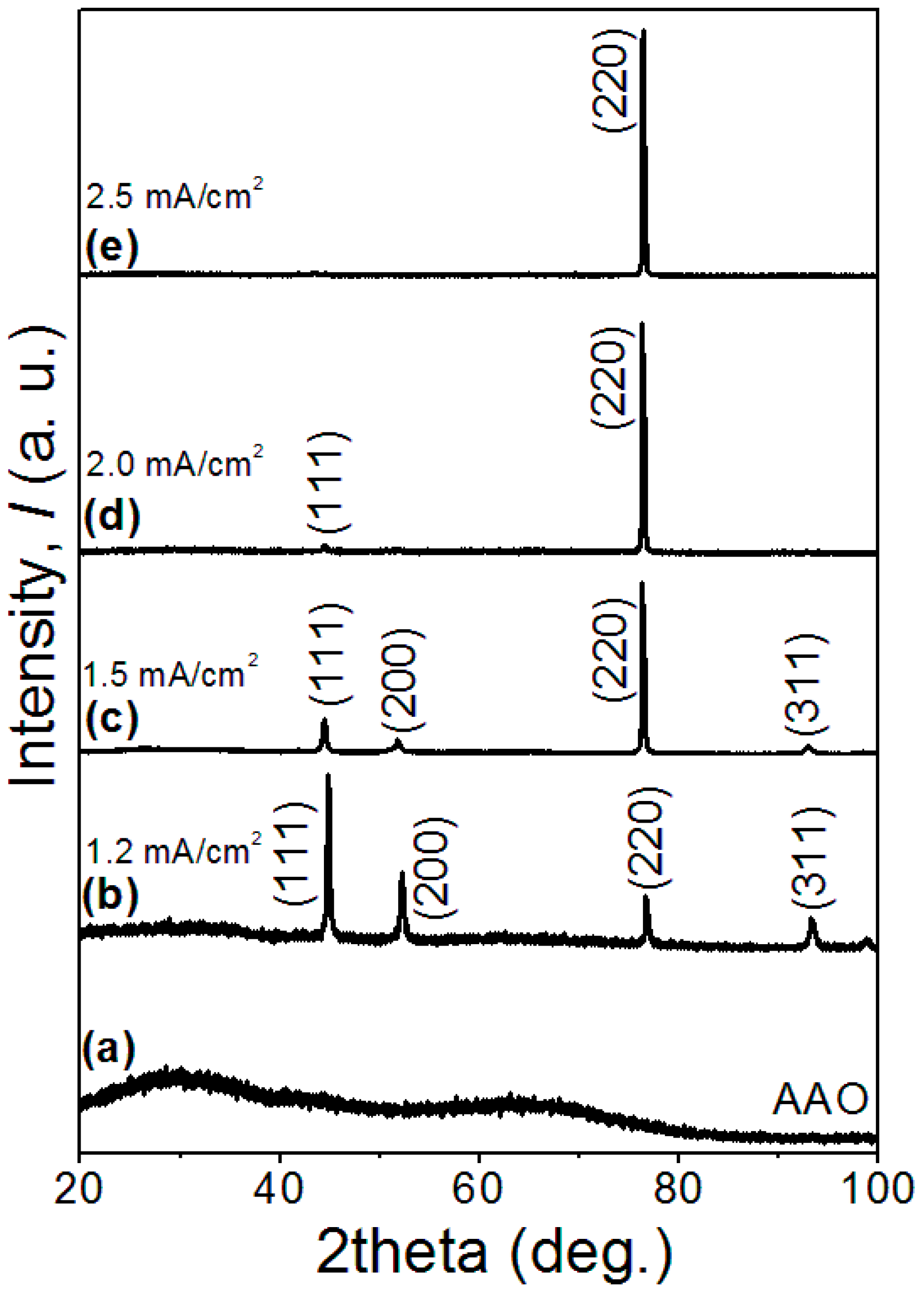
Abstract
:1. Introduction
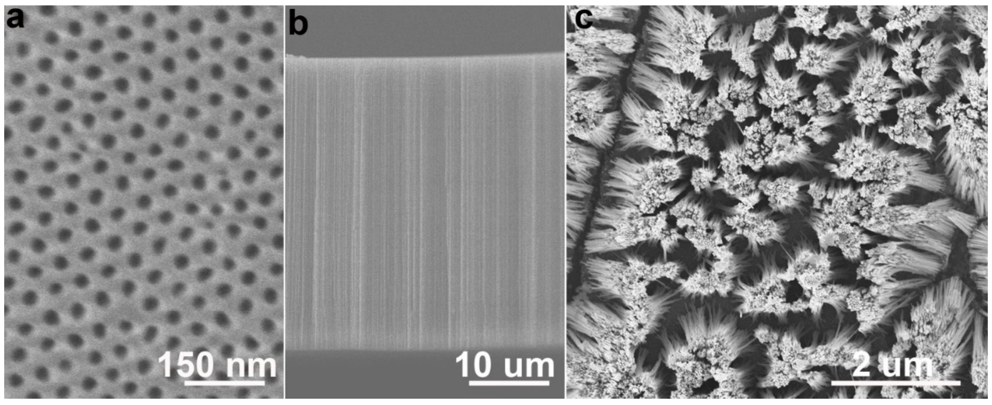
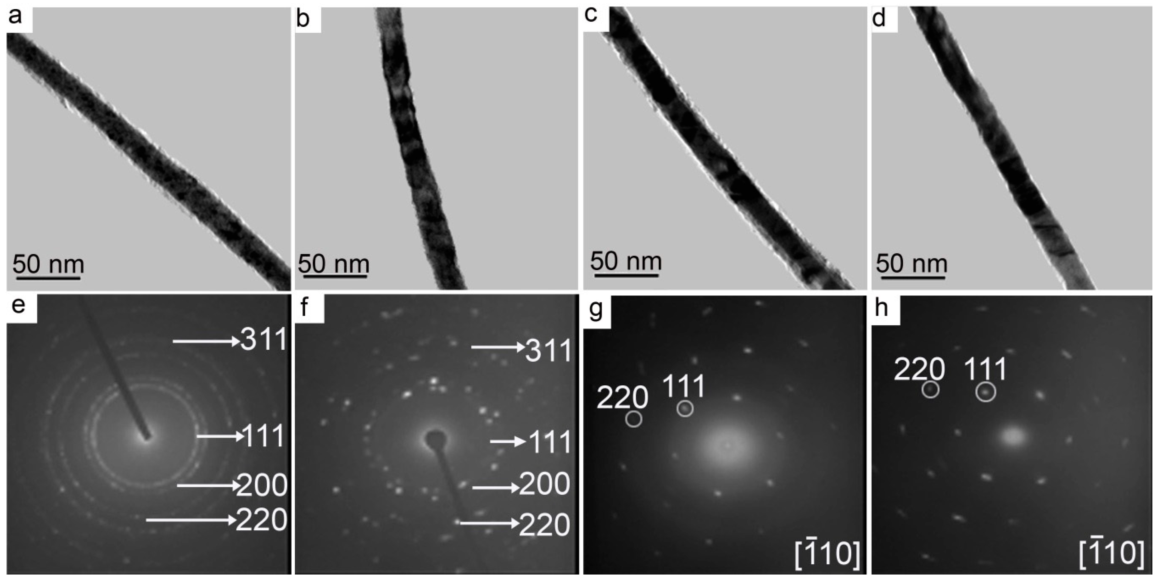
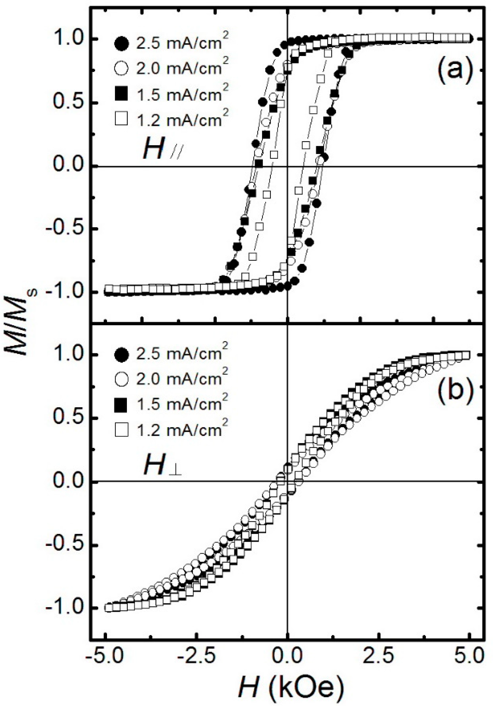
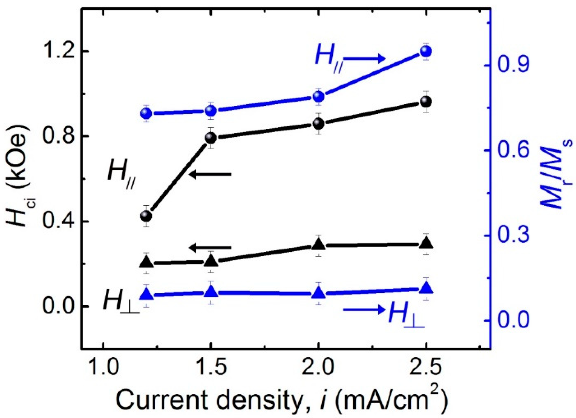
2. Results and Discussion
3. Experimental
3.1. Fabrication of AAO Template
3.2. Electrodeposition of Ni Nanowire Arrays
3.3. Materials Characterization
4. Conclusions
Funding
Conflicts of Interest
References
- Parkin, S.S.P.; Hayashi, M.; Thomas, L. Magnetic domain-wall racetrack memory. Science 2008, 320, 190–194. [Google Scholar] [CrossRef] [PubMed]
- Allwood, D.A.; Xiong, G.; Faulkner, C.C.; Atkinson, D.; Petit, D.; Cowburn, R.P. Magnetic domain-wall logic. Science 2005, 309, 1688–1692. [Google Scholar] [CrossRef] [PubMed]
- Catalan, G.; Seidel, J.; Ramesh, R.; Scott, J.F. Domain wall nanoelectronics. Rev. Mod. Phys. 2012, 84, 119–156. [Google Scholar] [CrossRef] [Green Version]
- Belashchenko, K.D.; Tchernyshyov, O.; Kovalev, A.A.; Tretiakov, O.A. Magnetoelectric domain wall dynamics and its implications for magnetoelectric memory. Appl. Phys. Lett. 2016, 108, 132403. [Google Scholar] [CrossRef] [Green Version]
- Garg, C.; Yang, S.-H.; Phung, T.; Pushp, A.; Parkin, S.S.P. Dramatic influence of curvature of nanowire on chiral domain wall velocity. Sci. Adv. 2017, 3, e1602804. [Google Scholar] [CrossRef]
- Whitney, T.M.; Searson, P.C.; Jiang, J.S.; Chien, C.L. Fabrication and magnetic properties of arrays of metallic nanowires. Science 1993, 261, 1316–1319. [Google Scholar] [CrossRef]
- Ivanov, Y.P.; Chuvilin, A.; Lopatin, S.; Kosel, J. Modulated magnetic nanowires for controlling domain wall motion: toward 3D magnetic memories. ACS Nano 2016, 10, 5326–5332. [Google Scholar] [CrossRef]
- Grutter, A.J.; Krycka, K.L.; Tartakovskaya, E.V.; Borchers, J.A.; Reddy, K.S.M.; Ortega, E.; Ponce, A.; Stadler, B.J.H. Complex three-dimensional magnetic ordering in segmented nanowire arrays. ACS Nano 2017, 11, 8311–8319. [Google Scholar] [CrossRef]
- Za’bah, N.F.; Kwa, K.S.K.; Bowen, L.; Mendis, B.; O’Neill, A. Top-down fabrication of single crystal silicon nanowire using optical lithography. J. Appl. Phys. 2012, 112, 024309. [Google Scholar] [CrossRef]
- Min, S.-Y.; Kim, T.-S.; Kim, B.J.; Cho, H.; Noh, Y.-Y.; Yang, H.; Cho, J.H.; Lee, T.-W. Large-scale organic nanowire lithography and electronics. Nat. Commun. 2013, 4, 1773. [Google Scholar] [CrossRef] [Green Version]
- Ozel, T.; Bourret, G.R.; Mirkin, C.A. Coaxial lithography. Nat. Nanotechnol. 2015, 10, 319–324. [Google Scholar] [CrossRef] [PubMed]
- Jin, C.G.; Jiang, G.W.; Liu, W.F.; Cai, W.L.; Yao, L.Z.; Yao, Z.; Li, X.G. Fabrication of large-area single crystal bismuth nanowire arrays. J. Mater. Chem. 2003, 13, 1743. [Google Scholar] [CrossRef]
- Wildt, B.; Mali, A.P.; Searson, P.C. Electrochemical template synthesis of multisegment nanowires: fabrication and protein functionalization. Langmuir 2006, 22, 10528–10534. [Google Scholar] [CrossRef] [PubMed]
- Pan, H.; Liu, B.; Yi, J.; Poh, C.; Lim, S.; Ding, J.; Feng, Y.; Huan, C.H.A.; Lin, J. Growth of single-crystalline Ni and Co nanowires via electrochemical deposition and their magnetic properties. J. Phys. Chem. B 2005, 109, 3094–3098. [Google Scholar] [CrossRef]
- Han, X.-F.; Shamaila, S.; Sharif, R.; Chen, J.-Y.; Liu, H.-R.; Liu, D.-P. Structural and magnetic properties of various ferromagnetic nanotubes. Adv. Mater. 2009, 21, 4619–4624. [Google Scholar]
- Yue, G.; Xu, Q.; Meng, G.; He, X.; Han, F.; Zhang, L. Electrochemical synthesis and magnetic properties of single-crystal and netlike poly-crystal Ni nanowire arrays. J. Alloys Compd. 2009, 477, L30–L34. [Google Scholar] [CrossRef]
- Medina, J.D.; Hamoir, G.; Velázquez-Galván, Y.; Pouget, S.; Okuno, H.; Vila, L.; Encinas, A.; Piraux, L. Large magnetic anisotropy enhancement in size controlled Ni nanowires electrodeposited into nanoporous alumina templates. Nanotechnology 2016, 27, 145702. [Google Scholar] [CrossRef] [PubMed]
- Sun, H.Y.; Yu, Y.L.; Li, X.H.; Li, W.; Li, F.; Liu, B.T.; Zhang, X.Y. Controllable growth of electrodeposited single-crystal nanowire arrays: The examples of metal Ni and semiconductor ZnS. J. Cryst. Growth 2007, 307, 472–476. [Google Scholar] [CrossRef]
- Sun, H.Y.; Li, X.H.; Chen, Y.; Li, W.; Li, F.; Liu, B.T.; Zhang, X.Y. The control of the growth orientations of electrodeposited single-crystal nanowire arrays: a case study for hexagonal CdS. Nanotechnology 2008, 19, 225601. [Google Scholar] [CrossRef]
- Masuda, H.; Fukuda, K. Ordered metal nanohole arrays made by a two-step replication of honeycomb structures of anodic alumina. Science 1995, 268, 1466–1468. [Google Scholar] [CrossRef]
- Li, Z.; Li, Y.; Li, S.; Wu, J.; Hu, X.; Ling, Z.; Jin, L. A modified quantitative method for regularity evaluation of porous AAO and related intrinsic mechanisms. J. Electrochem. Soc. 2018, 165, E214–E220. [Google Scholar] [CrossRef]
- Wen, L.; Xu, R.; Mi, Y.; Lei, Y. Multiple nanostructures based on anodized aluminium oxide templates. Nat. Nanotechnol. 2017, 12, 244–250. [Google Scholar] [CrossRef] [PubMed]
- Ashley, M.J.; O’Brien, M.N.; Hedderick, K.R.; Mason, J.A.; Ross, M.B.; Mirkin, C.A. Templated synthesis of uniform perovskite nanowire arrays. J. Am. Chem. Soc. 2016, 138, 10096–10099. [Google Scholar] [CrossRef] [PubMed]
- Xue, J.; Zhou, Z.-K.; Wei, Z.; Su, R.; Lai, J.; Li, J.; Li, C.; Zhang, T.; Wang, X.-H. Scalable, full-colour and controllable chromotropic plasmonic printing. Nat. Commun. 2015, 6, 8906. [Google Scholar] [CrossRef] [PubMed] [Green Version]
- Tan, M.; Chen, X.Q. Growth mechanism of single crystal nanowires of fcc metals (Ag, Cu, Ni) and hcp metal (Co) electrodeposited. J. Electrochem. Soc. 2012, 159, K15–K20. [Google Scholar] [CrossRef]
- Cortés, A.; Riveros, G.; Palma, J.L.; Denardin, J.C.; Marotti, R.E.; Dalchiele, E.A.; Gómez, H. Single-crystal growth of nickel nanowires: influence of deposition conditions on structural and magnetic properties. J. Nanosci. Nanotechnol. 2009, 9, 1992–2000. [Google Scholar] [CrossRef] [PubMed]
- Wang, X.W.; Fei, G.T.; Xu, X.J.; Jin, Z.; Zhang, L.D. Size-dependent orientation growth of large-area ordered Ni nanowire arrays. J. Phys. Chem. B 2005, 109, 24326–24330. [Google Scholar] [CrossRef] [PubMed]
- Wang, X.W.; Fei, G.T.; Chen, L.; Xu, X.J.; Zhang, L.D. Orientation-controllable growth of Ni nanowire arrays with different diameters. Electrochem. Solid-State Lett. 2007, 10, E1–E3. [Google Scholar] [CrossRef]
- Dellis, S.; Christoulaki, A.; Spiliopoulos, N.; Anastassopoulos, D.L.; Vradis, A.A. Electrochemical synthesis of large diameter monocrystalline nickel nanowires in porous alumina membranes. J. Appl. Phys. 2013, 114, 164308. [Google Scholar] [CrossRef]
- Barriga-Castro, E.D.; García, J.; Mendoza-Reséndez, R.; Prida, V.M.; Luna, C. Pseudo-monocrystalline properties of cylindrical nanowires confinedly grown by electrodeposition in nanoporous alumina templates. RSC Adv. 2017, 7, 13817–13826. [Google Scholar] [CrossRef] [Green Version]
- Prida, V.M.; Hernández-Vélez, M.; Cervera, M.; Pirota, K.; Sanz, R.; Navas, D.; Asenjo, A.; Aranda, P.; Ruiz-Hitzky, E.; Batallán, F.; et al. Magnetic behaviour of arrays of Ni nanowires by electrodeposition into self-aligned titania nanotubes. J. Magn. Magn. Mater. 2005, 294, e69–e72. [Google Scholar] [CrossRef]
- Ashby, M.F.; Ferreira, P.J.; Schodek, D.L. Nanomaterials, Nanotechnologies and Design: An Introduction for Engineers and Architects; Butterworth-Heine-Mann: Oxford, UK, 2009; p. 288. [Google Scholar]
- Paunovic, M.; Schlesinger, M. Fundamentals of Electrochemical Deposition, 2nd ed.; Wiley-Interscience: New York, NY, USA, 2006; p. 114. [Google Scholar]
- Wang, Z.L.; Gao, R.P.; Nikoobakht, B.; El-Sayed, M.A. Surface reconstruction of the unstable {110} surface in gold nanorods. J. Phys. Chem. B 2000, 104, 5417–5420. [Google Scholar] [CrossRef]
- Peng, X.; Manna, L.; Yang, W.; Wickham, J.; Scher, E.; Kadavanich, A.; Alivisatos, A.P. Shape control of CdSe nanocrystals. Nature 2000, 404, 59–61. [Google Scholar] [CrossRef] [PubMed]
- Liu, Y.; Huang, Y.C.; Xiao, Z.B.; Reng, X.W. Study of adsorption of hydrogen on Al, Cu, Mg, Ti surfaces in Al alloy melt via first principles calculation. Metals 2017, 7, 21. [Google Scholar] [CrossRef]
- Löber, R.; Hennig, D. Interaction of hydrogen with transition metal fcc (111) surfaces. Phys. Rev. B 1997, 55, 4761. [Google Scholar] [CrossRef]
- Pan, H.; Sun, H.; Poh, C.; Feng, Y.; Lin, J. Single-crystal growth of metallic nanowires with preferred orientation. Nanotechnology 2005, 16, 1559–1564. [Google Scholar] [CrossRef]
- Sun, L.; Hao, Y.; Chien, C.-L.; Searson, P.C. Tuning the properties of magnetic nanowires. IBM J. Res. Dev. 2005, 49, 79–102. [Google Scholar] [CrossRef]
- Yu, C.Y.; Yu, Y.L.; Sun, H.Y.; Xu, T.; Li, X.H.; Li, W.; Gao, Z.S.; Zhang, X.Y. Enhancement of the coercivity of electrodeposited nickel nanowire arrays. Mater. Lett. 2007, 61, 1859–1862. [Google Scholar] [CrossRef]
- Song, Y.; Lu, W.; Xu, Y.; Shi, J.; Fang, X. Growth of single-crystalline Co7Fe3 nanowires via electrochemical deposition and their magnetic properties. J. Alloys Compd. 2015, 652, 179–184. [Google Scholar] [CrossRef]
- Kartopu, G.; Yalçın, O.; Choy, K.-L.; Topkaya, R.; Kazan, S.; Aktaş, B. Size effects and origin of easy-axis in nickel nanowire arrays. J. Appl. Phys. 2011, 109, 033909. [Google Scholar] [CrossRef]
- Chen, C.H.; Knutson, S.J.; Shen, Y.; Wheeler, R.A.; Horwath, J.C.; Barnes, P.N. The effect of particle size on coercivity and crystallinity of SmCo5. Appl. Phys. Lett. 2011, 99, 012504. [Google Scholar] [CrossRef]
- Shaterabadi, Z.; Soltanian, S.; Koohbor, M.; Salimi, A.; Servati, P. Modification of microstructure and magnetic properties of electrodeposited Co nanowire arrays: A study of the effect of external magnetic field, electrolyte acidity and annealing process. Mater. Chem. Phys. 2015, 160, 389–397. [Google Scholar] [CrossRef]
- Chen, Y.; Yan, H.; Li, X.H.; Li, W.; Zhang, J.W.; Zhang, X.Y. Assembly of Ni/γ-Fe2O3 shell/core nanowires. Mater. Lett. 2006, 60, 245–247. [Google Scholar] [CrossRef]
- Sun, H.Y.; Li, X.H.; Li, W.; Li, F.; Liu, B.T.; Zhang, X.Y. Low-temperature synthesis of wurtzite ZnS single-crystal nanowire arrays. Nanotechnology 2007, 18, 115604. [Google Scholar] [CrossRef]


© 2019 by the authors. Licensee MDPI, Basel, Switzerland. This article is an open access article distributed under the terms and conditions of the Creative Commons Attribution (CC BY) license (http://creativecommons.org/licenses/by/4.0/).
Share and Cite
Yu, Y.; Li, J.; Wang, J.; Wu, X.; Yu, C.; Xu, T.; Chang, B.; Sun, H.; Arandiyan, H. Orientation Growth and Magnetic Properties of Electrochemical Deposited Nickel Nanowire Arrays. Catalysts 2019, 9, 152. https://doi.org/10.3390/catal9020152
Yu Y, Li J, Wang J, Wu X, Yu C, Xu T, Chang B, Sun H, Arandiyan H. Orientation Growth and Magnetic Properties of Electrochemical Deposited Nickel Nanowire Arrays. Catalysts. 2019; 9(2):152. https://doi.org/10.3390/catal9020152
Chicago/Turabian StyleYu, Yanlong, Jinpeng Li, Jun Wang, Xige Wu, Cuiyan Yu, Tao Xu, Bingdong Chang, Hongyu Sun, and Hamidreza Arandiyan. 2019. "Orientation Growth and Magnetic Properties of Electrochemical Deposited Nickel Nanowire Arrays" Catalysts 9, no. 2: 152. https://doi.org/10.3390/catal9020152