
Optical Beam Deflection Based AFM with Integrated Hardware and Software Platform for an Undergraduate Engineering Laboratory


Abstract
:
1. Introduction
2. Materials and Methods
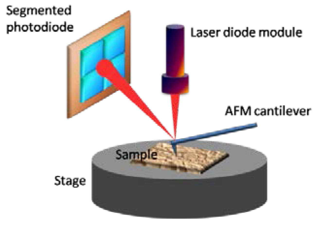
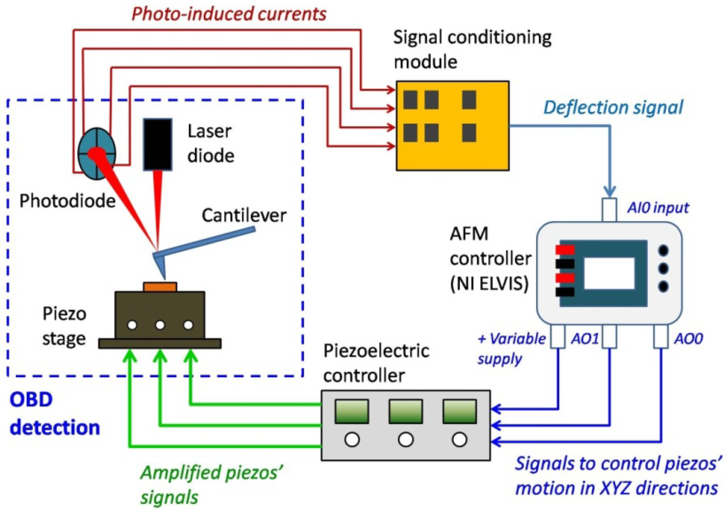
2.1. Optical Beam Deflection (OBD) Detection
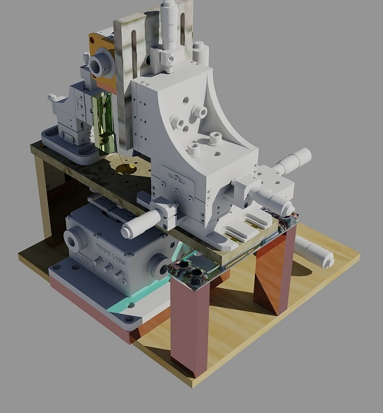
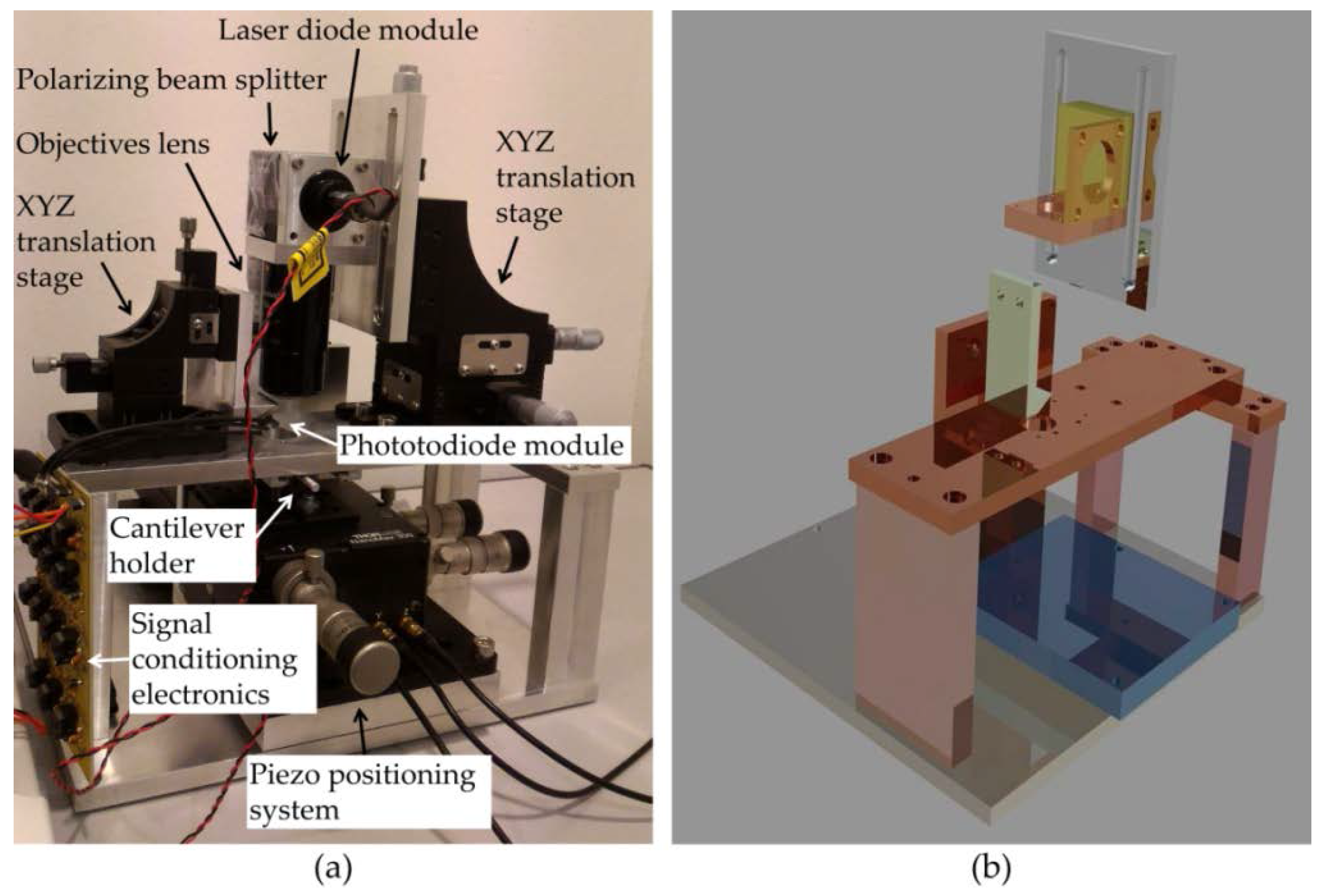
2.2. AFM Setup
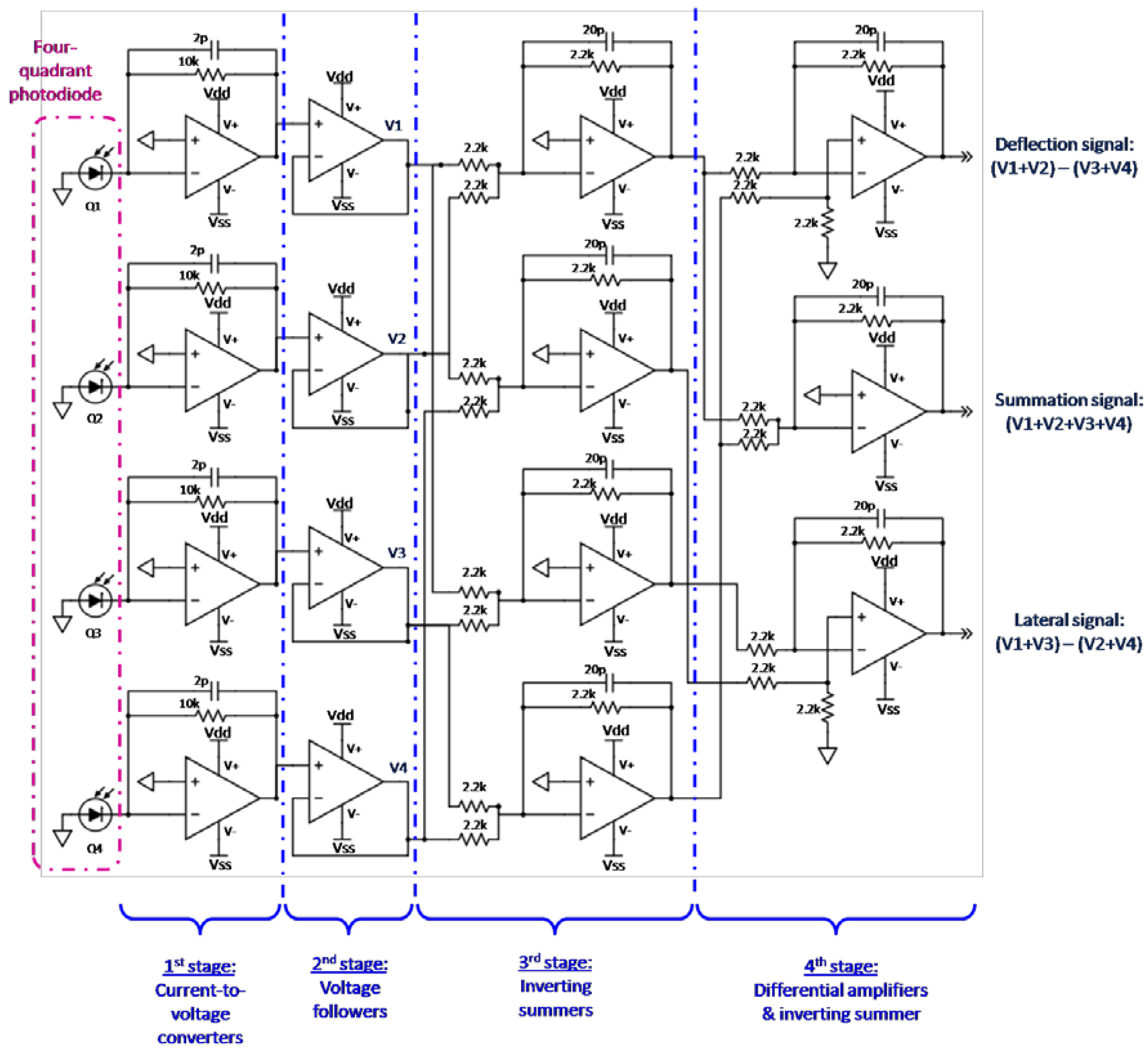
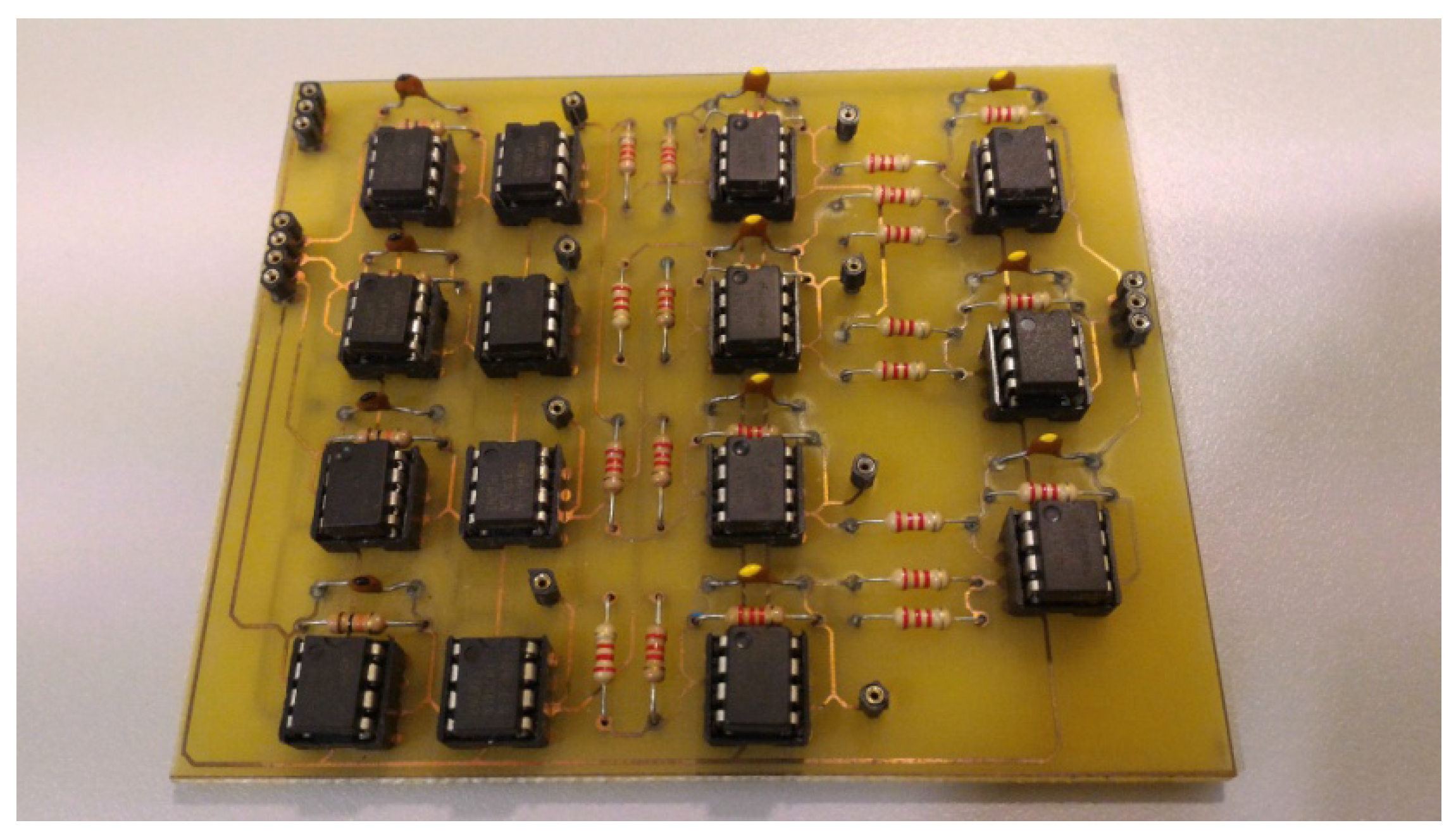
2.3. Electronics
2.4. Controller
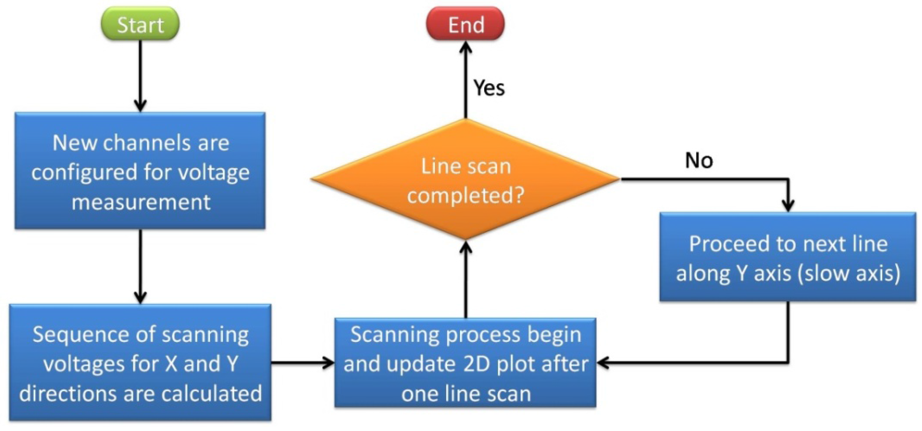
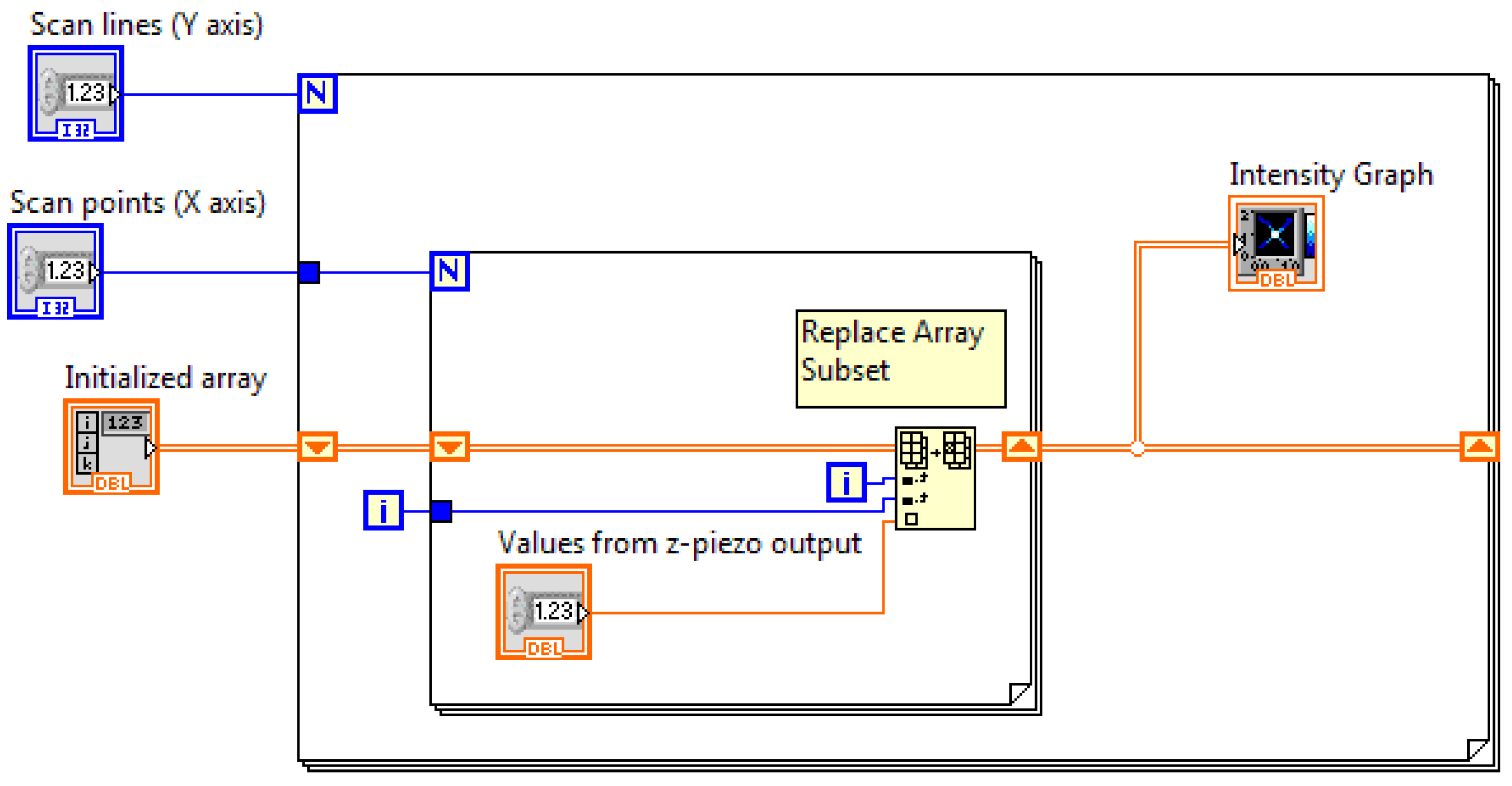
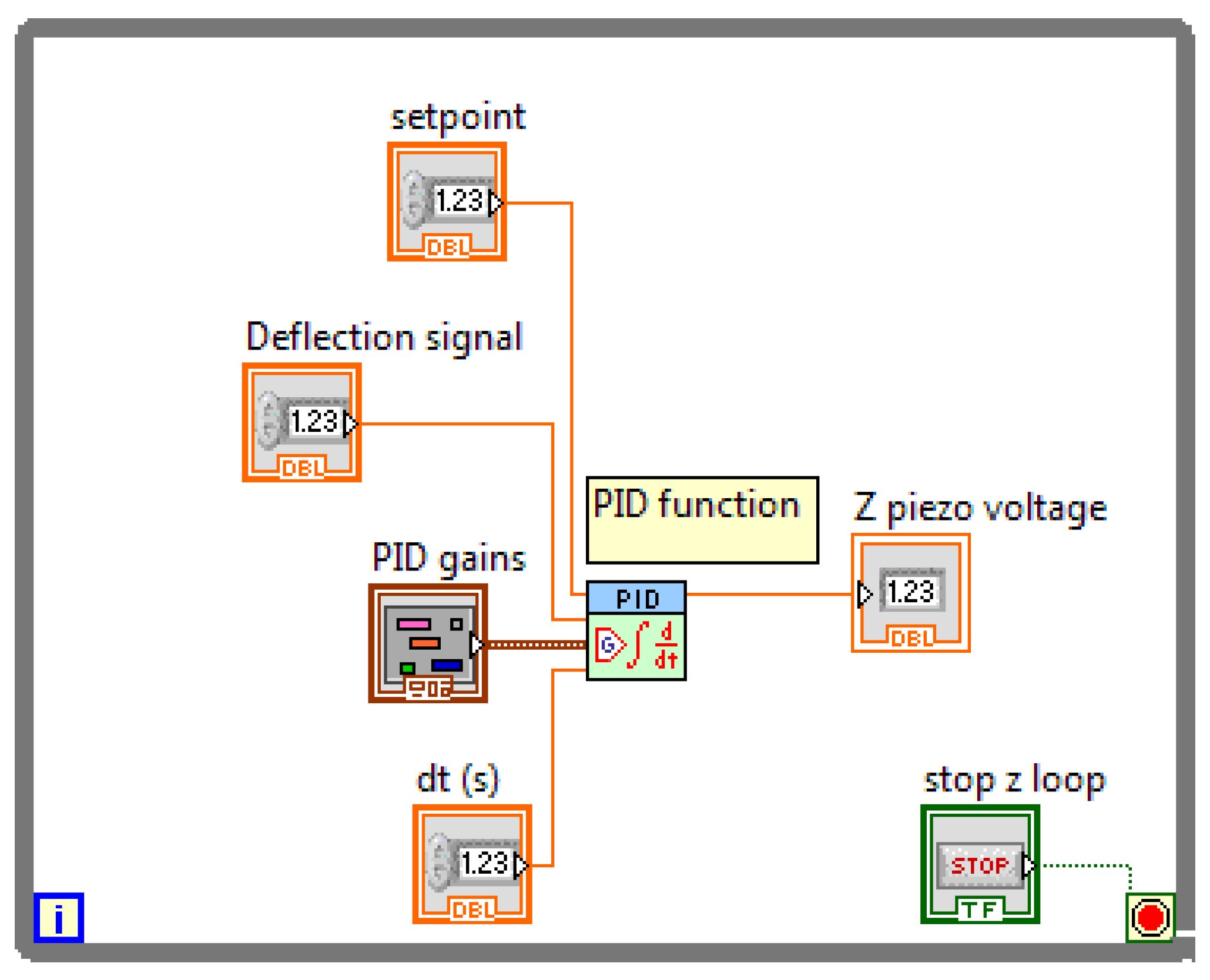
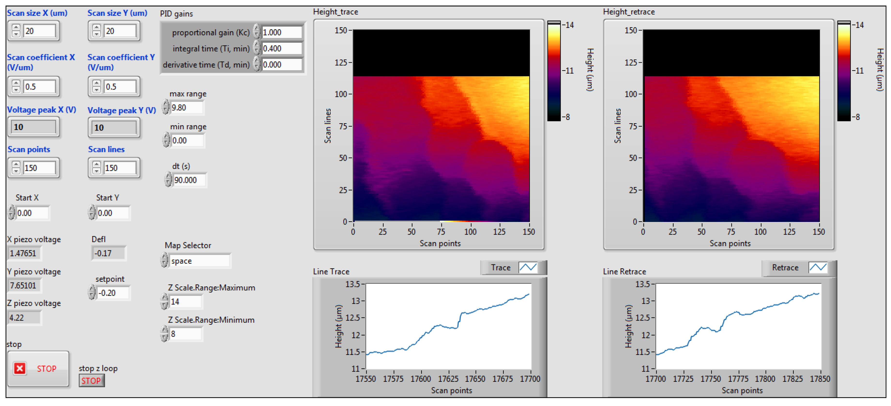
2.5. Software
2.6. Approximate Cost of the System
3. Results and Discussion
3.1. Laser Alignment and Tip Engagement
3.2. Imaging Results
3.3. Limitations and Further Improvements
4. Conclusions
Supplementary Materials
Acknowledgments
Author Contributions
Conflicts of Interest
References
- Binnig, G.; Quate, C.F.; Gerber, C. Atomic Force Microscope. Phys. Rev. Lett. 1986, 56, 930–933. [Google Scholar] [CrossRef] [PubMed]
- Giessibl, F.J. Atomic Resolution of the Silicon (111)-(7×7) Surface by AFM. Science 1995, 267, 68–71. [Google Scholar] [CrossRef] [PubMed]
- Giessibl, F.J. Atomic resolution on Si(111)-(7×7) by noncontact atomic force microscopy with a force sensor based on a quartz tuning fork. Appl. Phys. Lett. 2000, 76, 1470–1472. [Google Scholar] [CrossRef]
- Eguchi, T.; Hasegawa, Y. High Resolution Atomic Force Microscopic Imaging of the Si(111)-(7×7) Surface: Contribution of Short-Range Force to the Images. Phys. Rev. Lett. 2002, 89, 266105. [Google Scholar] [CrossRef] [PubMed]
- Reichling, M.; Huisinga, M.; Gogoll, S.; Barth, C. Degradation of the CaF2(111) surface by air exposure. Surf. Sci. 1999, 439, 181–190. [Google Scholar] [CrossRef]
- Reichling, M.; Barth, C. Scanning Force Imaging of Atomic Size Defects on the CaF2(111) Surface. Phys. Rev. Lett. 1999, 83, 768–771. [Google Scholar] [CrossRef]
- Barth, C.; Reichling, M. Imaging the atomic arrangements on the high-temperature reconstructed α-Al2O3(0001) surface. Nature 2001, 414, 54–57. [Google Scholar] [CrossRef] [PubMed]
- Enevoldsen, G.H.; Foster, A.S.; Christensen, M.C.; Lauritsen, J.V.; Besenbacher, F. Noncontact atomic force microscopy studies of vacancies and hydroxyls of TiO2(110): Experiments and atomistic simulations. Phys. Rev. B 2007, 76, 205415. [Google Scholar] [CrossRef]
- Loh, S.H.; Jarvis, S.P. Visualization of Ion Distribution at the Mica-Electrolyte Interface. Langmuir 2010, 26, 9176–9178. [Google Scholar] [CrossRef] [PubMed]
- Kilpatrick, J.I.; Loh, S.H.; Jarvis, S.P. Directly Probing the Effects of Ions on Hydration Forces at Interfaces. J. Am. Chem. Soc. 2013, 135, 2628–2634. [Google Scholar] [CrossRef] [PubMed]
- Voigtländer, B. Scanning Probe Microscopy: Atomic Force Microscopy and Scanning Tunneling Microscopy; Springer: Berlin/Heidelberg, Germany, 2015. [Google Scholar]
- Bhushan, B.; Marti, O. Scanning Probe Microscopy—Principle of Operation, Instrumentation, and Probes. In Springer Handbook of Nanotechnology; Bhushan, B., Ed.; Springer: Berlin/Heidelberg, Germany, 2004; pp. 325–369. [Google Scholar]
- Sarid, D. Scanning Force Microscopy with Applications to Electric, Magnetic, and Atomic Forces; Oxford University Press: New York, NY, USA, 1994. [Google Scholar]
- Greczyło, T.; Debowska, E. The macroscopic model of an atomic force microscope in the students’ laboratory. Eur. J. Phys. 2006, 27, 501–513. [Google Scholar] [CrossRef]
- Planinšič, G.; Kovač, J. Nano goes to school: A teaching model of the atomic force microscope. Phys. Educ. 2008, 43, 37–45. [Google Scholar] [CrossRef]
- Bonson, K.; Headrick, R.L.; Hammond, D.; Hamblin, M. Working model of an atomic force microscope. Am. J. Phys. 2011, 79, 189–192. [Google Scholar] [CrossRef]
- Hsieh, T.H.; Tsai, Y.C.; Kao, C.J.; Chang, Y.M.; Lu, Y.W. A conceptual atomic force microscope using LEGO for nanoscience education. Int. J. Autom. Smart Technol. 2014, 4, 113–121. [Google Scholar]
- Shusteff, M.; Burg, T.P.; Manalis, S.R. Measuring Boltzmann’s constant with a low-cost atomic force microscope: An undergraduate experiment. Am. J. Phys. 2006, 74, 873–879. [Google Scholar] [CrossRef]
- Bergmann, A.; Feigl, D.; Kuhn, D.; Schaupp, M.; Quast, G.; Busch, K.; Eichner, L.; Schumacher, J. A low-cost AFM setup with an interferometer for undergraduates and secondary-school students. Eur. J. Phys. 2013, 34, 901–914. [Google Scholar] [CrossRef]
- Jones, C.N.; Gonçalves, J. A cost-effective atomic force microscope for undergraduate control laboratories. IEEE Trans. Educ. 2010, 53, 328–334. [Google Scholar] [CrossRef]
- Meyer, G.; Amer, N.M. Novel optical approach to atomic force microscopy. Appl. Phys. Lett. 1988, 53, 1045–1047. [Google Scholar] [CrossRef]
- Cheah, W.J.; Loh, S.H. Design of electronic module for OBD system in AFM for undergraduate study. In Proceedings of the 6th IEEE International Conference on Control System, Computing and Engineering (ICCSCE 2016), Penang, Malaysia, 25–27 November 2016; pp. 33–38.


| Item | Cost |
|---|---|
| Personal computer | $500 |
| NI ELVIS | $4000 |
| Piezo positioning system | $3800 |
| Optical components | $900 |
| XYZ manual translation stages | $2500 |
| Custom-built mechanical parts | $500 |
| Signal conditioning electronics and photodiode | $100 |
| Total | $12,300 |
© 2017 by the authors. Licensee MDPI, Basel, Switzerland. This article is an open access article distributed under the terms and conditions of the Creative Commons Attribution (CC BY) license ( http://creativecommons.org/licenses/by/4.0/).
Share and Cite
Loh, S.H.; Cheah, W.J. Optical Beam Deflection Based AFM with Integrated Hardware and Software Platform for an Undergraduate Engineering Laboratory. Appl. Sci. 2017, 7, 226. https://doi.org/10.3390/app7030226
Loh SH, Cheah WJ. Optical Beam Deflection Based AFM with Integrated Hardware and Software Platform for an Undergraduate Engineering Laboratory. Applied Sciences. 2017; 7(3):226. https://doi.org/10.3390/app7030226
Chicago/Turabian StyleLoh, Siu Hong, and Wei Jie Cheah. 2017. "Optical Beam Deflection Based AFM with Integrated Hardware and Software Platform for an Undergraduate Engineering Laboratory" Applied Sciences 7, no. 3: 226. https://doi.org/10.3390/app7030226