


Energy Efficient Enhancement in a 5.8 GHz Batteryless Node Suitable for Backscattering Communications

Department of Information Engineering, University of Florence, V. S. Marta, 3, 50139 Florence, Italy
*
Author to whom correspondence should be addressed.
Electronics 2023, 12(10), 2256; https://doi.org/10.3390/electronics12102256
Submission received: 11 April 2023
/
Revised: 11 May 2023
/
Accepted: 13 May 2023
/
Published: 16 May 2023
(This article belongs to the Special Issue Energy Harvesting and Energy Storage Systems, Volume II)
Abstract
:This work presents a compact batteryless node architecture suitable with the backscattering communication (BackCom) approach. The key functional blocks are demonstrated at 5.8 GHz, making use of commercially available components involving a DC/DC step-up converter, a 3.3 V data generator, and an ASK backscattering modulator based on a single GaAs HEMT in a cold-FET configuration. The node integrates a patch antenna exhibiting a non-50 optimal port impedance; the value is defined by means of a source pull-based optimization technique aimed at maximizing the DC/DC input current supplied by the RF to DC converter. This approach maximizes the node compactness, as well as the wireless power conversion efficiency. A prototype was optimized for the −5 dBm power level at the input of the RF to DC converter. Under this measurement condition, the experimental results showed a 63% increase in the harvesting current, rising from 145 to 237 A, compared to an identical configuration that used a microstrip matching network coupled with a typical 50- patch antenna. In terms of harvested power, the achieved improvement was from −13.2 dBm to −10.9 dBm. The conversion efficiency in an operative condition improved from 15% to more than 25%. In this condition, the node is capable of charging a 100 F to the operative voltage in about 27 s, and operating the backscattering for 360 ms with a backscattering modulation frequency of about 10 MHz.
1. Introduction
In recent years, there has been a growing interest in exploiting the Internet of Things (IoT) paradigms in many contexts, such as the control of processes in assisted ambient intelligent [1], industrial environments [2], and environmental quality [3]. A major factor that has fostered the development of IoT on a large scale is the projected growth in distributed communications and computing technologies [4,5]. The application of these technologies has led to IoT technologies fulfilling some key requirements, including low energy consumption [6,7,8] and, possibly, the development of hardware nodes that feature small batteries (or that even operate without batteries). As a consequence, a number of approaches aimed at overcoming this problem were envisioned in the last few years, including technical solutions such as the concepts of energy harvesting (EH) and wireless power transfer (WPT) [9]. These are complemented by new technical concepts aimed at sustaining the coexistence of a large number of wireless devices for IoT applications (with the drawback of reduced battery life). In order to overcome (or at least minimize) these limitations, one of the most promising solutions is the so-called backscattering communication (BackCom) technique [10,11,12]. This approach is based on the controlled reflection of the electromagnetic wave that incorporates the data to be forwarded to the receiving node. It can be easily demonstrated that not having any carrier source on board to reflect the IoT node allows for transmitting forward data while minimizing energy consumption. Furthermore, in the BackCom vision, communication is obtained by avoiding the implementation of most of the functional blocks in the transmitting/receiving chain (i.e., oscillators, mixers), reducing device complexity, and decreasing production costs [13,14]. Additionally, such node architectures usually involve EH and/or WPT to fully overcome the energy constraints and extend the battery life, as illustrated in [15,16,17].
A primitive example of BackCom design principles can be observed in the use of radio-frequency identification (RFID) technology [18] in vehicular communications. Nonetheless, the expected performance associated with a batteryless BackCom-based IoT node requires communication capabilities and ranges that surpass those of a typical RFID device scenario. Following this, the final step in improving the feasibility of IoT paradigms, with respect to power limitations, is the development of fully batteryless BackCom nodes that implement specific solutions supporting both burst and low-rate operations [19].
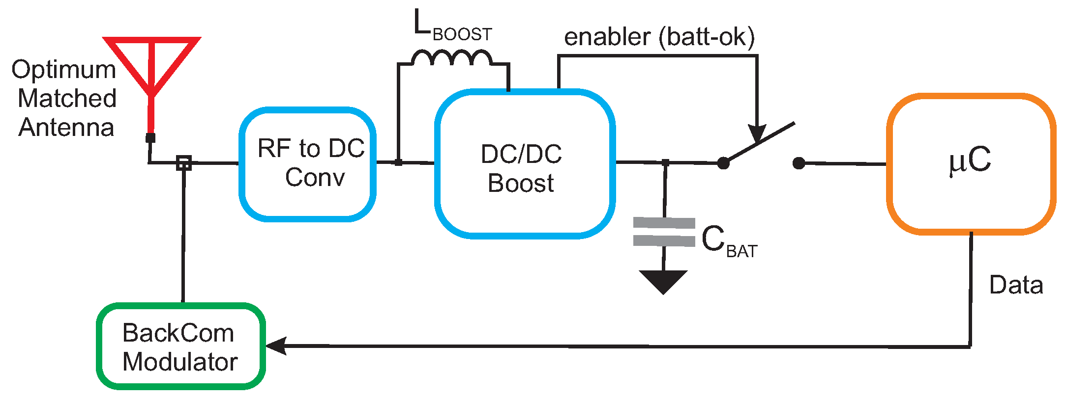
In this paper, the authors demonstrate the feasibility of a simple yet fully compliant batteryless BackCom node system that is compatible with the implementation of IoT network architectures. The node has been demonstrated at 5.8 GHz, making use of component-off-the-shelf (COTS) devices. The latter includes a harvester block that is based on a rectifier driving a DC/DC boost, as well as a modulator block, which is controlled by a microcontroller included in the node’s prototype. Moreover, the proposed BackCom node system integrates a patch antenna, showing a non-50- optimal port impedance. The proposed node system architecture, illustrated in Figure 1, was developed by following an approach that is fully compatible with frequency scalability and with an integrated design based on the standard IC process.
The paper, in addition to the introduction, is organized into three further sections. The next section is dedicated to the description of the proposed node architecture, including the harvester, the modulator, and the antenna. The third section presents a discussion of the prototype’s system-level architecture, while the fourth section describes the performance; the final section presents the conclusive discussion.
2. The BackCom Node Key’s Functional Blocks
The batteryless node architecture was designed to be compliant with the operation principle of the BackCom approach, and consists of the following three functional blocks: the harvester, the modulator, and the antenna (Figure 1).
The operational sequence of the proposed node can be summarized as follows:
- Firstly, the base station queries the node and supplies it with a continuous wave RF signal at 5.8 GHz;
- Secondly, the RF to DC converter and the DC/DC boost harvest the received RF energy and charge the ;
- Thirdly, when reaches the desired level, , the harvester enables the microcontroller, which controls the backscattering modulator through a GPIO pin;
- Finally, under the control of the microcontroller, the modulator backscatters the RF continuous signal by transmitting the data.
A key feature of the proposed architecture consists of the antenna, which exhibits an internal impedance capable of optimizing the RF to DC energy conversion by maximizing the current provided to the DC–DC converter; the impedance of the antenna is estimated using a source pull-based technique. This in turn maximizes the wireless power conversion efficiency of the harvester block [20,21], and permits the inclusion of commercial DC–DC converters.
From an operational point of view, the architecture increases the operational time window suitable for backscattering communication, minimizing the energy harvesting time.
The following subsections illustrate the characteristics of the aforementioned functional blocks.
2.1. RF Energy Harvester
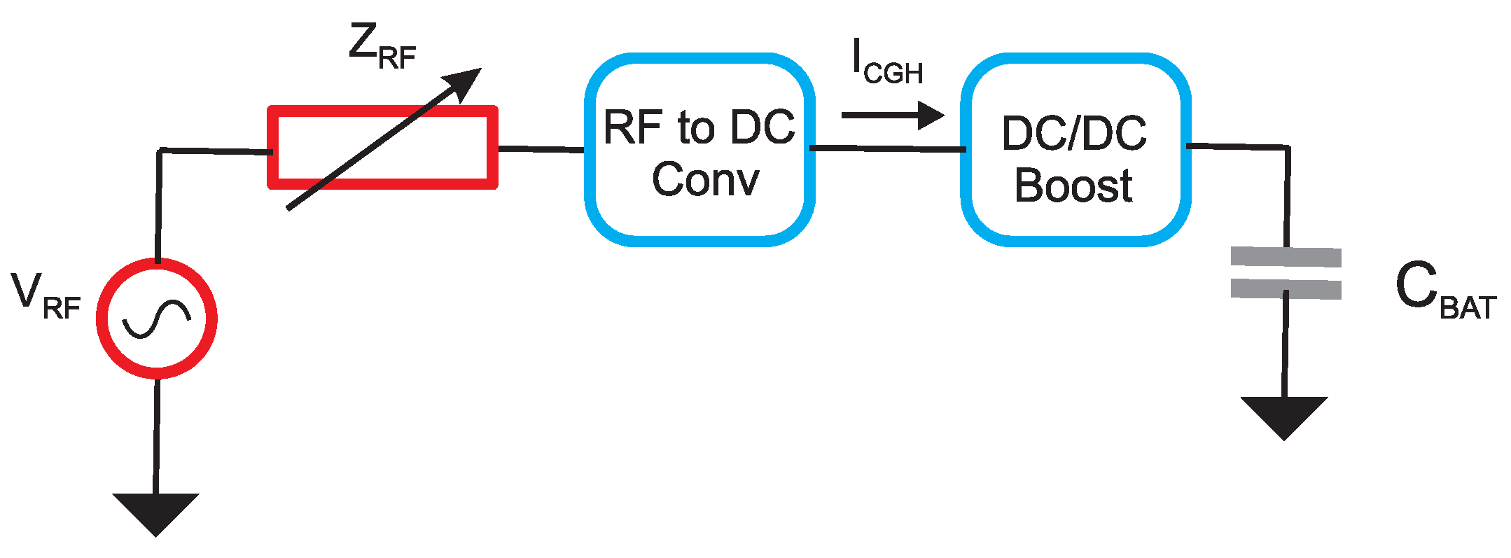
The RF energy harvester block was developed following the approach introduced in [20], and widely discussed and exploited in [21]. The latter makes use of an RF to DC converter based on a voltage multiplier, working on a specific input impedance aimed at maximizing the performance, as well as a commercial nanopower DC/DC boost [22]. Since the harvesting interval sets a lower limit on the querying time, the harvester has to exhibit maximum conversion efficiency during this interval. Based on the previously proposed solution, this objective is obtained by terminating the RF to DC converter with an optimum input impedance. Following [21], the latter consists of the impedance that maximizes the (Figure 1), with respect to the RF input power at the RF to DC converter. To optimize performance for low impinging power, the RF input reference level at the RF to DC converter was set to −5 dBm. Taking into account this power level, and due to the inherently non-linear behavior of the RF to DC converter, a source pull-based optimization was carried out to identify the optimum impedance that the antenna should exhibit to the RF to DC converter. This was obtained by varying , which is the impedance shown by the equivalent RF source, , at the RF to DC converter, as illustrated in Figure 2. In this work, the RF to DC converter was implemented by a diode-based voltage tripler configuration.
Regarding the DC/DC boost, the input port can be described by a behavioral model based on an ideal diode with a threshold voltage . On this basis, the charging current is
where is 0.34 V, in accordance with the experimental results [20], and on the base of manufacturer specifications [22]. Parameters and represent, respectively, the output voltage and the output impedance shown by the RF to DC rectifier toward the DC/DC step-up converter.
The value of the optimum impedance is calculated using the previously described approach by using a source pull-based procedure on a commercial CAD for the high-frequency circuit analysis. This technique consists of running a non-linear analysis at 5.8 GHz with a reference input power of −5 dBm, spanning the source impedance across the entire Smith chart; the target is the impedance that maximizes . In this work, we adopted the zero bias SMS7630-061 Schottky diode in a voltage tripler configuration on silicon; as a result of the source pull-based procedure, the value represents the optimum source impedance. As a consequence, is the impedance to which the harvester input should be terminated during the charging interval; this allows for maximizing the performance and minimizing the latency time between the start of the query and the response of the node.
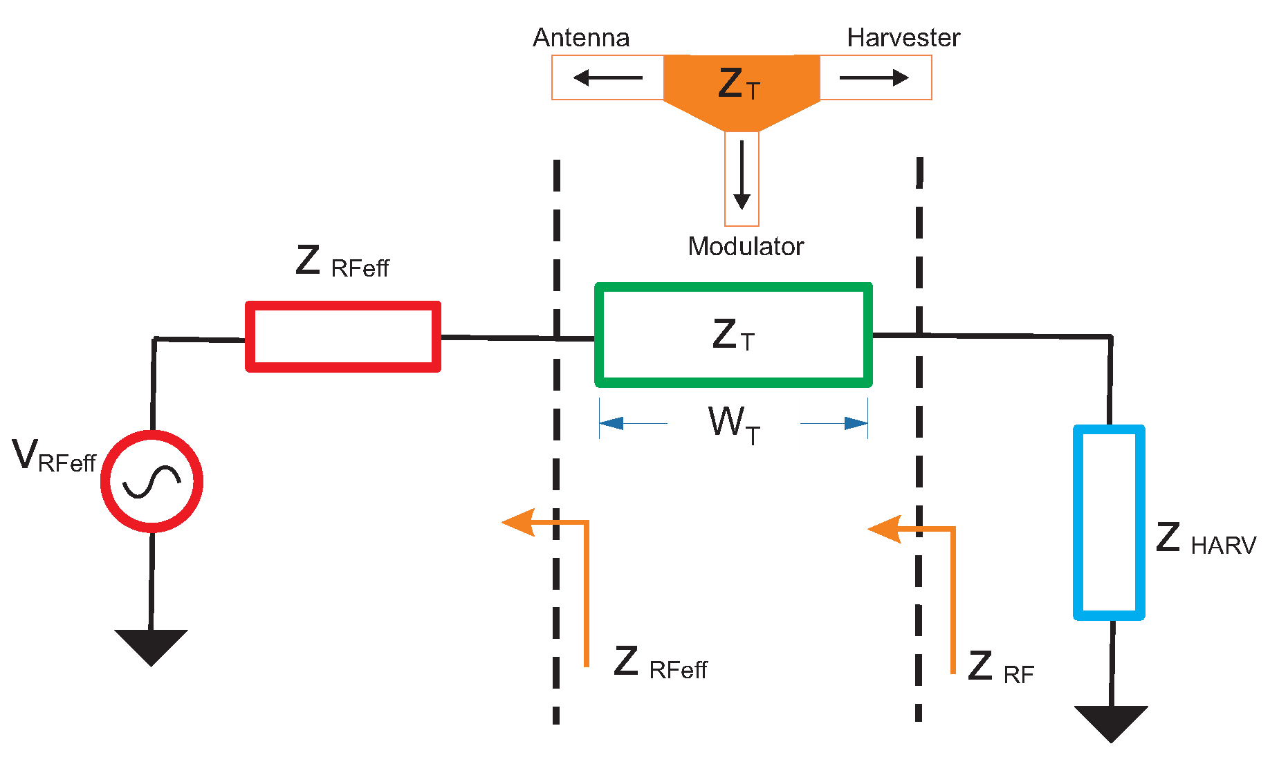
In the present architecture, in order to reduce losses and maximize the compactness of the node, the impedance matching of the voltage tripler is obtained following the approach described in [23]. However, in a BackCom node architecture (Figure 1), the presence of the modulator block cannot be neglected in the harvesting phase (modulator in high impedance state). As a consequence, the identified optimum matching impedance differs from the design impedance that is exhibited by the antenna . The effect of the modulator can be considered by modeling it as a microstrip line with a characteristic impedance and a length , as illustrated in Figure 3.
The values of both and were calculated, starting from the dimensions of the modulator interconnection (the proposed modulator based on a cold-FET configuration, as explained in the specific subsection) between the antenna and the tripler. It is assumed that the modulator exhibits a high impedance at this junction during the harvesting; thus, the can be simply evaluated on the basis of the well-known transmission line equation and the and values.
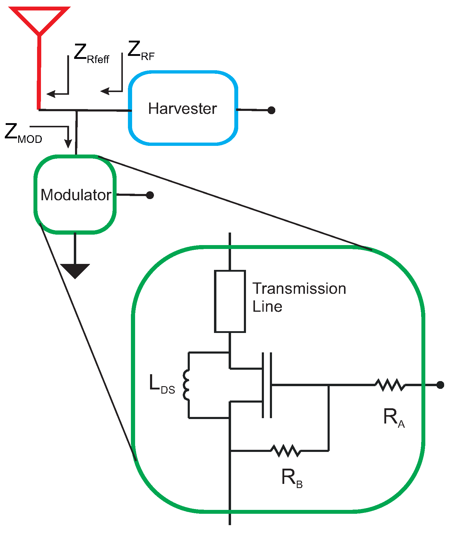
2.2. Modulator
The architecture proposed in this paper for implementing the BackCom node utilizes backscattering modulation, which is a well-known approach for low-power communication [24]. Basically, the backscatterer reflects the impinging radio signal while superimposing a modulation; this feature is obtained by varying the reflection coefficient seen by the antenna. In some approaches, the BackCom node may differentiate the energy and communication paths. This technique simplifies the design of the communication chain by implementing one or two antennas or even two different frequencies. On the contrary, the batteryless BackCom node proposed in the present paper follows a single-path approach for both harvesting and communication. As a consequence, the design procedure has to take into account the use of a single antenna for both harvesting and backscattering.
This approach improves the compactness of the system but it introduces some critical issues in the design process. In particular, the modulator stage has to fulfill two different requirements that are not easily achievable simultaneously. Firstly, the modulator has to satisfy the required modulation parameters; in addition, it has to introduce the minimum effects on power delivery during the harvesting phase.
The topology of the implemented modulator is illustrated in Figure 4. It consists of a cold-FET that is driven by the data output of the microcontroller. The microcontroller was chosen to ensure a significant differentiation between the OFF and ON states of the switch at the operative frequency, regardless of other considerations, such as the settling time of the switch. In addition, because the modulator needs to be carefully designed to ensure proper impedance ( in Figure 5), an accurate model of the device is necessary (which is typically not available at this frequency in other technologies such as CMOS). The cold-FET is connected to the antenna and the harvester by means of a microstrip line, whose length l and width w must be chosen to fulfill the conditions described in (3)
In our design, = , while = . Condition (3) ensures that during the harvesting interval, when the modulator is in a high impedance state, the input power is transferred to the harvester stage, minimizing any losses [21].
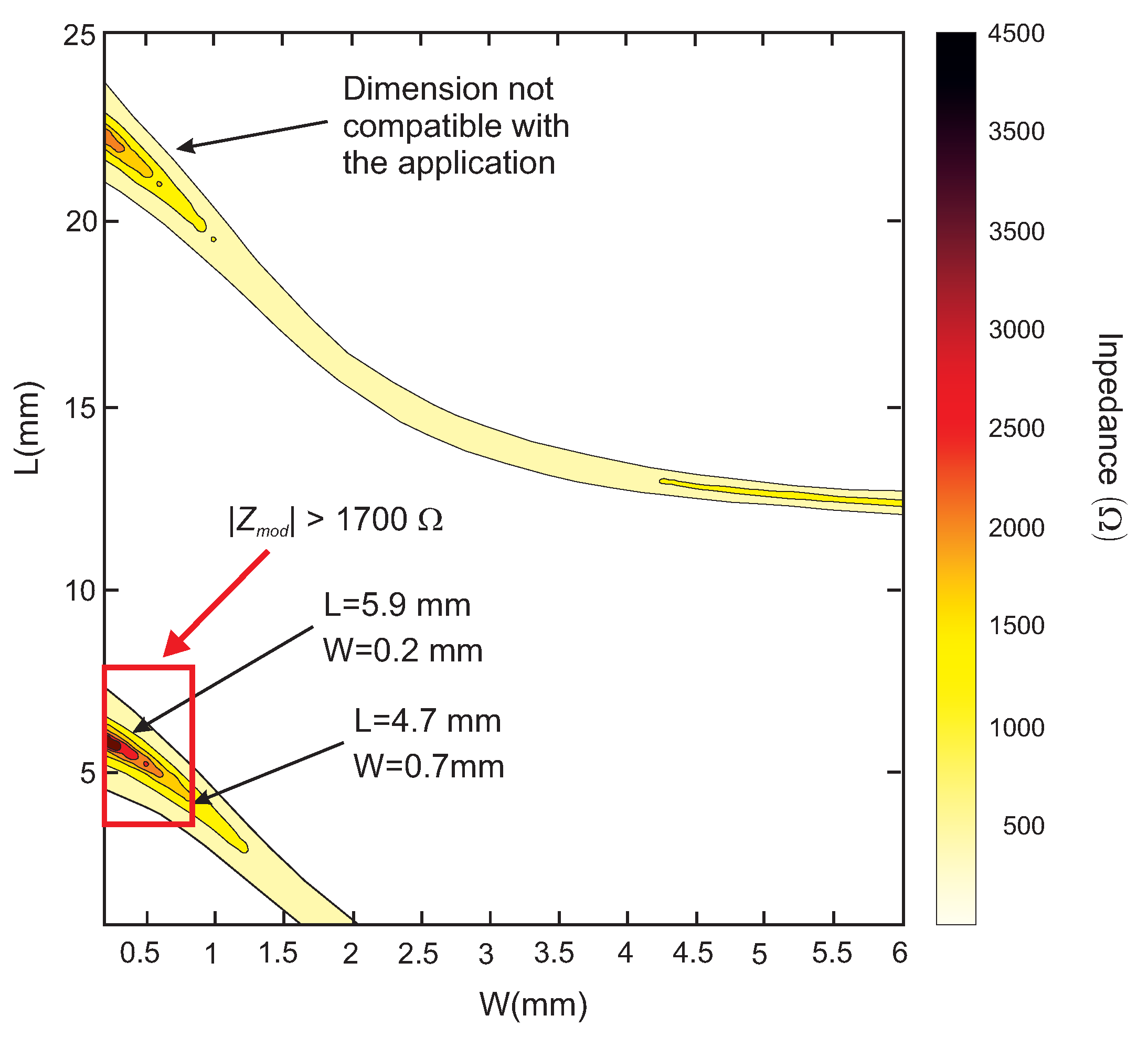
The length l and width w of the microstrip feeding line of the backscattering modulator were chosen after simulating modulator impedance in a high impedance state; the results are depicted in Figure 5.
The dimensions of the modulator feeding line fulfill the conditions of the maximum power transfer given by (3) and maximum compactness. Specifically, the resulting optimal values are mm and mm. These values lead to mm and ; thus, according to (2), the value of the optimum antenna impedance is .
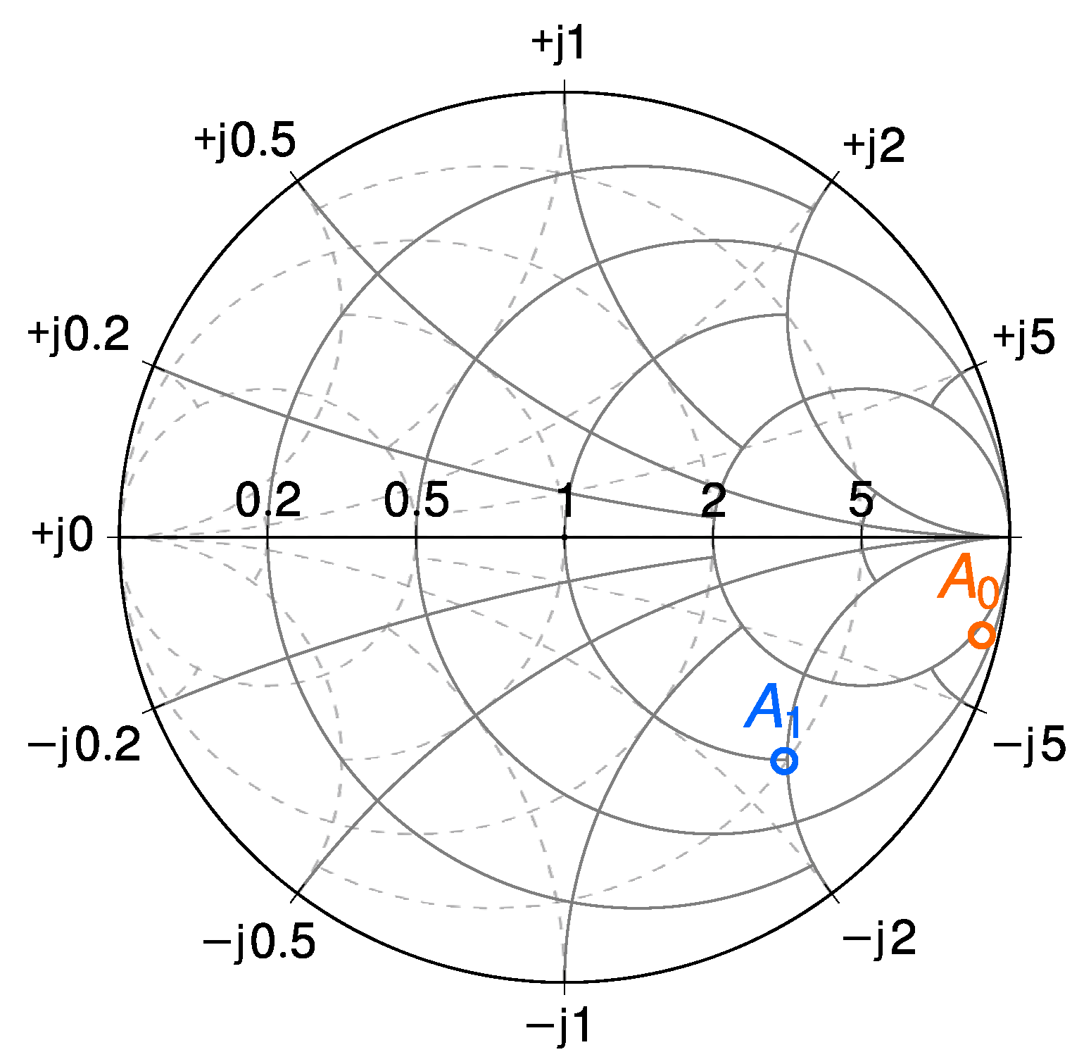
As detailed in [21], the expected ASK modulation depth for a two-symbol modulation is defined as
where each is the simulated reflection coefficient at the antenna port related to the i-th symbol state of the modulator. Through simulations, using the optimal dimensioning of the modulator feed line, the reflection coefficient results, respectively, in = 0.352, = 213 degrees for , = 0.968, and = 347 degrees for , as illustrated in Figure 6, where the two symbols are depicted in the Smith chart. Moreover, from Equation (4), the expected value of the modulation depth is = 0.60.
2.3. Antenna
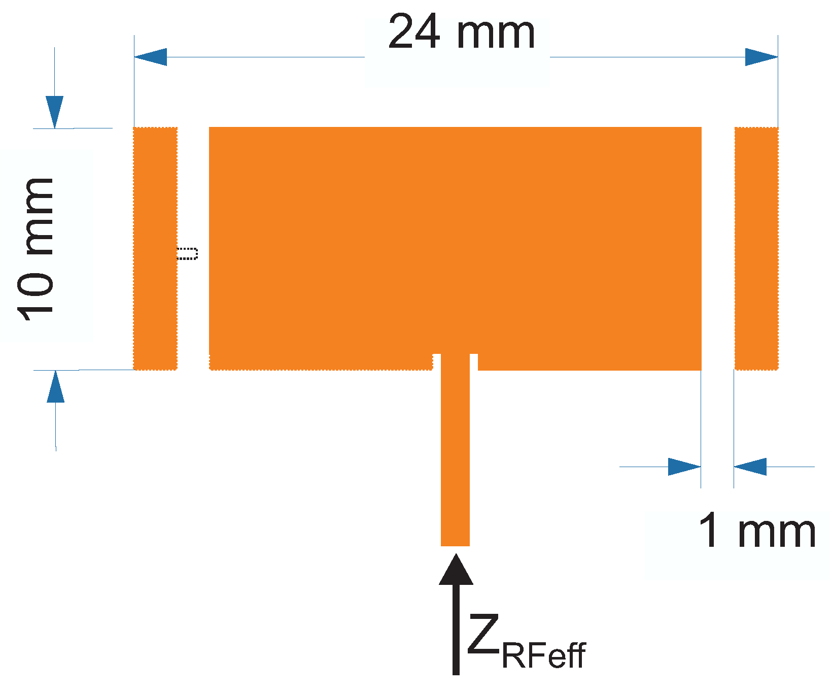
The antenna was designed to satisfy the impedance requirements in terms of and it shows a high level of compactness. The antenna topology is based on a single patch antenna printed on the same substrate of the cold-FET backscattering modulator and the three-stage RF–DC converter, namely the Isola FR408 (, ). The antenna was designed at GHz in order to show an input impedance of = . This non-canonical input impedance value was obtained by using a couple of patches etched on the same plane of the patch itself. Their presence adds an additional degree of freedom in the antenna design, which allows for achieving the desired input impedance. The antenna was simulated with a commercial full-wave electromagnetic simulator. The resulting antenna layout, which is inspired by the one proposed in [25], is shown in Figure 7, where the main dimensional parameters are also illustrated.
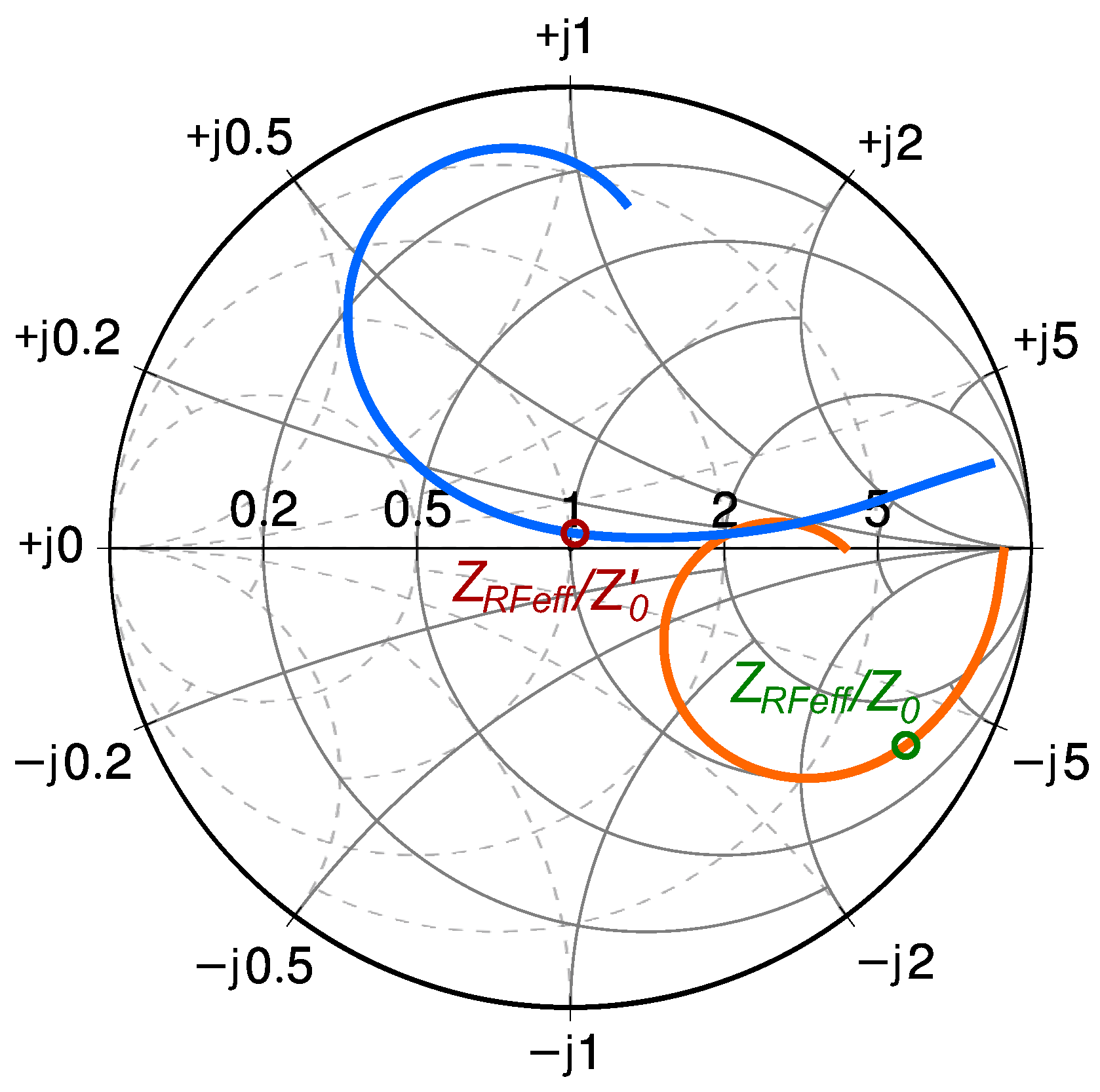
The proposed design shows an antenna gain of about 6 dBi as well as an antenna efficiency of about 71.4%. The simulated antenna reflection coefficient is illustrated in Figure 8 in a band of about 1.6 GHz and is centered on 5.8 GHz. The parameter is evaluated with respect to the usual normalization impedance and the optimum impedance . The circle in the graph represents the different normalization impedance values of @ 5.8 GHz. The Smith chart confirms that the concept of optimum matching for this application is completely different from the usual matching approach.
3. The BackCom Node Prototype
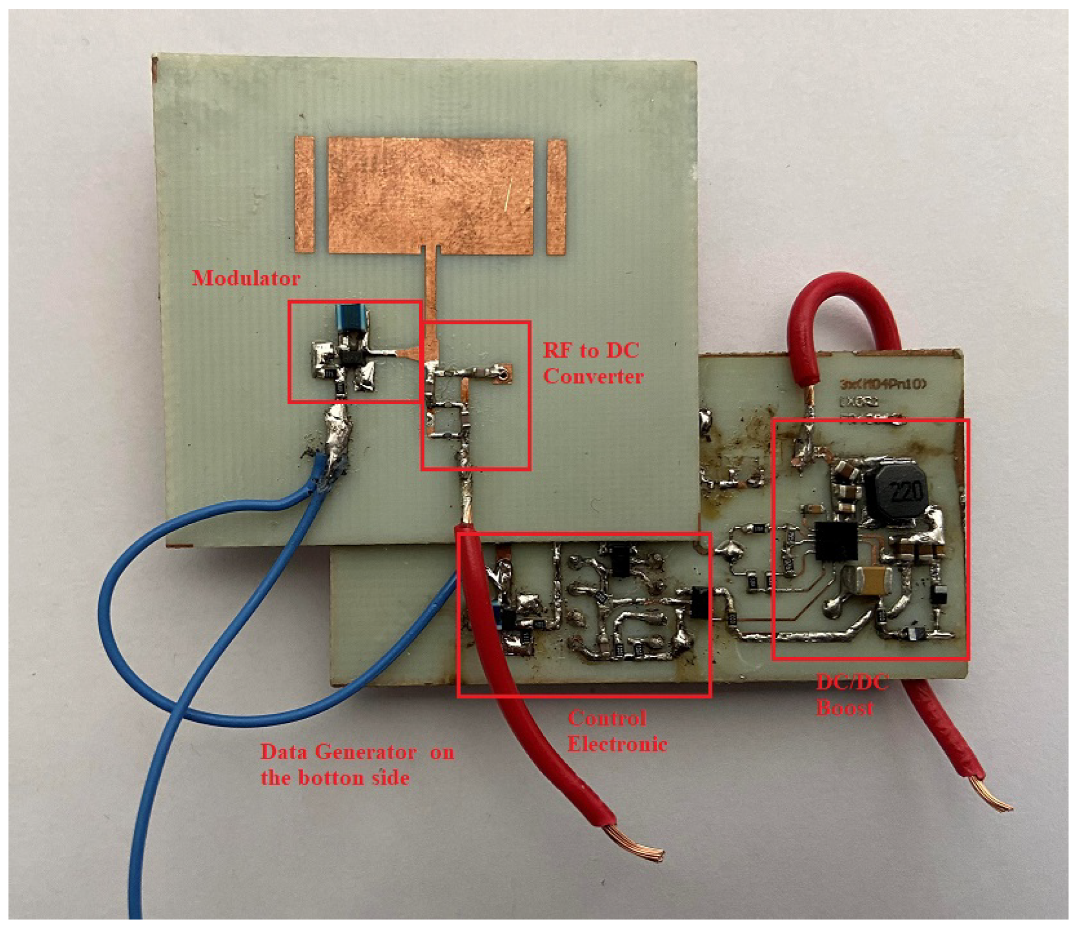
The prototype was implemented by making use of two different boards. The first one integrates the optimum matched antenna, the modulator, and the RF to DC converter, while the second board includes the DC–DC boost device, the control electronics, and the data generator. This approach simplifies the development of prototypes as well as the testing phase, allowing for full control over all critical blocks and enabling the measurement of key parameters. The two boards were implemented on the Isola FR408 laminate and the prototypes are illustrated in Figure 9.
The modulator is based on an ATF58143 pseudomorphic HEMT in a cold-FET configuration; the voltage tripler (RF to DC converter) employs three silicon, zero bias SMS7630-061 Schottky detector diodes; the DC–DC boost is based on the commercial BQ25570 [22]. Furthermore, concerning the critical components of the DC/DC converter illustrated in Figure 1, and are the values of 22 μH and 100 F. The data generator is based on an EEPROM, Atmel AT17LV512A 3.3 V 256 kbit on a PDIP package [26], which emulates the controller block.
4. The BackCom Node Prototype’s Experimental Results
In order to assess the performance of the proposed batteryless BackCom node architecture as a whole, a specific measurement setup was implemented. In particular, it was conceived to investigate the backscattering communication behavior and the performance of the harvester in different conditions.
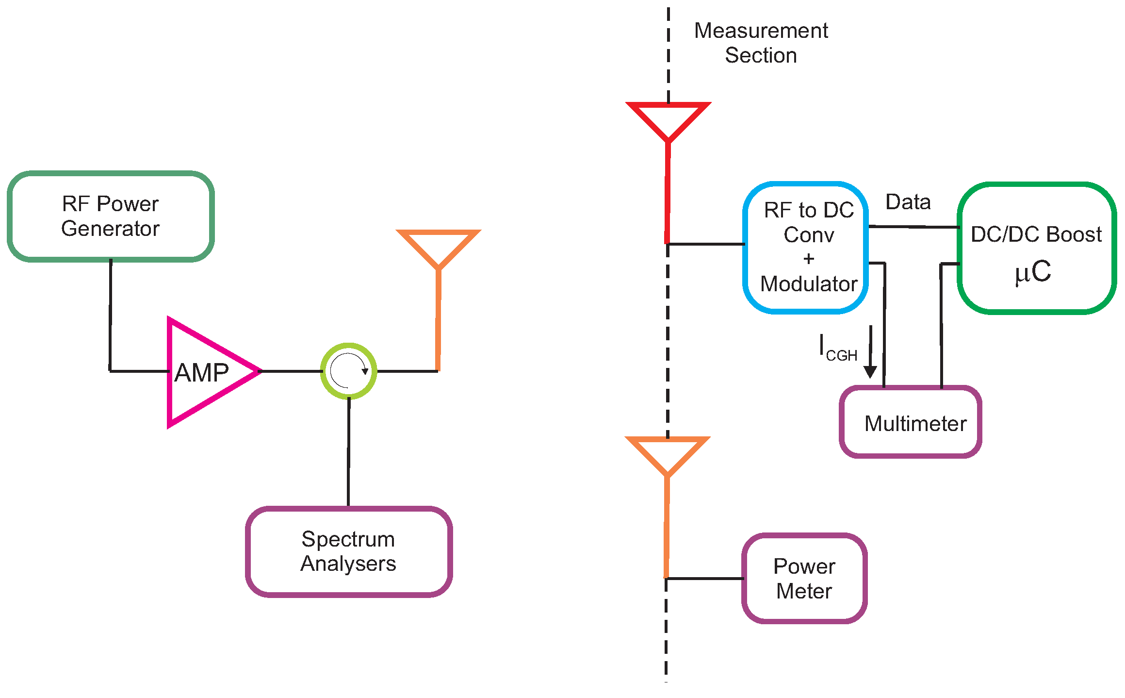
The measurement setup schematic is illustrated in Figure 10, and consists of a radio link with the node under test from one side and a TX/RX system from the other side. The node, being implemented in the split form illustrated in Section 3, simplifies the testing procedure. Such a configuration allows for accessing the terminal between the RF to DC converter and the DC/DC boost, enabling the measurement of the , as well as the data line monitoring. On the contrary, the TX/RX system makes use of an RF power generator and a power amplifier in the transmitter path, while the receiver is implemented by means of a spectrum analyzer. The two paths are connected to a single antenna array through a circulator.
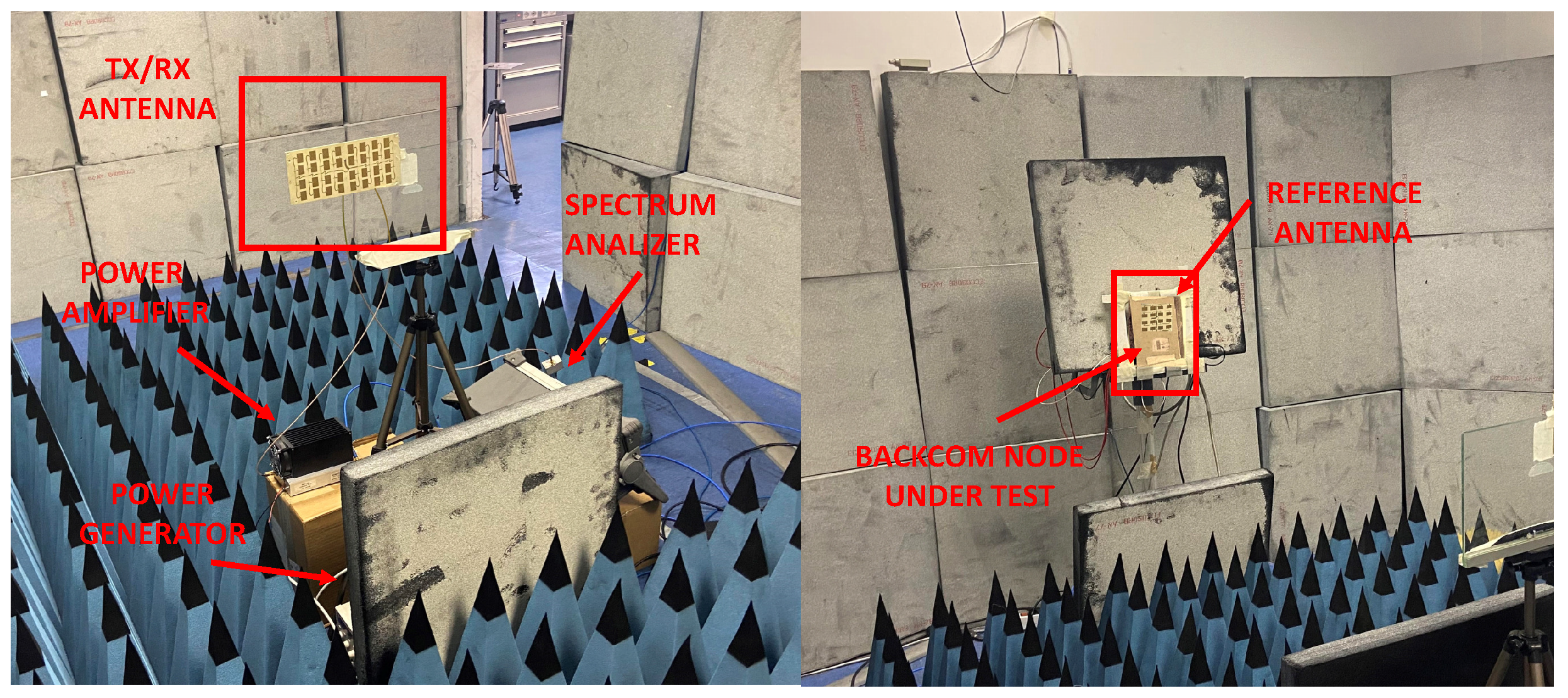
The previously described setup includes a reference antenna on the same BackCom node measurement section. The latter is connected to a power meter in order to evaluate, at the reference section, the effective impinging power. Based on this setup, the BackCom node behavior was characterized. The implemented measurement setup is illustrated in Figure 11
The distance between the reader TX/RX antenna and the node was fixed at 1.8 m in the setup; in addition, the main dimension of such an antenna resulted in 0.25 m, with an EIRP = 37 dB, while the antenna that was integrated in the node showed a gain of about 6 dBi. Therefore, in accordance with the operative data, the limits for the far-field and the near-field are m (far-field limit) and m (near-field limit). Consequently, the system was not tested in either far-field or near-field conditions. The system was characterized in an anechoic setup to take advantage of the absorbing behaviors of the absorbers. Our objective was to obtain reliable data from the characterization by isolating the setup as much as possible from unpredictable environmental contributions, rather than eliminating all of the possible multipath contributions. The data features confirmed the reliability of the measurement setup.
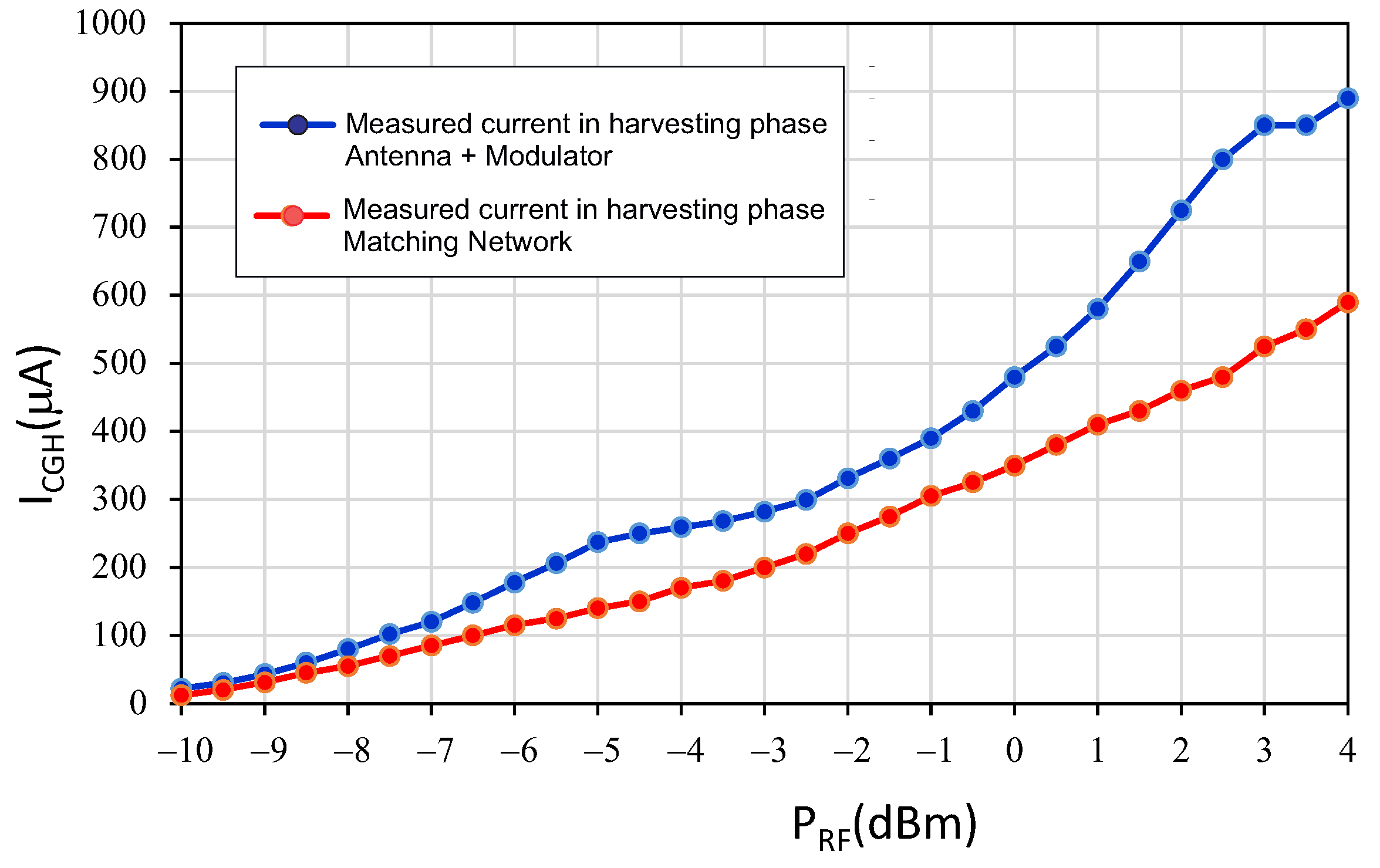
The first set of tests was aimed at verifying the effective improvement of the harvesting performance of the node. The results are illustrated in Figure 12 and Figure 13. The measurements confirm that the node was effectively designed to simultaneously follow the approach of the optimum matched antenna and the minimization of the modulator effect during the harvesting phase (3).
Figure 12 compares the of the proposed architecture with respect to the one exhibited by a standard configuration, using a matching network to implement the optimum impedance. The latter does not include the modulator block. was evaluated in both configurations, considering the same RF power at the RF to DC converter input by means of the power meter connected to the reference antenna, and taking into account the optimum antenna gain. The architecture proposed in the present paper has demonstrated an overall improvement in at every input power level. In particular, at the design reference, the RF power is about −5 dBm (at the input of the RF to DC converter section), and the measured current is 237 A for the node and 145 A for the standard structure with an improvement of about 92 A.
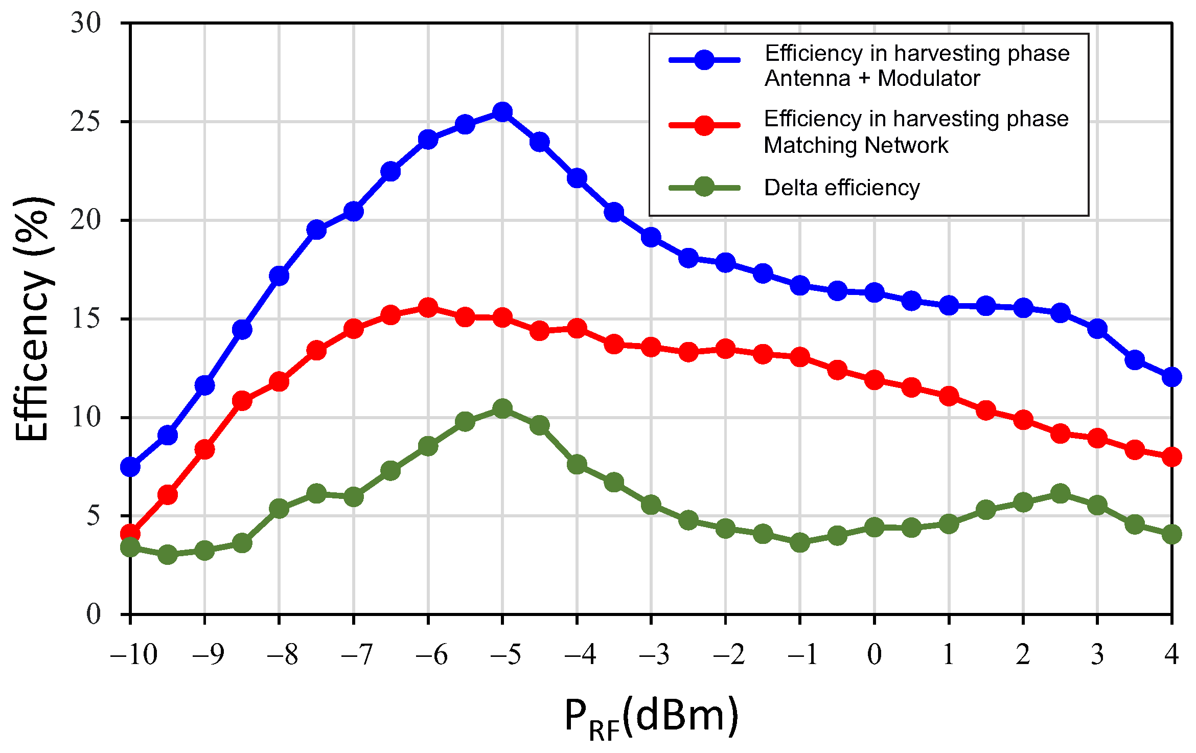
Figure 13 illustrates the efficiency of the same two configurations. The measurements confirm that the harvesting efficiency of the BackCom node is improved compared to the standard configuration across the entire range of input power levels. Here, the efficiency is calculated as the ratio of the power supplied to the DC/DC with respect to the impinging power at the input of the RF to DC converter, as described in
Moreover, the above-mentioned figure also shows the incremental efficiency (), which was calculated as the difference between the two cases at each power level.
With reference to (5), at −5 dBm of the RF input power (the design reference level), the node shows an efficiency of about , while the standard configuration is at about . This leads to an increased harvester efficiency of about , which translates to a reduction of the charging time for a given storage capacitor.
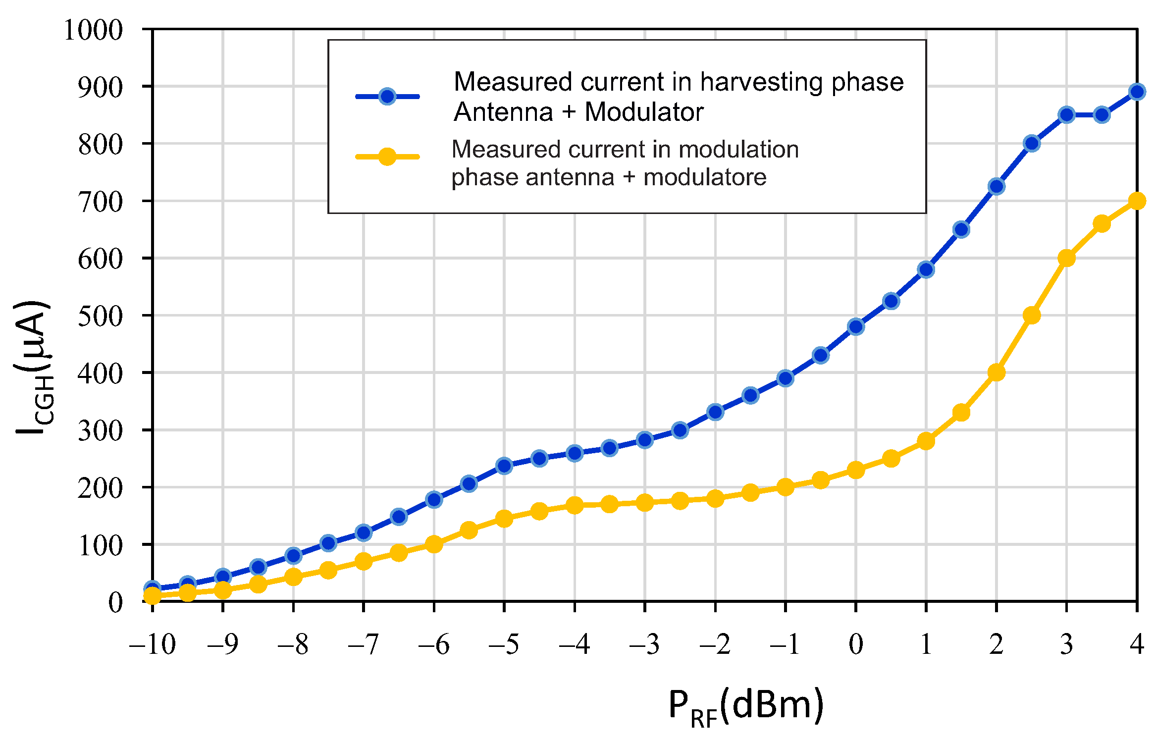
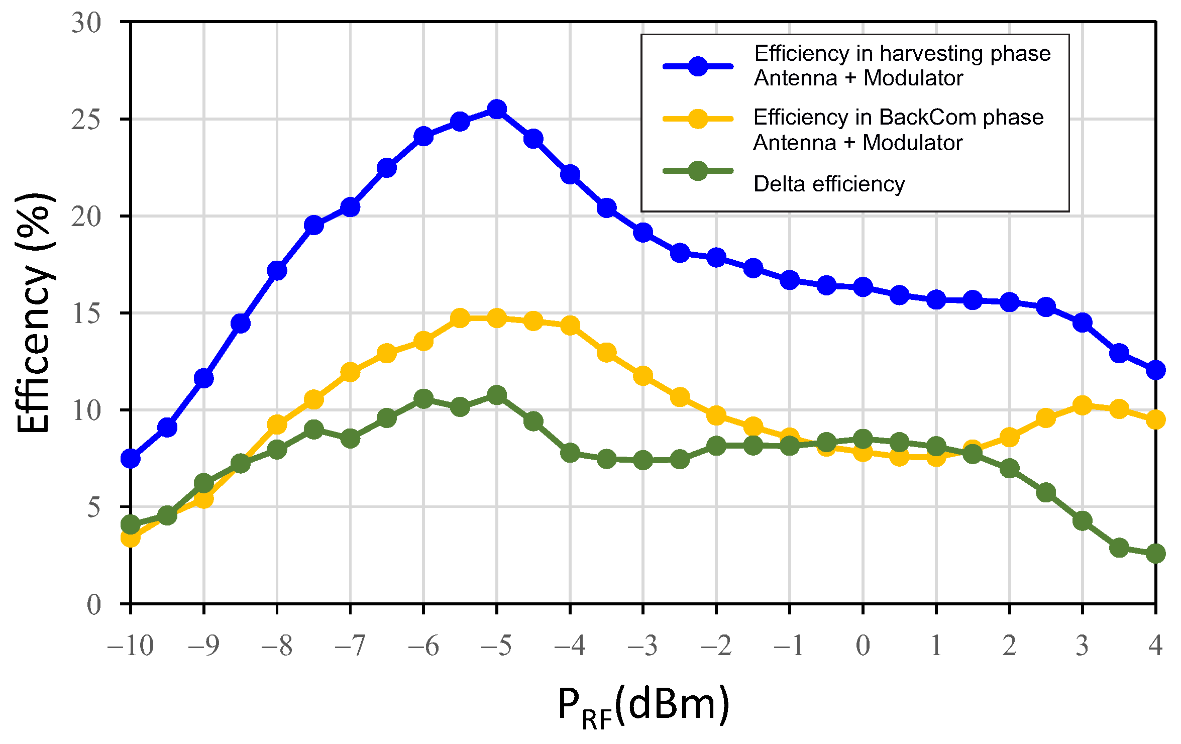
The same measurement setup was used to evaluate the harvesting performance of the node during the backscattering condition. Figure 14 illustrates the behavior of the charge current in querying and backscattering state. This result confirms, as expected, the reduced harvesting performance during the communication period. At the input power RF reference level (−5 dBm), in the backscattering state assumes a value of about 137 A. This value is 99 A lower than the harvesting state, which measures 237 A. These measures show how the node maintains a harvesting performance similar to the one shown by the standard configuration implementing the matching network (during the backscattering communication). The ability of the node to harvest energy during the backscattering state is confirmed by Figure 15, which compares the efficiencies of the two functional states and highlights the delta between them.
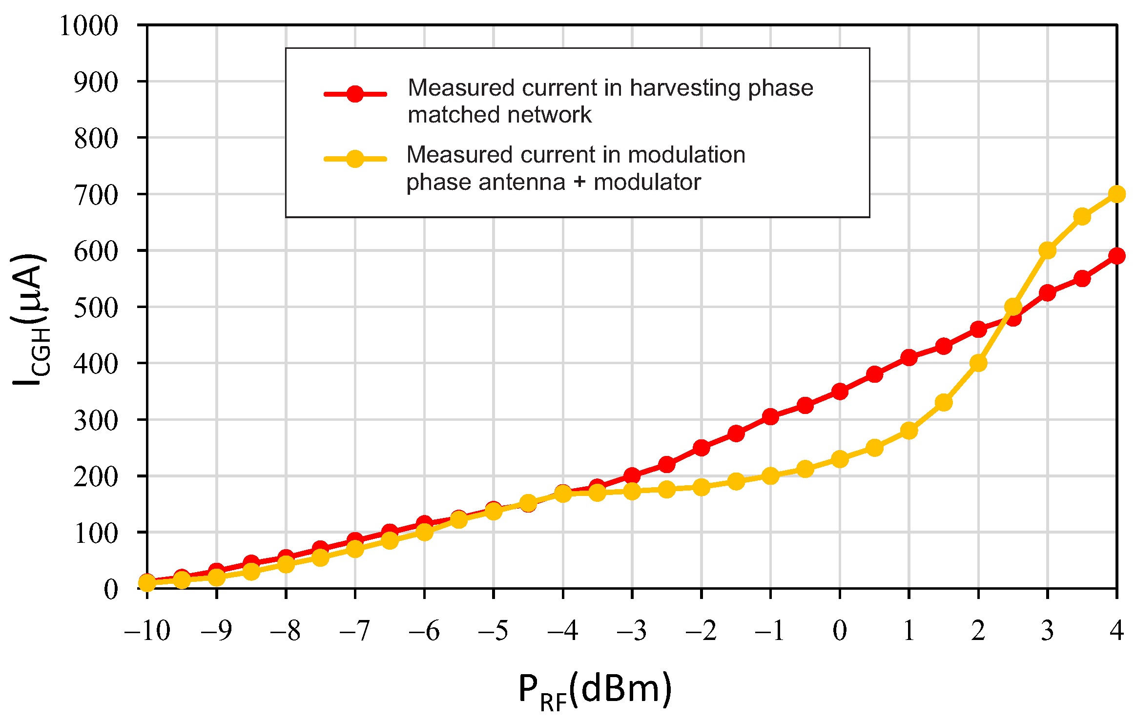
Figure 16 confirms that the comparison between (supplied by the node in the backscattering state) and the corresponding value in the standard configuration (implementing the matching network in the harvesting state) are very similar across all input power levels. This behavior contributes significantly to delaying the discharge of and, as a consequence, increases the time slot for communication.
A state-of-the-art analysis was carried out in order to compare the harvesting performance shown by the proposed architecture in comparison with other approaches; the results are summarized in Table 1. The harvester performances of the architecture proposed in the present work were evaluated with respect to two solutions proposed by the same authors, operating at 5.8 GHz, as well as four solutions proposed by different authors, three of which work at 5.8 GHz and one at 2.45 GHz. In References [21,27], the performances are evaluated under operating conditions when the system is connected to the BQ25570. The first makes use of a matching network that introduces losses and shows (at −5 dBm) an efficiency of about , while the second adopts a matching network optimized for multi-sine excitation; it shows performance improvements of up to at −5 dBm. The latter shows better performances with respect to the present work but it is not fully compatible with the BackCom approach; it is more oriented to pure harvesting solutions. With respect to the solutions described in [28,29,30], they operate at 5.8 GHz, while the solution described in [31] operates at 2.45 GHz.
The first shows an efficiency of about at −5 dBm, the second demonstrates an efficiency of about at −10 dBm, and the third exhibits an efficiency of about at −5 dBm. The fourth, which works at 2.45 GHz, shows an efficiency of about at −10 dBm. Some of these solutions show better efficiencies compared to the present work. The main drawback consists is that they were not evaluated in operational conditions but rather with optimal loads of high value (k order of magnitude). As a consequence, considering the system-level operative conditions, the approach proposed in the present work performed better compared to all other state-of-the-art architectures.
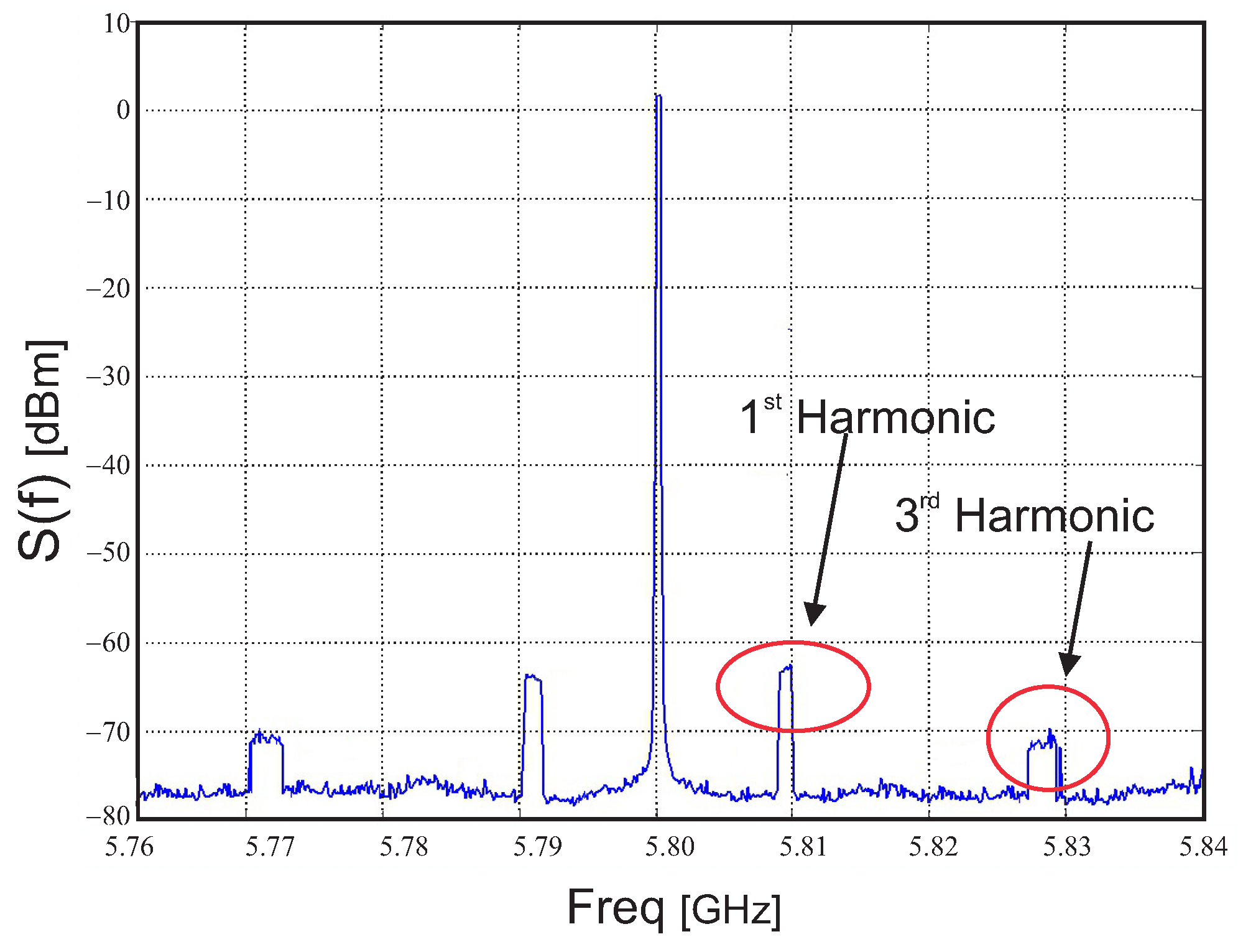
The system ability of the proposed architecture to implement an ASK backscattering communication was evaluated by driving the proposed cold-FET modulator by means of a 10 MHz square wave (i.e., a periodic sequence of bit 0 and bit 1), which was generated by the EEPROM, which emulates the controller block. Such a modulating signal provides a reference benchmark for testing the harvesting efficiency in the backscattering phase due to its inherently fixed frequency rate. The setup that was implemented to detect the spectrum of the backscattered signal modulated by the square wave refers to the block diagram, as illustrated in Figure 10.
The results are illustrated in Figure 17, showing the spectrum of the backscattered signal modulated by the square wave. The figure illustrates the signal spectrum across the carrier, where the fundamental, as well as the third harmonic of the modulating signal, are recognizable. The EEPROM, emulating the controller block, is active for the discharging time interval (i.e., , as stated in [21]) for a maximum of 360 ms, which is independent from the impinging power. On the contrary, the charge time interval depends directly on the latter. For a power level of about −5 dBm at the input of the RF to DC converter, measurements show a charging time of 27 s. However, the discharge is a slightly critical phase for the modulation. As a matter of fact, the decrease in affects the performance of the EEPROM, which in the final part of generates a square wave with a frequency that is below the canonical 10 MHz. As a consequence, both the spectrum of the first and third harmonics show a slight widening.
Based on the previously described backscattering experiment with a modulating square wave signal of 10 MHz, it is possible to argue that this value can be assumed as the maximum data rate. The conversion gain of the node in the backscattering mode was estimated to be 2.7 dB; this enables a typical operative range of 1 m, depending on the reader’s EIRP and sensitivity. Regarding power consumption, it is not considered a relevant figure in this context since the component is batteryless.
Consequently, the measured results and analysis conducted in the proposed critical functional block assessment in this paper demonstrate the feasibility of a batteryless BackCom node, as postulated in [32].
5. Conclusions
In this paper, we demonstrated the feature of the key functional blocks for a BackCom node, enabling an integrated architecture for a totally batteryless BackCom node. In particular, the coexistence of a highly efficient harvester configuration, a cold-FET-based modulator, and an antenna designed to exhibit the optimum impedance for maximum charging performances was fully demonstrated. The inclusion of such an antenna leads to an improvement of 63% in the harvesting current, increasing the value from 145 A to 237 A, with respect to the identical configuration involving a microstrip-matching network coupled with a typical 50- patch antenna. The conversion efficiency in operative conditions demonstrates an improvement from 15% to 25.5%. Moreover, the effectiveness of the ASK modulation was demonstrated. In summary, the performance comparison of the system proposed in this paper, with respect to comparable technologies, shows that this node system exhibits the best efficiency in operative conditions.
Author Contributions
Conceptualization, A.C. and G.C.; methodology, G.C. and M.P.; data curation, M.R.; validation, G.C.; formal analysis, M.P. and A.C.; investigation, A.C.; resources, G.C. and A.C.; writing—original draft preparation, G.C.; writing—review and editing, A.C.; visualization, G.C. and M.R.; supervision, A.C.; project administration, A.C.; funding acquisition, G.C. All authors have read and agreed to the published version of the manuscript.
Funding
This research received no external funding.
Institutional Review Board Statement
Not applicable.
Informed Consent Statement
Not applicable.
Data Availability Statement
Not applicable.
Conflicts of Interest
The authors declare no conflict of interest.
References
- Mishu, M.K.; Rokonuzzaman, M.; Pasupuleti, J.; Shakeri, M.; Rahman, K.S.; Hamid, F.A.; Tiong, S.K.; Amin, N. Prospective Efficient Ambient Energy Harvesting Sources for IoT-Equipped Sensor Applications. Electronics 2020, 9, 1345. [Google Scholar] [CrossRef]
- Tubis, A.A.; Rohman, J. Intelligent Warehouse in Industry 4.0—Systematic Literature Review. Sensors 2023, 23, 4105. [Google Scholar] [CrossRef]
- De Capua, C.; Fulco, G.; Lugarà, M.; Ruffa, F. An Improvement Strategy for Indoor Air Quality Monitoring Systems. Sensors 2023, 23, 3999. [Google Scholar] [CrossRef]
- Chen, W.; Zhang, Z.; Hong, Z.; Chen, C.; Wu, J.; Maharjan, S.; Zheng, Z.; Zhang, Y. Cooperative and distributed computation offloading for blockchain-empowered industrial Internet of Things. IEEE Internet Things J. 2019, 6, 8433–8446. [Google Scholar] [CrossRef]
- Bartoli, C.; Bonanni, M.; Chiti, F.; Pierucci, L.; Cidronali, A.; Collodi, G.; Maddio, S. Toward the Web of Industrial Things: A Publish-Subscribe Oriented Architecture for Data and Power Management. Sensors 2022, 22, 4882. [Google Scholar] [CrossRef]
- Liu, W.; Huang, K.; Zhou, X.; Durrani, S. Next generation backscatter communication: Systems, techniques, and applications. EURASIP J. Wirel. Commun. Netw. 2019, 2019, 69. [Google Scholar] [CrossRef]
- Khriji, S.; Chéour, R.; Kanoun, O. Dynamic Voltage and Frequency Scaling and Duty-Cycling for Ultra Low-Power Wireless Sensor Nodes. Electronics 2022, 11, 4071. [Google Scholar] [CrossRef]
- Cidronali, A.; Nair, V.; Collodi, G.; Lewis, J.H.; Camprini, M.; Manes, G.; Goronkin, H. MMIC applications of heterostructure interband tunnel devices. IEEE Trans. Microw. Theory Tech. 2003, 51, 1351–1367. [Google Scholar] [CrossRef]
- Torres, R.; Pereira, F.; Correia, R.; Carvalho, N.B. An All-Digital Ambient Backscatter solution powered by Energy Harvesting. In Proceedings of the 2021 IEEE MTT-S International Microwave and RF Conference (IMARC), Kanpur, India, 17–19 December 2021; pp. 1–3. [Google Scholar]
- Rezaei, F.; Galappaththige, D.; Tellambura, C.; Herath, S. Coding Techniques for Backscatter Communications—A Contemporary Survey. IEEE Commun. Surveys Tutor. 2023. [Google Scholar] [CrossRef]
- Niu, J.P.; Li, G.Y. An Overview on Backscatter Communications. J. Commun. Inf. Netw. 2019, 4, 1–14. [Google Scholar] [CrossRef]
- Wu, W.; Wang, X.; Hawbani, A.; Yuan, L.; Gong, W. A survey on ambient backscatter communications: Principles, systems, applications, and challenges. Comput. Netw. 2022, 216, 109235. [Google Scholar] [CrossRef]
- Memon, M.L.; Saxena, N.; Roy, A.; Shin, D.R. Backscatter Communications: Inception of the Battery-Free Era—A Comprehensive Survey. Electronics 2019, 8, 129. [Google Scholar] [CrossRef]
- Khan, W.U.; Memon, F.H.; Dev, K.; Javed, M.A.; Do, D.T.; Qureshi, N.M.F. Ambient BackCom in beyond 5G NOMA networks: A multi-cell resource allocation framework. Digit. Commun. Netw. 2022, 8, 1005–1013. [Google Scholar] [CrossRef]
- Correia, R.; Carvalho, N.B.; Kawasaki, S. Continuously Power Delivering for Passive Backscatter Wireless Sensor Networks. IEEE Trans. Microw. Theory Tech. 2016, 64, 3723–3731. [Google Scholar] [CrossRef]
- Belo, D.; Correia, R.; Pinho, P.; Carvalho, N.B. Enabling a constant and efficient flow of wireless energy for IoT sensors. In Proceedings of the IEEE MTT-S International Microwave Symposium (IMS), Honololu, HI, USA, 4–9 June 2017; pp. 1342–1344. [Google Scholar]
- Qaragoez, Y.; Pollin, S.; Schreurs, D. FDD for Low Power Backscattering in Batteryless Sensor Nodes. In Proceedings of the 51st European Microwave Conference (EuMC), London, UK, 4–6 April 2022; pp. 753–756. [Google Scholar]
- Cidronali, A.; Maddio, S.; Collodi, G.; Manes, G. Design trade-off for a compact 5.8 GHz DSRC transponder front-end. Microw. Opt. Technol. Lett. 2015, 57, 1187–1191. [Google Scholar] [CrossRef]
- Toro, U.S.; Wu, K.; Leung, V.C.M. Backscatter Wireless Communications and Sensing in Green Internet of Things. IEEE Trans. Green Commun. Netw. 2022, 6, 37–55. [Google Scholar] [CrossRef]
- Passafiume, M.; Collodi, G.; Cidronali, A. Optimum Design of Low Energy Harvesting Detector at 5.8 GHz suitable for COTS devices. In Proceedings of the 2019 IEEE International Conference on RFID Technology and Applications (RFID-TA), Pisa, Italy, 25–27 September 2019; pp. 6–10. [Google Scholar]
- Passafiume, M.; Collodi, G.; Cidronali, A. Design Principles of Batteryless Transponder for Vehicular DSRC at 5.8 GHz. IEEE J. Radio Freq. Identif. 2020, 4, 491–505. [Google Scholar] [CrossRef]
- Texas Instruments Incorporated. BQ25570: Nano Power Boost Charger and Buck Converter for Energy Harvester Powered Applications; Texas Instruments Incorporated: Dallas, TX, USA, 2019. [Google Scholar]
- Collodi, G.; Maddio, S.; Pelosi, G. Design of a compact and highly efficient energy harvester system suitable for battery-less low cost on-board unit applications. Electronics 2021, 10, 3. [Google Scholar] [CrossRef]
- Torres, R.; Correia, R.; Carvalho, N.B.; Daskalakis, S.; Goussetis, G.; Ding, Y.; Georgiadis, A.; Eid, A.; Hester, J.; Tentzeris, M.M. Backscatter communications. IEEE J. Microwaves 2021, 1, 864–878. [Google Scholar] [CrossRef]
- Maddio, S.; Pelosi, G.; Righini, M.; Selleri, S. A slotted patch antenna with enhanced gain pattern for automotive applications. Prog. Electromagn. Res. Lett. 2021, 95, 135–141. [Google Scholar] [CrossRef]
- Atmel Corporation. AT17LV512A: FPGA Configuration EEPROM Memory 3.3V and 5.0V; Atmel Corporation: San Jose, CA, USA, 2014. [Google Scholar]
- Passafiume, M.; Collodi, G.; Cidronali, A. Improving Wireless Power Transfer Efficiency With DC/DC Boost Charger by Multi-Sine Excitation at 5.8 GHz. IEEE Microw. Wirel. Components Lett. 2022, 32, 760–763. [Google Scholar] [CrossRef]
- Qi, C.; Frederick, Q.; Davis, K.; Lindsay, D.; Cox, J.; Parke, S.; Griffin, J.D.; Durgin, G.D. A 5.8 GHz Energy Harvesting Tag for Sensing Applications in Space. In Proceedings of the 2018 6th IEEE International Conference on Wireless for Space and Extreme Environments (WiSEE), Huntsville, AL, USA, 11–13 December 2018; pp. 218–223. [Google Scholar]
- Olule, L.J.A.; Gnanagurunathan, G.; Kumar, N.T.; Kasi, B. Single band RF Energy Harvesting at 5.8 GHz using EBG unit cells. In Proceedings of the 2018 IEEE International RF and Microwave Conference (RFM), Penang, Malaysia, 17–19 December 2018; pp. 352–355. [Google Scholar]
- Janhunen, J.; Mikhaylov, K.; Petäjäjärvi, J.; Sonkki, M. Wireless Energy Transfer Powered Wireless Sensor Node for Green IoT: Design, Implementation and Evaluation. Sensors 2019, 19, 90. [Google Scholar] [CrossRef]
- Nguyen, X.V.L.; Gerges, T.; Bevilacqua, P.; Duchamp, J.-M.; Benech, P.; Verdier, J.; Lombard, P.; Linge, P.U.; Mieyeville, F.; Cabrera, M.; et al. Radio-Frequency Energy Harvesting Using Rapid 3D Plastronics Protoyping Approach: A Case Study. J. Low Power Electron. Appl. 2023, 13, 19. [Google Scholar] [CrossRef]
- Han, K.; Huang, K. Wirelessly powered backscatter communication networks: Modeling, coverage, and capacity. IEEE Trans. Wirel. Commun. 2017, 16, 2548–2561. [Google Scholar] [CrossRef]
Figure 1.
Architecture of the considered IoT BackCom batteryless node. The capacitor and the inductance assume values of 100 F and 22 nH, respectively.
Figure 1.
Architecture of the considered IoT BackCom batteryless node. The capacitor and the inductance assume values of 100 F and 22 nH, respectively.

Figure 2.
Conceptualization of the source impedance optimization by the source pull-based technique.
Figure 2.
Conceptualization of the source impedance optimization by the source pull-based technique.

Figure 3.
The modeling of a high impedance state modulator for evaluating .

Figure 4.
Modulator block for the backscattering mode of the BackCom node.

Figure 5.
Modulator impedance with respect to the feeding line dimensions.

Figure 6.
Representation of the and symbols on the Smith chart.

Figure 7.
The main dimensions of the antenna for achieving the optimum impedance.

Figure 8.
The parameter normalized, respectively, to (orange) and (blue).

Figure 9.
BackCom node composed of two boards.

Figure 10.
Measurement setup block diagram.

Figure 11.
Measurement setup for the characterization of the BackCom node.

Figure 12.
Measured current in harvesting the interval for the actual configuration (without a matching network) and with a matching network.
Figure 12.
Measured current in harvesting the interval for the actual configuration (without a matching network) and with a matching network.

Figure 13.
Efficiency in harvesting the interval for the actual configuration (without a matching network) and with a matching network.
Figure 13.
Efficiency in harvesting the interval for the actual configuration (without a matching network) and with a matching network.

Figure 14.
Measured currents in the harvesting state and backscattering state, with a modulating square wave at 10 MHz.
Figure 14.
Measured currents in the harvesting state and backscattering state, with a modulating square wave at 10 MHz.

Figure 15.
Efficiencies in the harvesting state and backscattering state.

Figure 16.
Measured current in the harvesting state with the matched network and in the harvesting state.
Figure 16.
Measured current in the harvesting state with the matched network and in the harvesting state.

Figure 17.
Measured spectrum of the backscattered signal modulated by a 10 MHz square wave.


Table 1.
Harvesting performance comparison of the system working @ 5.8 GHz.
| Reference | Reference Power (dBm) | Eff. (%) | Freq. (GHz) | Load/Condition |
|---|---|---|---|---|
| [21] | −5 | 16 | 5.8 | BQ25570 operative condition |
| [28] | −5 | 22 | 5.8 | 3 k |
| [31] | −10 | 35 | 2.45 | 5 k |
| [27] | −5 | 27 | 5.8 | BQ25570 operative condition |
| [29] | −10 | 15 | 5.8 | 10 k |
| [30] | −5 | 51 | 5.8 | 9 k |
| This work | −5 | 25.5 | 5.8 | BQ25570 operative condition |
Disclaimer/Publisher’s Note: The statements, opinions and data contained in all publications are solely those of the individual author(s) and contributor(s) and not of MDPI and/or the editor(s). MDPI and/or the editor(s) disclaim responsibility for any injury to people or property resulting from any ideas, methods, instructions or products referred to in the content. |
© 2023 by the authors. Licensee MDPI, Basel, Switzerland. This article is an open access article distributed under the terms and conditions of the Creative Commons Attribution (CC BY) license (https://creativecommons.org/licenses/by/4.0/).
Share and Cite
MDPI and ACS Style
Collodi, G.; Righini, M.; Passafiume, M.; Cidronali, A. Energy Efficient Enhancement in a 5.8 GHz Batteryless Node Suitable for Backscattering Communications. Electronics 2023, 12, 2256. https://doi.org/10.3390/electronics12102256
AMA Style
Collodi G, Righini M, Passafiume M, Cidronali A. Energy Efficient Enhancement in a 5.8 GHz Batteryless Node Suitable for Backscattering Communications. Electronics. 2023; 12(10):2256. https://doi.org/10.3390/electronics12102256
Chicago/Turabian StyleCollodi, Giovanni, Monica Righini, Marco Passafiume, and Alessandro Cidronali. 2023. "Energy Efficient Enhancement in a 5.8 GHz Batteryless Node Suitable for Backscattering Communications" Electronics 12, no. 10: 2256. https://doi.org/10.3390/electronics12102256
Note that from the first issue of 2016, this journal uses article numbers instead of page numbers. See further details here.