Article

Selective Area Epitaxy of GaAs/Ge/Si Nanomembranes: A Morphological Study

1
Institute of Photonics and Nanotechnologies—CNR, P.za L. Da Vinci, 20133 Milano, Italy
2
Department of Materials Science, University of Milano – Bicocca, via R. Cozzi 55, 20125 Milano, Italy
3
Department of Physics, Politecnico di Milano, P.zza L. da Vinci, 20133 Milano, Italy
*
Author to whom correspondence should be addressed.
Crystals 2020, 10(2), 57; https://doi.org/10.3390/cryst10020057
Submission received: 19 December 2019 / Revised: 20 January 2020 / Accepted: 21 January 2020 / Published: 22 January 2020
(This article belongs to the Special Issue Semiconductor Heteroepitaxy)

Abstract

:
We demonstrate the feasibility of growing GaAs nanomembranes on a plastically-relaxed Ge layer deposited on Si (111) by exploiting selective area epitaxy in MBE. Our results are compared to the case of the GaAs homoepitaxy to highlight the criticalities arising by switching to heteroepitaxy. We found that the nanomembranes evolution strongly depends on the chosen growth parameters as well as mask pattern. The selectivity of III-V material with respect to the SiO2 mask can be obtained when the lifetime of Ga adatoms on SiO2 is reduced, so that the diffusion length of adsorbed Ga is high enough to drive the Ga adatoms towards the etched slits. The best condition for a heteroepitaxial selective area epitaxy is obtained using a growth rate equal to 0.3 ML/s of GaAs, with a As BEP pressure of about 2.5 × 10⁻⁶ torr and a temperature of 600 °C.

1. Introduction

In the quest for advanced opto-electronic materials, the integration of III–V semiconductor devices with silicon technology is one of the most topical challenges. The exploitation of the optical and electronic know-how of III–V technology, along with the signal processing capabilities and advanced low-cost volume production techniques associated with silicon, is an important goal for the new opto-electronic devices [1]. The approach to the realization of semiconductor devices is different depending on the choice of the substrate, Si versus III-V. Moreover, the material technologies needed and the industrial processing procedures are also significantly different. Therefore, the III-V based devices have met a major barrier to integration so far. However, advances over the last decade in areas such as die transfer, wafer fusion and epitaxial growth have promoted widespread renewed interest [2,3].
Heteroepitaxial growth could be an effective method for III-V/Si integrated device fabrication, although several issues remain unsolved [4,5,6]. First, the zincblende lower symmetry of GaAs compared to the diamond one of Si (or Ge) returns the formation of antiphase domains (APD). Second, the differences in lattice parameters and thermal expansion coefficients between Si and GaAs (approx. 4.2% and 123% respectively) generate defects (such as dislocations) during growth, which are detrimental to the material performance [7]. While relaxing the misfit strain, dislocations often negatively affect the optical and electrical properties of active layers. In particular, threading dislocations (TDs) reaching the surface may drastically decrease lifetime and mobility of the carriers. Wafer bowing and crack formation may even occur when considering thermal processing, especially in the case of micrometer-thick films [8].
A possible solution to overcome the issues related to lattice mismatch consists of using Ge as a substrate for the following heteroepitaxial growth. Ge, indeed, has the same lattice parameter of GaAs and can then be used as a misfit-free substrate. Moreover, Ge can be conveniently deposited on a Si wafer to form a plastically relaxed intermediate layer on top of which GaAs can be grown without strain, thus behaving as a virtual substrate for the fabrication of CMOS-compatible GaAs/Ge/Si heterostructures [9,10].
Selective area epitaxy (SAE) approach can be exploited to grow three-dimensional (3D) GaAs nano-structures, not achievable by direct deposition onto a bare substrate [11,12]. The idea consists of passivating the Ge surface by an oxide layer and confining the epitaxial semiconductor growth into openings defined in the mask by a top-down lithographic approach. A careful optimization of the growth parameters [13], i.e., temperature, deposition flux, and III/V ratio, is required to exclude spurious growth on the masked regions in order to achieve perfect selectivity. Several examples of homoepitaxial growth by SAE have been reported in the literature for III-V nanostructures, such as quantum dots, nanowires, and nanomembranes [6,11,14,15,16,17].
In the present study, we focus on the achievement of 3D GaAs nanomembranes of regular morphology integrated on a Si wafer. To such a goal, a Ge virtual substrate is exploited by depositing Ge on the Si (111) wafer, to accommodate the GaAs lattice parameter to the bare substrate. The use of SAE within small area regions also offers the advantage of reducing the statistical probability to intersect defects (e.g., threading dislocations) originated by the mismatched Ge/Si interface. The study is conducted in close parallelism with the previously reported analysis for the homoepitaxial case of 3D GaAs nanomembranes on GaAs (111)B substrate, in particular with the work by Albani et al. in Ref. [18] where a detailed study of the fin morphology as a function of the slit orientation was discussed. Results here obtained are benchmarked to the ones obtained by homoepitaxy on the same patterns in Ref. [18] to assess the impact of using the Ge virtual substrate on the selective growth of GaAs. Here, we describe how a suitable tuning of the growth conditions permits achieving well-faceted morphologies consistent with the homoepitaxial one, thus offering a first proof-of-concept of the integration of GaAs nanomembranes on Ge/Si substrates by selective area growth.

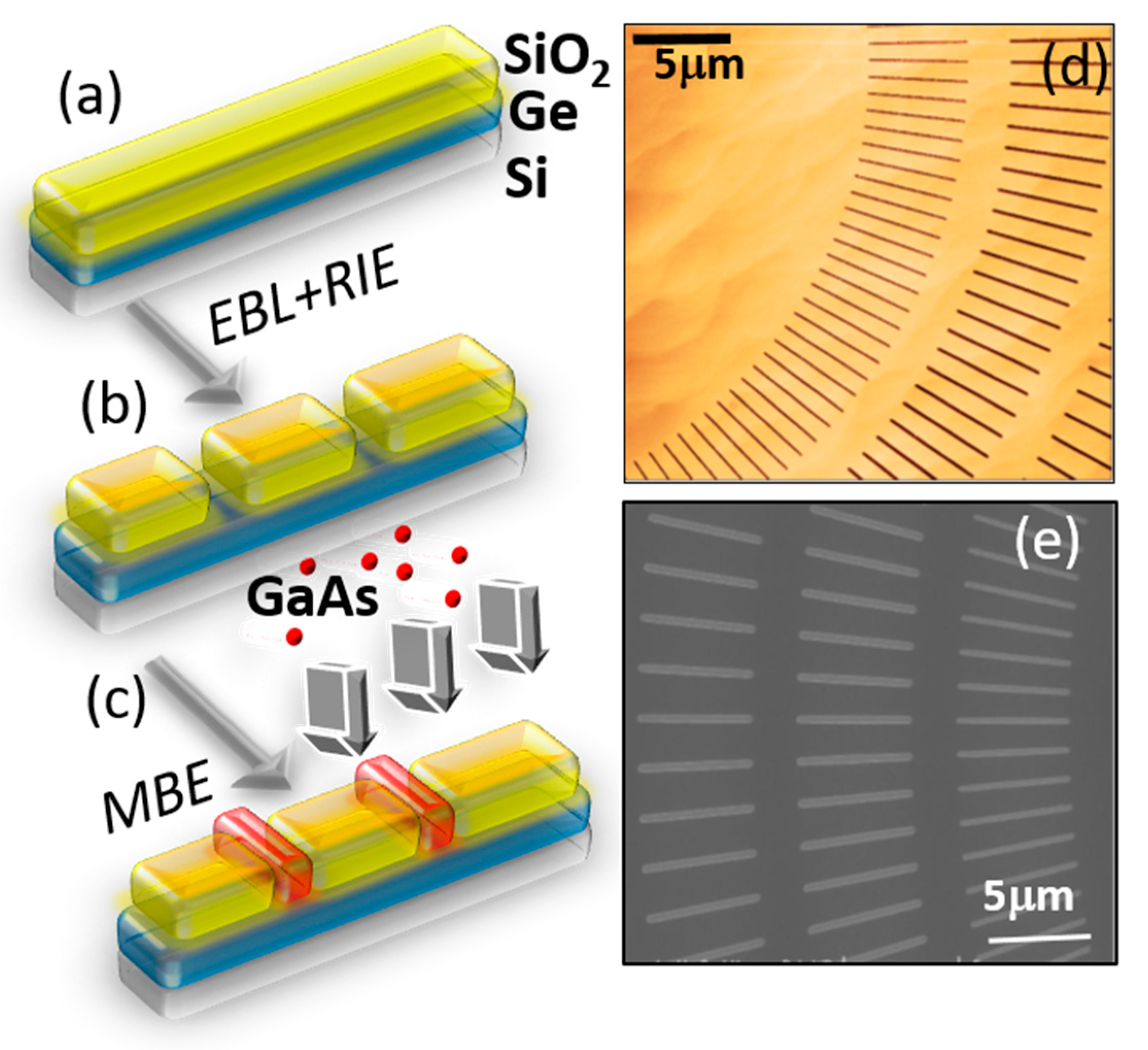
2. Materials and Methods
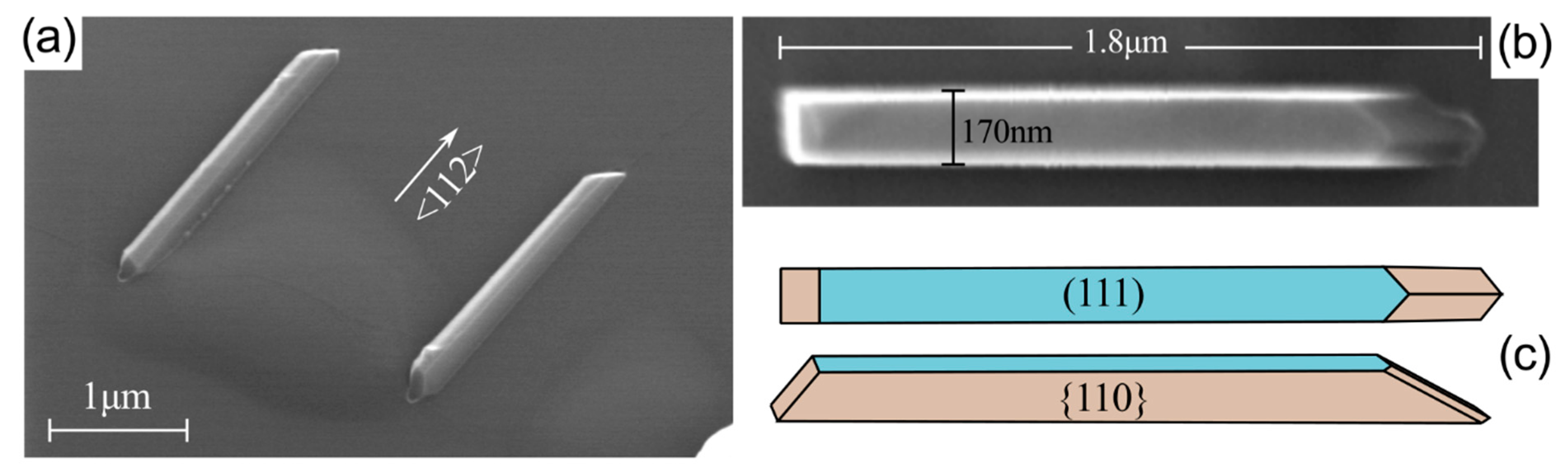
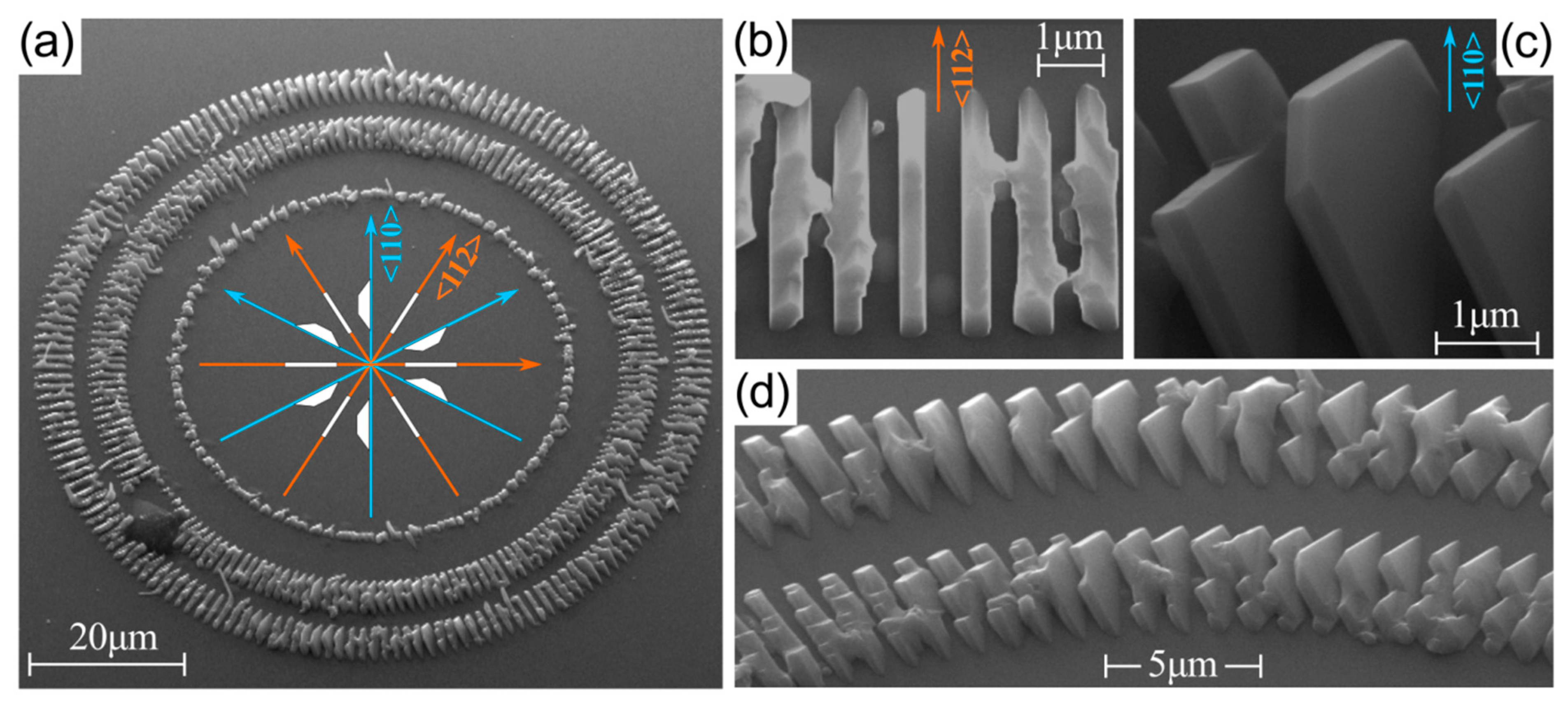
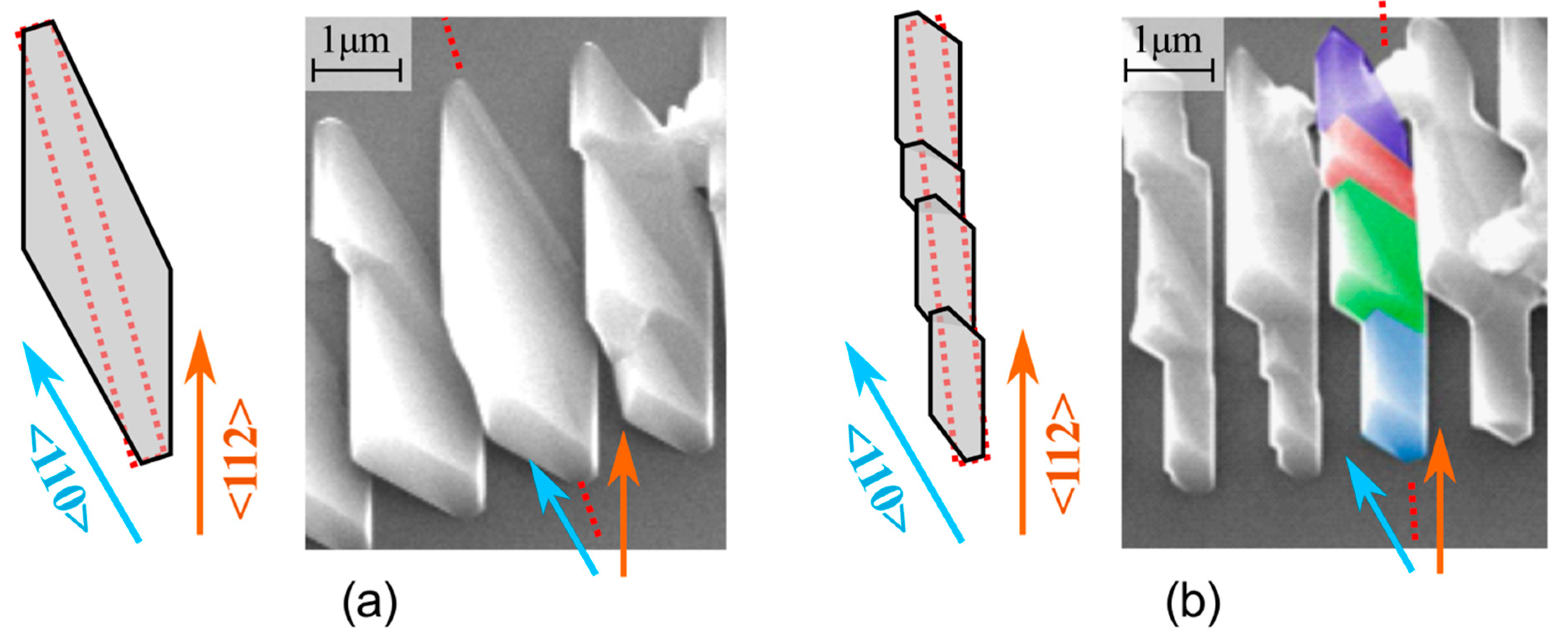
Ge deposition and threading dislocations characterization: a 1 µm thick slightly n-doped Ge (n = 4 × 1015 cm−3) film is grown on 4° miscut Si (111) substrates by low-energy plasma-enhanced chemical vapor deposition (LEPECVD), using a deposition rate of about 4 nm/s at 500 °C [19]. An in-situ annealing procedure over six cycles, between 600 and 800 °C, is performed in order to reduce the threading dislocations density below 7.0 ± 0.5 × 107 cm−2. Specifically, during each cycle, the temperature is increased from 600 to 750 °C in ≈3 min, the samples are then held between 750–800 °C for ≈2 min before being cooled down to 600 °C in ≈1 min. This is a typical procedure to reduce the threading dislocation density from 109 to 107 cm−2 [20]. Preferential etching techniques are used to estimate the threading dislocation density in the Ge thick film, using a solution of 10 mL HF (50% vol) + 15 mL HNO3 (69% vol) + 1 mg KI + 1 mg I2 + 5 mL CH3COOH (100%vol) + 60 mL H2O at 0 °C temperature for 30 s [21,22]. Counting statistics is performed on Ge etched surfaces imaged by atomic force microscopy (AFM).
Sample preparation: a Ge layer is deposited on a miscut Si (111) as previously described. Then, a layer of 30 nm SiO2 is deposited on the Ge surface by atomic layer deposition (ALD) (Figure 1a). Hence, the positive PMMA resist is spin-coated on the SiO2 layer, which in turn is exposed to the electron beam lithography (EBL) process to define the desired patterns. During the lithographic step, different doses are used to create slits with widths of 80–300 nm, lengths between 1–5 µm and slit center spacings of 1–5 µm. The aperture in the oxide film is obtained by the reactive ion etching (RIE) process using CF4 as etchant gas (Figure 1b). The RIE etching rate has been adjusted to etch 30–32 nm of the SiO2 mask and the etch depth has been characterized with atomic force microscope (AFM) and scanning electron microscopy (SEM) (Figure 1d,e). The final removal of the resist is carried out by 10 min of acetone and isopropanol cleaning; this wet-chemical step may leave resist residues which are therefore removed by a 225 W oxygen plasma and an HF rinse (5% vol) for five seconds prior to loading the sample to the molecular beam epitaxy (MBE) chamber [23]. The SiO2/Ge patterned samples undergo a degas step in the MBE chamber at 620 °C for 10 min to ensure a contamination-free surface [24] and then the GaAs is grown (Figure 1c). Several MBE depositions have been carried out by varying the growth rate, the deposition time, the As pressure, and the temperature in order to identify the optimal parameters to achieve selectivity. In particular, the best results have been obtained for a growth rate of 0.3 ML/s, an As pressure equal to 2.5 × 10⁻⁶ torr and a substrate temperature of 600 °C.

3. Results

In Ref. [14], it is shown that vertical {110}-faceted nanomembranes can be grown by SAE into <112>-oriented slits on the GaAs (111)B substrate. Such structures are found to emerge from the slits in the shape of elongated trapezoids, with {110} vertical sidewalls and a (111)B top facet shrinking in size as the growth proceeds. Such regular geometry is then a convenient benchmark for the present heteroepitaxial growth.
Different patterns formed by ordered arrays of slits, all aligned in the <112>-directions on the Ge/Si(111) substrate, have then been used for the GaAs growth. Both the length and the spacing of the slit have been varied. The growth conditions have been tuned as detailed in the Materials and Methods section, in such a way to achieve the best morphology possible, matching the one obtained by homoepitaxy. An example of nanomembranes obtained after 90 min deposition is shown in Figure 2, both in 3D perspective view (a) and in top view (b). The morphology, sketched in panel (c), looks quite consistent with the trapezoidal ones of Refs. [1,17,18], even if facets are not as sharp. In particular, it is still found that the geometry is essentially bounded by {110} facets, but for the top which consists of a (111) plane originating from the slit filling. Narrow {113} facets may also be present at the crystal top, as indicated in Ref. [18], but are not clearly distinguishable. Expectedly, a limited lateral expansion is observed (see panel a), compatible with the observation of slow growth rate of {110} planes [18]. While each and every single structure convincingly returns the desired nanomembrane profile, their reproducibility all along the patterns is quite limited, especially for longer slits. This indicates that growth on Ge is probably much more sensitive to local fluctuations and inhomogeneities than homoepitaxy.
Once the optimal growth parameters had been established for the reference case of <112>-oriented vertical nanomembranes, we investigated the effect of changing the slit orientation on the virtual substrate by considering the circular pattern of Figure 1d,e. The results after 90 min GaAs deposition are reported in Figure 3. A view of the whole pattern (a) clearly shows that crystal growth occurred selectively within all slits. However, a closer view makes it evident that the resulting fins have a very irregular shape for any orientation other than the <112> and <110>. These are indeed the only directions on the (111) virtual substrate along which there exist couples of {110} planes to form the fin sidewalls. In particular, along the six <112> directions (see panel b), vertical nanomembranes are observed, analogous to the ones of Figure 2, despite the shorter spacing. In the six <110> directions, the {110} sidewalls are instead sloped with respect to the virtual substrate plane, so that the fin shape corresponds to a slanted, isosceles trapezoid [1,18], as the one reported in Figure 3c. Due to the 3-fold symmetry of the (111) plane, the side toward which the slanted fins are tilted alternates, as sketched in panel (a). For intermediate orientations, the crystal shape becomes very irregular with strong indentations and stepped appearance, as shown, for example, by the magnification in panel (d). The deterioration in the crystal morphology occurs even in the case of slightly misaligned slits as evident for example in the case of Figure 3b, where the fins adjacent to the one along the <112> direction, misoriented by just 2°, already show a significant degradation in the faceting.
This behavior is in contrast with the observation of a smooth transition from vertical to slanted fins reported for homoepitaxy [18]. There, the adaption of the growing material to the misaligned slits resulted in multi-faceted shapes, including both {110} and {113} planes combined in such a way to locally realign the shape with the most convenient <112> and <110> directions while following overall the direction of the underlying slit. This mechanism, schematized in Figure 4a, is also valid for the present structures and can indeed be noticed in some of the “better-looking” fins at intermediate orientations, such as the one reported in the SEM view of Figure 4a. However, in the present case, an alternative mechanism is found to dominate. As shown in Figure 4b, the growing fins tend to be broken into subunits within the same slit. Such shorter structures can indeed develop with minimum distortion with respect to the <112> and <110> directions while filling the whole slit length. These multiple rotated fins are quite well distinguishable in most of the indented fin structures, as for example in the one of Figure 4b where units are highlighted by colors.
The analysis of Figure 4 shows how the faceting of the fins grown by heteroepitaxy is much more sensitive to any change in slit orientation with respect to the reference case of GaAs/GaAs homoepitaxy detailed in Reference [18]. Indeed, small deviations from the ideal alignment are enough to alter the morphology dramatically. The growth is even more sensitive to any variation in the growth conditions from the parameter set considered so far. For temperatures below 600 °C, indeed, significant parasitic growth has been observed on flat SiO2 areas as reported in Figure 5a. The role of the As flux has been also analyzed: the diffusion length of the Ga adatoms diminishes with the increase of the As flux, and multiple sub-crystals are obtained as shown in Figure 5b for As BEP of 4.5 × 10⁻⁶ torr. Finally, we found that the key to achieve an optimal selectivity is to match the diffusion length with the slit length and growth parameters. In a first approximation, the diffusion length λ depends on the ratio between the diffusion coefficient and the deposition rate D F . D is determined by the growth temperature, according to the Arrhenius law, while the deposition is controlled by the Ga and As supply. At variance with the homoepitaxial case, it must also be taken into account that, in the pristine growth stages, diffusion takes place on Ge with a consequent change in the diffusion length. Experimentally, we found that, if the length of the patterned slit is within 3 µm, fins are characterized by a neat faceting, dominated by {110} and {111} facets, thus indicating that they form from a single nucleus. Longer slits instead return fragmented morphologies, indicating they originate from multiple nuclei (Figure 5c). Because of the non-polar nature of the initial Ge surface, nuclei within the same slit may result in the formation of APDs. Coalescence of such domains at the latest stages of growth can result in the fragmented morphologies, made evident in Figure 4.

4. Conclusions

In this work, we study the case of the selective area epitaxy for depositing GaAs on a Ge (111) virtual substrate on Si. By tuning the growth parameters, we are able to grow neatly faceted GaAs nanomembranes in contrast with the typical irregular growth of GaAs on Si or Ge unpatterned substrates. This offers a first proof-of-concept of the feasibility of integrating GaAs on a relaxed-Ge/Si substrate by SAE, profiting of the condition of lattice matching between GaAs and plastically-relaxed Ge. The morphological analyses reveal that the condition for a selective epitaxial growth is very sensitive to the deposition parameters and pattern geometries. In the case of selective area heteroepitaxy, as happens for selective area homoepitaxy, the selectivity of III-V material with respect to the SiO2 mask can be achieved when the lifetime of Ga adatoms on SiO2 is reduced and the diffusion length of adsorbed Ga is high enough to drive the Ga adatoms towards the etched slits where they contribute to the epitaxy on Ge. The best condition for a heteroepitaxial SAE is obtained using a growth rate equal to 0.3 ML/s of GaAs, with a As BEP pressure of about 2.5 × 10⁻⁶ torr and a temperature of 600 °C. A further improvement in the quality and homogeneity of the grown structure is expectable by a finer tuning of the process parameters. To this purpose, an in-depth structural analysis of the indented morphologies by cross-sectional transmission electron microscopy could return useful indications on the origin of defects and shed a light on their connection with the actual mechanism of growth at the earliest stages.

Author Contributions

Conceptualization: R.B., L.M., S.S., and F.M., Funding acquisition: S.S., Resources: S.S. and M.B., Investigation: M.B., S.B., A.F., A.B., and M.A. Supervision: L.M. and S.S., Writing—Original draft: R.B., M.A., S.B., M.B., Writing—Review and editing: all authors. All authors have read and agreed to the published version of the manuscript.

Funding

The research was funded by Regione Lombardia, under the TEINVEIN project, Call Accordi per la Ricerca e l’Innovazione, co-funded by POR FESR 2014-2020 (ID: 242092), and funded by the EU Horizon-2020 FET microSPIRE project (ID: 766955).

Acknowledgments

The authors thank Anna Fontcuberta i Morral, Martin Friedl, Lea Ghisalberti for helpful discussions and insight.

Conflicts of Interest

The authors declare no conflict of interest.

References

  1. Raya, A.M.; Fried, M.; Martí-Sánchez, S.; Dubrovskii, V.G.; Francaviglia, L.; Alén, B.; Morgan, N.; Tütüncüoglu, G.; Ramasse, Q.M.; Fuster, D.; et al. GaAs nanoscale membranes: Prospects for seamless integration of III–Vs on silicon. Nanoscale 2020. [Google Scholar] [CrossRef] [PubMed] [Green Version]
  2. Tanabe, K.; Watanabe, K.; Arakawa, Y. III-V/Si hybrid photonic devices by direct fusion bonding. Sci. Rep. 2012, 2, 349. [Google Scholar] [CrossRef] [PubMed]
  3. Bliss, D.F.; Lynch, C.; Weyburne, D.; O’Hearn, K.; Bailey, J. Epitaxial growth of thick GaAs on orientation-patterned wafers for nonlinear optical applications. J. Cryst. Growth 2006, 287, 673–678. [Google Scholar] [CrossRef]
  4. Bietti, S.; Scaccabarozzi, A.; Frigeri, C.; Bollani, M.; Bonera, E.; Falub, C.V.; von Känel, H.; Miglio, L.; Sanguinetti, S. Monolithic integration of optical grade GaAs on Si(001) substrates deeply patterned at a micron scale. Appl. Phys. Lett. 2013, 103, 262106. [Google Scholar] [CrossRef]
  5. Bergamaschini, R.; Bietti, S.; Castellano, A.; Frigeri, C.; Falub, C.V.; Scaccabarozzi, A.; Bollani, M.; von Känel, H.; Miglio, L.; Sanguinetti, S. Kinetic growth mode of epitaxial GaAs on Si(001) micro-pillars. J. Appl. Phys. 2016, 120, 245702. [Google Scholar] [CrossRef]
  6. Güniat, L.; Martí-Sánchez, S.; Garcia, O.; Boscardin, M.; Vindice, D.; Tappy, N.; Friedl, M.; Kim, W.; Zamani, M.; Francaviglia, L. III−V Integration on Si (100): Vertical Nanospades. ACS Nano 2019, 13, 5833–5840. [Google Scholar] [CrossRef] [Green Version]
  7. Frigeri, C.; Bietti, S.; Scaccabarozzi, A.; Bergamaschini, R.; Falub, C.; Grillo, V.; Bollani, M.; Bonera, E.; Niedermann, P.; von Känel, H.; et al. A Structural Characterization of GaAs MBE Grown on Si Pillars. Acta Phys. Pol. A 2014, 125, 986. [Google Scholar] [CrossRef]
  8. Michael EGroenert, M.E.; Christopher, W.; Leitz, C.; Pitera, A.J.; Yang, V. Monolithic integration of room-temperature cw GaAs/AlGaAs lasers on Si substrates via relaxed graded GeSi buffer layers. J. Appl. Phys. 2003, 93, 362. [Google Scholar]
  9. Frigerio, J.; Lodari, M.; Chrastina, D.; Mondiali, V.; Isella, G.; Bollani, M. Metastability and relaxation in tensile SiGe on Ge(001) virtual substrates. J. Appl. Phys. 2014, 116, 113507. [Google Scholar] [CrossRef] [Green Version]
  10. Ballabio, A.; Bietti, S.; Scaccabarozzi, A.; Esposito, L.; Vichi, S.; Fedorov, A.; Vinattieri, A.; Mannucci, C.; Biccari, F.; Nemcsis, A.; et al. GaAs epilayers grown on patterned (001) silicon substrates via suspended Ge layers. Sci. Rep. 2019, 9, 17529. [Google Scholar] [CrossRef]
  11. Chi, C.Y.; Chang, C.C.; Hu, S.; Yeh, T.W.; Cronin, S.B.; Dapkus, P.D. Twin-Free GaAs Nanosheets by Selective Area Growth: Implications for Defect-Free Nanostructures. Nano Lett. 2013, 13, 2506−2515. [Google Scholar] [CrossRef] [PubMed]
  12. Arab, S.; Chi, C.Y.; Shi, T.; Wang, Y.; Dapkus, D.P.; Jackson, H.E.; Smith, L.M.; Cronin, S.B. Effects of surface passivation on twin-free GaAs nanosheets. ACS Nano 2015, 9, 1336. [Google Scholar] [CrossRef] [PubMed]
  13. Aseev, P.; Fursina, A.; Boekhout, F.; Krizek, F.; Sestoft, J.E.; Borsoi, F.; Heedt, S.; Wang, G.; Binci, L.; Martí-Sánchez, S.; et al. Selectivity Map for Molecular Beam Epitaxy of Advanced III−VQuantum Nanowire Networks. Nano Lett. 2019, 19, 218−227. [Google Scholar] [CrossRef] [PubMed]
  14. Tutuncuoglu, G.; de la Mata, M.; Deiana, D.; Potts, F.; Matteini, H.P.; Arbiol, J.; Fontcuberta i Morral, A. Towards defect-free 1-D GaAs/AlGaAs heterostructures based on GaAs nanomembranes. Nanoscale 2015, 7, 19453–19460. [Google Scholar] [CrossRef] [PubMed]
  15. Chen, X.J.; Perillat-Merceroz, G.; Sam-Giao, D.; Durand, C.; Eymery, J. Homoepitaxial growth of catalyst-free GaN wires on N-polar substrates. Appl. Phys. Lett. 2010, 97, 151909. [Google Scholar] [CrossRef] [Green Version]
  16. Gačević, Z.; Sánchez, D.G.; Calleja, E. Formation Mechanisms of GaN Nanowires Grown by Selective Area Growth Homoepitaxy. Nano Lett. 2015, 15, 1117–1121. [Google Scholar] [CrossRef]
  17. Hartmann, J.; Steib, F.; Zhou, H.; Ledig, J.; Fündling, S.; Albrecht, F.; Schimpke, T.; Avramescu, A.; Varghese, T.; Wehmann, H.H.; et al. High Aspect Ratio GaN Fin Microstructures with Nonpolar Sidewalls by Continuous Mode Metalorganic Vapor Phase Epitaxy. Cryst. Growth Des. 2016, 16, 1458–1462. [Google Scholar] [CrossRef]
  18. Albani, M.; Ghisalberti, L.; Bergamaschini, R.; Friedl, M.; Salvalaglio, M.; Voigt, A.; Montalenti, F.; Tütüncüoglu, G.; Fontcuberta i Morral, A.; Miglio, L. Growth kinetics and morphological analysis of homoepitaxial GaAs fins by theory and experiment. Phys. Rev. Mater. 2018, 2, 093404. [Google Scholar] [CrossRef] [Green Version]
  19. Giliberti, V.; Sakat, E.; Baldassarre, L.; Di Gaspare, A.; Notargiacomo, A.; Giovine, E.; Frigerio, J.; Isella, G.; Melli, M.; Weber-Bargioni, A.; et al. Three-dimensional fabrication of free-standing epitaxial semiconductor nanostructures obtained by focused ion beam. Microelectron. Eng. 2015, 141, 168. [Google Scholar] [CrossRef] [Green Version]
  20. Luan, H.C.; Lim, D.R.; Lee, K.K.; Chen, K.M.; Sandland, J.G.; Kazumi, W.; Kimerling, L.C. High-quality Ge epilayers on Si with low threading-dislocation densities. Appl. Phys. Lett. 1999, 75, 2909. [Google Scholar] [CrossRef]
  21. Sammak, A.; Sabbagh, D.; Hendrickx, N.W.; Lodari, M.; Paquelet Wuetz, B.; Tosato, A.; Yeoh, L.; Bollani, M.; Virgilio, M.; Andreas Schubert, M.; et al. Shallow and Undoped Germanium Quantum Wells: A Playground for Spin and Hybrid Quantum Technology. Adv. Funct. Mater. 2019, 29, 1807613. [Google Scholar] [CrossRef] [Green Version]
  22. Lodari, M.; Biagioni, P.; Ortolani, M.; Baldassarre, L.; Isella, G.; Bollani, M. Plasmon-enhanced Ge-based metal-semiconductor-metal photodetector at near-IR wavelengths. Opt. Exp. 2019, 27, 20516. [Google Scholar] [CrossRef] [Green Version]
  23. Bollani, M.; Bietti, S.; Chrastina, D.; Reyes, K.; Smereka, P.; Millunchick, J.M.; Vanacore, G.M.; Burghammer, M.; Tagliaferri, A.; Sanguinetti, S. Ordered arrays of embedded Ga nanoparticles on patterned silicon substrates. Nanotechnology 2014, 25, 205301. [Google Scholar] [CrossRef]
  24. Scarpellini, D.; Fedorov, A.; Somaschini, C.; Frigeri, C.; Bollani, M.; Bietti, S.; Nöetzel, R.; Sanguinetti, S. Ga crystallization dynamics during annealing of self-assisted GaAs nanowires. Nanotechnology 2017, 28, 045605. [Google Scholar] [CrossRef]
Figure 1. Graphic representation of sample preparation and subsequent SAE. (a) 1 μm thick Ge film has been deposited by LEPECVD on the Si substrate. Then, a thin SiO2 film has been evaporated by ALD. (b) By a combination of EBL and RIE, several patterns with different lengths, periodicity and complexity have been obtained in the SiO2 mask. (c) Finally, a proper SAE is obtained showing the integration of III–V material through a patterned mask. (d,e) AFM and SEM images acquired in tapping mode and planar view respectively on patterned SiO2 mask, where the relative etching depth is 30–32 nm. A circular pattern obtained by rotating a 5-μm-long slit along circumferences of 60 µm, 90 µm and 120 µm radius respectively and for every 2° is considered.
Crystals 10 00057 g001
Figure 2. SEM image of GaAs fins oriented along a <112> direction. (a) tilted view of two adjacent fins; (b) top view and (c) schematics of the nanomembrane morphology showing the lateral {110} and top (111) faceting.
Crystals 10 00057 g002
Figure 3. SEM images of GaAs fins grown on a circular pattern. (a) tilted view of the full pattern, with an angular spacing between fins of 2°. White schemes illustrate the repetition of the fin morphologies along the circle; (b) top view of a fin along a <112> direction and (c) tilted view of a slanted fin along a <110> one; (d) tilted view of a representative portion of the pattern.
Crystals 10 00057 g003
Figure 4. Schematics and SEM images illustrating the growth modality for intermediate orientations in between <112> and <110> directions. (a) multifaceted morphology with both {110} and {113} facets; (b) fragmented morphology resulting from the formation of multiple units. Each portion tends to overgrow above the oxide mask to re-align along <112> or <110> directions.
Crystals 10 00057 g004
Figure 5. SEM images of not-perfect SAE of GaAs nanomembranes on (111) Ge substrates. (a) parasitic growth formation at a growth temperature of 580 °C; (b) 3D multiple sub-crystal GaAs nanomembranes formed at high As flux; (c) Formation of several nuclei in slits longer than 3µm, using the optimal SAE growth conditions (growth rate of 0.3 ML/s, As pressure equal to 2.5 × 10⁻⁶ torr and a substrate temperature of 600 °C), The scale bar for all SEM images is 1 μm.
Crystals 10 00057 g005

