Micro Metal Additive Manufactured Low-Loss Slotted Rectangular Waveguides Operating at 220-500 GHz
 Zixian Wu
 Guanghua Shi
 Yang Yu
 Xiaozhu Wen
 Cheng Guo
 Anxue Zhang
- 1School of Electronic Science and Engineering, Xi'an Jiao tong University, Xi'an, China
- 2Department of Electrical and Electronic Engineering, Southern University of Science and Technology, Shenzhen, China
- 3Department of Electronic, Electrical and Systems Engineering, University of Birmingham, Edgbaston, Birmingham, United Kingdom
This paper reports the design, fabrication and measurement techniques for a set of low-loss slotted waveguides. The waveguides are fabricated based on a micro metal additive manufacturing technology. They were fabricated layer by layer in one piece without the need of post-fabrication assembly. As examples, straight waveguides in WR-3.4 (220-330°GHz) and WR-2.2 (330-500°GHz) bands were fabricated and tested. Measurement results show the insertion loss per unit length is 0.0615-0.122°dB/mm and 0.116-0.281°dB/mm, respectively.
1 Introduction
Compared with planar transmission lines, waveguides are widely used in millimeter wave/THz systems due to their low insertion loss and high-power capacity. The insertion loss of waveguide is mainly attribute to the finite conductivity and non-zero surface roughness. In practical fabrication, the waveguide is usually manufactured separately and then assembled together. CNC milling two split half-blocks of a waveguide is one of the earliest and most commonly used approach. By adopting the E-plane split design, an insertion loss of 0.20-0.25°dB/mm in WR-3.4 band can be achieved for aluminum waveguides [1], and a gold electroplated waveguide in WR-3.7 band has an insertion loss of 0.015°dB/mm [2].
Recently, many emerging micromachining techniques provide researchers more choices to fabricate low-loss waveguides working at millimeter wave/THz bands. Compared to CNC milling, high precision micromachining enables smaller feature sizes, lower surface roughness and tighter bonding. For example, waveguides based on SU-8 achieved an insertion loss as low as 0.03°dB/mm at WR-3.4 band [3], and it has also been reported to achieve a loss of 0.05°dB/mm at WR-2.2 band. Their loss is basically identical to the gold-plated CNC milled waveguides [4]. Besides, deep reactive ion etching (DRIE) has also been developed for waveguide fabrication [5]. This waveguide is split into three parts along with H-plane to be fabricated and achieve very low surface roughness, realizing an insertion loss of 0.02-0.07°dB/mm at 220-325°GHz. Moreover, a waveguide with insertion loss of 0.07°dB/mm was achieved at 500-700°GHz by adopting an additional oxidation with an etch-back method [6]. Although the above mentioned fabrication techniques for waveguides have achieved excellent performance, limited by the mechanical characteristics of silicon and SU-8 and thermal conductivity of the photoresist, these processes still face challenges in practical applications [7, 8]. Besides, for high frequency waveguides, the misalignment between the split blocks may bring extra losses such as radiation loss and reflection loss hence they need to be carefully handled.
In addition, 3D printing technology has also performed well in the fabrication of millimeter wave/THz waveguides due to the monolithic structure. For example, researchers utilized stereolithography-based (SLA) manufacturing process to realize a metal coated plastic waveguide in the WR-3.4 band, and very little insertion loss (about 0.014°dB/mm) was introduced [9]. With metal 3D printing technology such as micro laser sintering (MLS) and selective laser melting (SLM) technology, waveguides achieved an insertion loss of 0.09°dB/mm in WR-5.1 and WR-3.4 band. In comparison, metal printed waveguides have higher loss per unit length than plastic ones, and it can be attributed to the higher surface roughness of the metal printed waveguides, whereas the plastic waveguides can be electroplated to achieve a smoother metal surface [10, 11].
Micro metal additive manufacturing (M-MAM) technology is a kind of thick-resist copper electroforming process developed from UV-LIGA [12]. Different from the processes mentioned above, the approach can in theory fabricate components monolithically with pure copper, simply because no post processing (such as plating of silver on the SU-8 or Silicon) is needed. Therefore, not only both mechanical and thermal performance of the devices are improved, but also the extra losses introduced by misalignment between the layers can be avoided. There have been some split-block waveguide designs realized by this technology in the open literature [13, 14]. However, to the best of the authors’ knowledge, waveguides fabricated in one piece and up to 500 GHz has rarely reported based on this M-MAM technology.
In this paper, we report some 220-500°GHz rectangular waveguides designed and fabricated based on the M-MAM technology using a similar 5-layer topology like the SU-8 waveguides in [3]. A tailored measurement solution is also provided. The measurement results show that an insertion loss of 0.06-0.157°dB/mm in WR-3.4 band and 0.115-0.28°dB/mm in WR-2.2 band can be achieved, suggesting that it is feasible to fabricate low-loss rectangular waveguide devices in these frequency ranges by using M-MAM technology.
2 Fabrication Process and waveguide designs
The details of the M-MAM technology are shown in Figure 1. First, a seed layer was sputtered on the silicon (Si) wafer to enable the electroplating process. Photoresist was coated on the layer and then desired patterns were obtained by etching. In step 2, a metal layer (copper) was grown by electroplating through the openings. In our process, this step is slightly different from the others that we achieve the metal layer of 100°μm at once to maintain the quality, thicker waveguide wall can be constructed by repeating the process several times. The electroplated copper was planarized to meet the low surface roughness and standard thickness for each layer. After the planarization, the surface roughness of polished metal can be as low as°9 nm. By repeating the procedure, the waveguide can be fabricated layer by layer, and finally the photoresist was washed away to achieve an air-filled waveguide. As the subsequent layers were directly electroplated on top of the previous layers, very solid joints between the layers can be achieved and the radiation loss can be minimized.
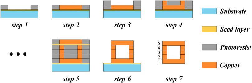
FIGURE 1. Processing steps of micro-metallic structures.
Based on this fabrication technique, Figure 2 shows the cross-section dimensions and frequency ranges of some types of possible waveguides compatible with the process. Although there are slight differences (in dimensions) between the proposed waveguides and the standard ones (due to the limitation of the standard layer thickness), the operating frequency of these waveguides can be from 220-900°GHz. In this particular work, WR-3.4/ WR-2.2 waveguides were fabricated.
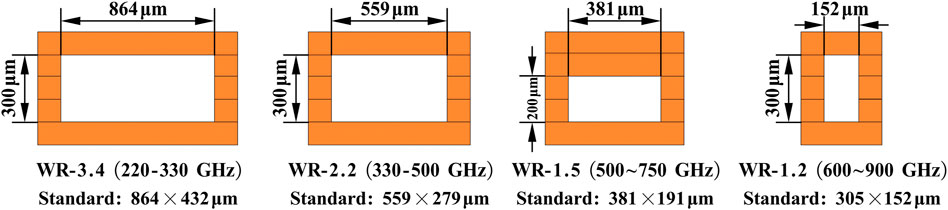
FIGURE 2. Cross-section dimensions of several types of designed rectangular waveguides range from 220-900°GHz.
The 3-D simulation model of the proposed WR-3.4 waveguide are depicted in Figure 3, and the WR-2.2 waveguide is identical to it except for the dimensions. According to the boundary condition, the current in the top/bottom wall (paralleled with x axis) can be written as [15]:
And the sidewall currents are given as:
From the equations, as long as the release holes are placed parallel to the surface current direction (in TE10 mode) and have narrow width, limited impact will be introduced by the holes and additional radiation loss can be kept in low level. However, in practical fabrication, the width of the holes cannot be set too narrow to affect the release of redundant photoresist, and it leads to an extra radiation loss, especially in high frequency parts of the ranges. As a compromise, the final dimensions of release holes walls are given in Figure 3. Compared to the situation without holes, up to extra 0.67/0.51°dB losses were observed in WR-3.4/ WR-2.2 waveguides.Hence, little radiation loss will be introduced.
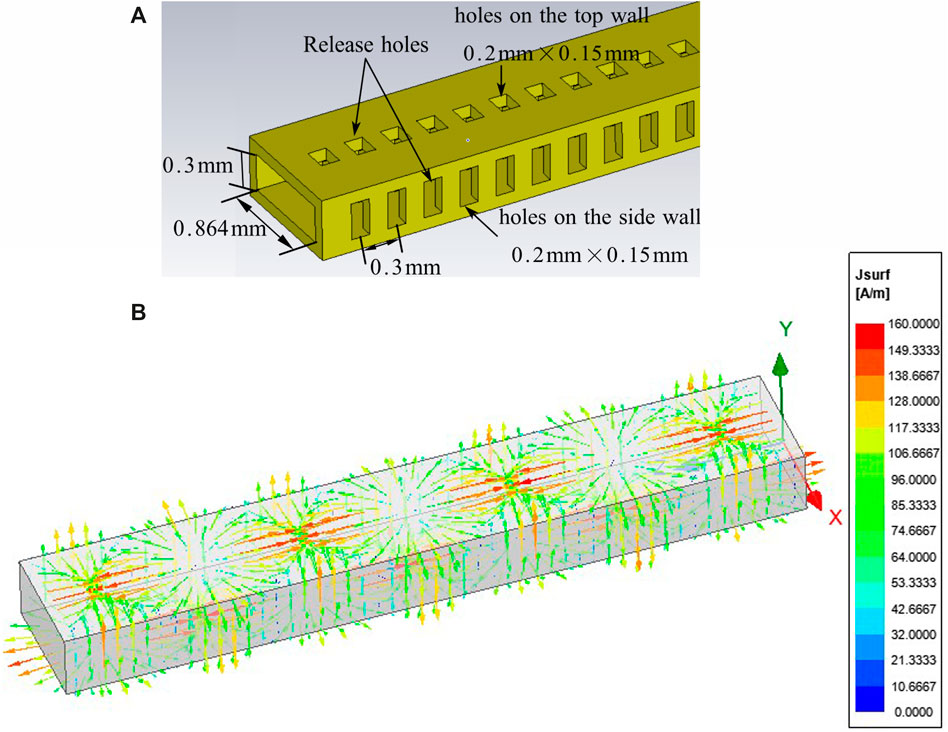
FIGURE 3. Structure of WR-3 waveguide and its surface current distribution. (A) Simulated model. (B) Current distribution
3 Considerations for measurements
In order to facilitate the measurement of the waveguides, a pair of E-plane bends were designed and four identical waveguides were placed on a single test chip as shown in Figure 4. The simulated RF performance of the bend transitions are plotted in Figure 5, showing that little impact is contributed by the bend structure on waveguide`s transmission loss.
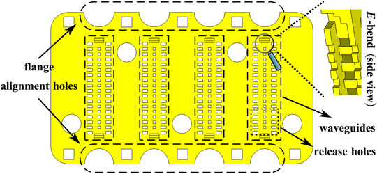
FIGURE 4. Arrangement of components on one chip.
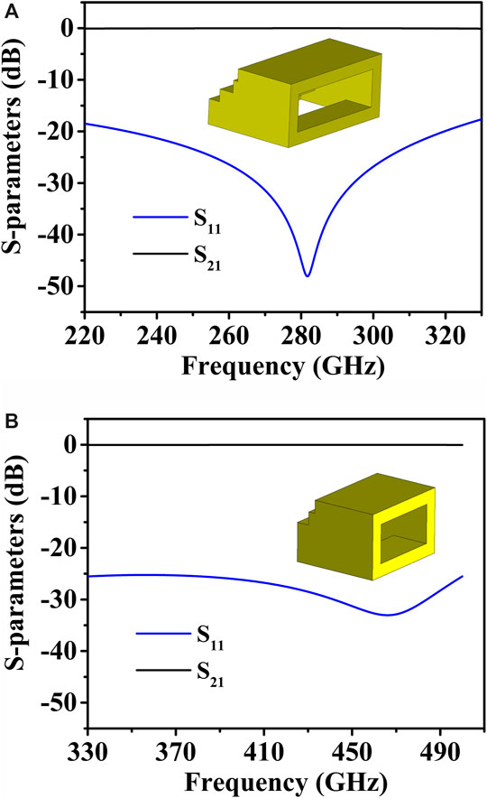
FIGURE 5. Simulated results of two bend transitions. (A) Bend used in WR-3.4 band. (B) Bend used in WR-2.2 band
In order to measure the waveguide using a conventional vector network analyser (VNA), a test fixture was designed, as shown in Figure 6. During the test, the device under test (DUT) was placed on the fixture, and the input /output ports of the DUT were aligned with the ports on the fixture through the alignment pins. In order to minimize the misalignment between the chip and the fixture, some tightly-fitting circular (on the fixture) and semi-elliptical alignment holes (on the test chip) were designed to help to improve the alignment accuracy [16]. As shown in Figure 6, through the waveguide channels inside the fixture, the DUT interfaces are extended to the flanges on both sides of the fixture. In order to calibrate the loss introduced by the fixture, another channel (between P3 and P4) was used and the length of the channel is the sum of the lengths of the two waveguide channels (between P1 and P2).
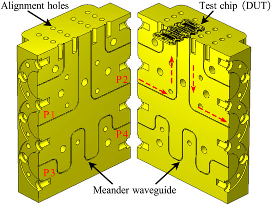
FIGURE 6. Structure of the test fixture, the red dotted arrows represent the direction of signal transmission.
4 Experimental results
In this work, some WR-3.4 waveguides with the length of 7.8°mm and WR-2.2 waveguides with the length of 6°mm were fabricated. During the measurement, the VNA was calibrated using the proposed methods in four steps: Step 1, to calibrate the loss in the fixture, the VNA was connected with the ports (P3 and P4) and a one-step through calibration was used to remove the losses from the fixture; Step 2, the VNA was connected with the ports (P1 and P2) to obtain the IL of the waveguide. Step 3, a one port calibration was carried out on P1 and Step 4, the RL of the waveguide was measured. The measured transmission and reflection coefficients were plotted in Figure 7. For ease of comparison, the theoretical losses for standard copper waveguides with same length and without surface roughness are also plotted in the figure.
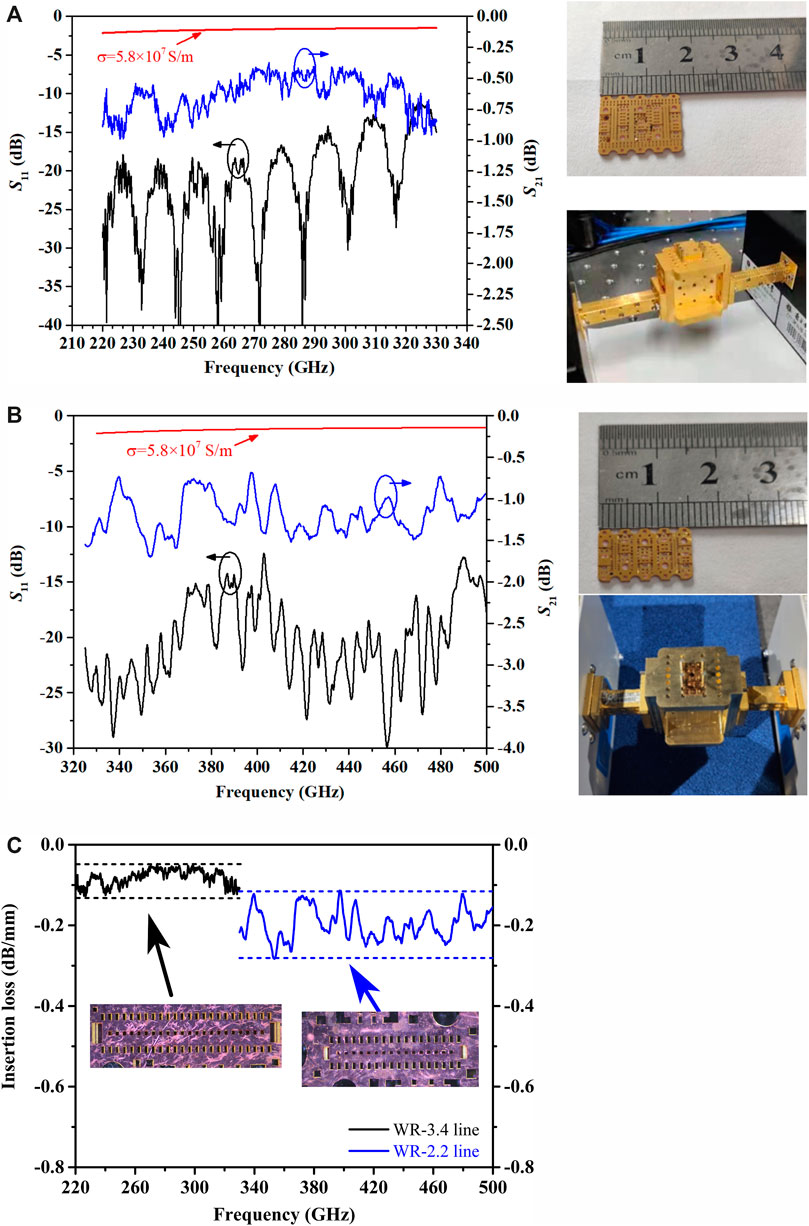
FIGURE 7. Measured results of two types of waveguides. (A) S-parameters of a WR-3.4 waveguide line with a length of 7.8°mm. (B) S-parameters of a WR-2.2 waveguide line with a length of 6°mm. (C) Insertion loss per unit length of two types of waveguides
The return loss of WR-3.4 waveguide lines is better than 12°dB across the band. The insertion loss is between 0.48°dB and 0.95°dB, and the corresponding insertion loss per unit length ranges from 0.0615°dB/mm to 0.122°dB/mm, averaging 0.098°dB/mm. As for the WR-2.2 waveguide line, the return loss is better than 13°dB in whole band, and the insertion loss is between 0.696°dB and 1.686°dB. The calculation shows that the loss per unit length can be found to be 0.116-0.281°dB/mm, averaging 0.2°dB/mm. It can be seen that the loss per unit length of WR-2.2 is about twice that of WR-3.4, even at 330 GHz. It can be explained by the different cross-section sizes of the two waveguides.
5 Discussions and considerations on surface roughness
Table 1 listed the state-of-art performance achieved by different machining technology. Indeed, the loss is comparable to that of the waveguides made by UV-LIGA and metal 3-D printing, but higher than that of the waveguide made by the SU-8 and DRIE. And this result can be explained by the higher surface roughness. SU-8 and DRIE process divide the waveguide into blocks in fabrication, and it becomes more convenient to treat most of the inner surfaces. For example, some post-treatment methods such as oxidation step (used in [6]) and chemical electroplating can be utilized to further reduce the surface roughness. However, in our work, similar to other additive manufacturing technologies, the internal surfaces can hardly be accessed for post processing. As a result, the surface roughness can be much higher in some areas. As shown in Figure 1 and Figure 8, as the waveguide was built up from the bottom (layer 1) to the top (layer 5) , the top surface of layer 1 usually has the best surface roughness (∼10°nm), because it was polished in step 2. Although the sidewalls of the waveguide cannot be planarized directly, they were defined by the lithography process hence the surface roughness of the sidewall is relatively small (in the range of 100∼300 nm). In comparison, the top surface of the waveguide (namely, the bottom face of layer 5) has the worst surface roughness (estimated to be around 1°μm), generally because this is the joint of three different materials (as seen in Step 5), namely, the seed layer, the copper and the photoresist. And apparently, it cannot be polished anyway.
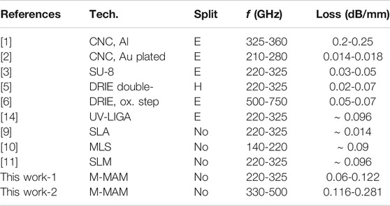
TABLE 1. State-of-the-art waveguide performance implemented with different technologies
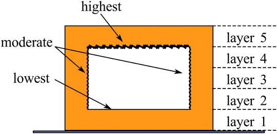
FIGURE 8. Schematic diagram of surface roughness on side walls.
6 Conclusion
The design, fabrication and measurement techniques for a set of low-loss slotted waveguides based on micro metal additive manufacturing technology has been presented for the WR-3.4 and WR-2.2 bands, respectively. The insertion loss per unit length of 0.0615-0.122°dB/mm and 0.116-0.281°dB/mm in corresponding frequency bands is achieved, verifying the feasibility of proposed methods.
Data Availability Statement
The original contributions presented in the study are included in the article/Supplementary Material, further inquiries can be directed to the corresponding author.
Author Contributions
All authors listed have made a substantial, direct, and intellectual contribution to the work and approved it for publication.
Funding
This work was supported in part by the National Natural Science Foundation of China under Grants 62001367, 61601360, 61801367, in part by the China Postdoctoral Science Foundation under Grant 2019M663715 and in in part by the NSFC of Shaanxi Province under Grants 2020JQ-076.
Conflict of Interest
The authors declare that the research was conducted in the absence of any commercial or financial relationships that could be construed as a potential conflict of interest.
Supplementary Material
The Supplementary Material for this article can be found online at: https://www.frontiersin.org/articles/10.3389/fphy.2021.696318/full#supplementary-material
References
1. Reck T, Jung-Kubiak C, Siles JV, Lee C, Lin R, Chattopadhyay G, et al. A Silicon Micromachined Eight-Pixel Transceiver Array for Submillimeter-Wave Radar. IEEE Trans Thz Sci Technol (2015) 5(2):197–206. doi:10.1109/TTHZ.2015.2397274
2. Kerr AR, Litton C, Petencin G, Koller D, Shannon M, Loss of Gold Plated Waveguides at 210-280 GHz. ALMA Memo 585 (2009).
3. Shang X, Ke M, Wang Y, WR-3 Band Waveguides and Filters Fabricated Using SU8 Photoresist Micromachining Technology. IEEE Trans Thz Sci Technol (2012) 2(6):629–37. doi:10.1109/TTHZ.2012.2220136
4.Virginia Diodes Inc. ‘Waveguide Band Designations’ (2015). Available at: http://www.virginiadiodes.com/
5. Beuerle B, Campion J, Shah U, Oberhammer J. A Very Low Loss 220-325 GHz Silicon Micromachined Waveguide Technology. IEEE Trans Thz Sci Technol (2018) 8(2):248–50. doi:10.1109/TTHZ.2018.2791841
6. Jung-Kubiak C, Reck TJ, Siles JV, Lin R, Lee C, Gill J, et al. A Multistep DRIE Process for Complex Terahertz Waveguide Components. IEEE Trans Thz Sci Technol (2016) 6(5):1–6. doi:10.1109/TTHZ.2016.2593793
7. Guo C, Dhayalan Y, Shang X, Powell J, Lancaster MJ, Xu J, et al. A 135-150-GHz Frequency Tripler Using SU-8 Micromachined WR-5 Waveguides. IEEE Trans Microwave Theor Techn. (2020) 68(99):1035–44. doi:10.1109/TMTT.2019.2955684
8.Kayaku Advanced Materials, Inc. “SU-8 2000 Permanent Epoxy Negative Photoresist,” Microchem, Tech Rep (2019). Available at: https://kayakuam.com/wp-content/uploads/2019/09/SU-82000DataSheet2100and2150Ver5.pdf
9. Bieren AV, Rijk ED, Ansermet JP, Macor A. Monolithic Metal-Coated Plastic Components for Mm-Wave Applications. 39th Int Conf Infrared, Millimeter, Terahertz waves (2014):1–2. doi:10.1109/IRMMW-THz.2014.6956222
10. Fiorese V, Goncalves CB, del Rio Bocio C, Titz D, Gianesello F, Luxey C, et al. Evaluation of Micro Laser Sintering Metal 3D-Printing Technology for the Development of Waveguide Passive Devices up to 325 GHz. IEEE/MTT-S Int Microwave Symp (Ims) (2020):1168–1171. doi:10.1109/IMS30576.2020.9224102
11. Zhang B, Zirath H. Metallic 3-D Printed Rectangular Waveguides for Millimeter-Wave Applications. IEEE Trans Compon., Packag Manufact Technol (2016) 6(5):796–804. doi:10.1109/TCPMT.2016.2550483
12. Chattopadhyay G, Reck T, Lee C, Jung-Kubiak C. Micromachined Packaging for Terahertz Systems. Proc IEEE (2017) 105(2.176):1139–50. doi:10.1109/JPROC.2016.2644985
13. Li H, Li Y, Feng J. Fabrication of 340-GHz Folded Waveguides Using KMPR Photoresist. IEEE Electron Device Lett (2013) 34(3):462–4. doi:10.1109/LED.2013.2241389
14. Stanec JR, Barker NS. Fabrication and Integration of Micromachined Submillimeter-Wave Circuits. IEEE Microw Wireless Compon Lett (2011) 21(8):409–11. doi:10.1109/LMWC.2011.2158411
Keywords: Waveguide, micro metal additive manufacturing, low-loss slotted waveguide, millimeter wave measurement, micromachining
Citation: Wu Z, Shi G, Yu Y, Wen X, Guo C and Zhang A (2021) Micro Metal Additive Manufactured Low-Loss Slotted Rectangular Waveguides Operating at 220-500 GHz. Front. Phys. 9:696318. doi: 10.3389/fphy.2021.696318
Received: 16 April 2021; Accepted: 07 May 2021;
Published: 27 May 2021.
Edited by:
Gang Zhang, Nanjing Normal University, ChinaReviewed by:
Jiayu Rao, Heriot-Watt University, United KingdomGuoxiang Shu, Shenzhen University, China
Copyright © 2021 Wu, Shi, Yu, Wen, Guo and Zhang. This is an open-access article distributed under the terms of the Creative Commons Attribution License (CC BY). The use, distribution or reproduction in other forums is permitted, provided the original author(s) and the copyright owner(s) are credited and that the original publication in this journal is cited, in accordance with accepted academic practice. No use, distribution or reproduction is permitted which does not comply with these terms.
*Correspondence: Cheng Guo, spmguo@163.com
†These authors have contributed equally to this work and share first authorship