Templating Functional Materials Using Self-Assembled Block Copolymer Thin-Film for Nanodevices
 Ashwanth Subramanian
 Nikhil Tiwale
 Won-Il Lee
 Chang-Yong Nam
- 1Department of Materials Science and Chemical Engineering, Stony Brook University, Stony Brook, NY, United States
- 2Center for Functional Nanomaterials, Brookhaven National Laboratory, Upton, NY, United States
The nanomorphologies and nanoarchitectures that can be synthesized using block copolymer (BCP) thin-film self-assembly have inspired a variety of new applications, which offer various advantages, such as, small device footprint, low operational power and enhanced device performance. Imperative for these applications, however, is the ability to transform these small polymeric patterns into useful inorganic structures. BCP-templated inorganic nanostructures have shown the potential for use as active materials in various electronic device applications, including, field-effect transistors, photodetectors, gas sensors and many more. This article reviews various strategies that have been implemented in the past decade to fabricate devices at nanoscale using block copolymer thin films.
Introduction
Increasing amount of the cost associated with lithography-based top-down patterning and its complexity has slowed down the aggressive downscaling of semiconductor devices that has been continuing for the past several decades, essentially ending the Moore’s law era. Self-assembled block copolymer (BCP) thin films have emerged as a nontraditional material patterning process because of their ability to spontaneously generate various nanopatterns, providing several advantages including reduction in material and processing cost, small feature size (<30 nm) not easily achievable by traditional lithographic processes, and ability to be easily incorporated into existing technology for large-scale manufacturing. However, BCP nanopatterns are not directly useful for many applications because of their limited material properties inherent to polymers. For instance, poly (styrene-block-methyl methacrylate) (PS-b-PMMA) BCP thin film, which has been extensively studied for material nanopatterning, has poor mechanical, thermal and electrical properties compared to their inorganic counterparts, making them unsuitable for direct device application. Typically, post-self-assembly processing will be required in order to transform these polymeric patterns into more useful inorganic nanostructures. This review article summarizes various strategies that have been used in creating functional nanostructures templated by BCP thin films for nanoelectronic devices.
Block Copolymer Derived Strategies for Nanodevice Fabrication
Plethora of research has been conducted over the past 2 decades in studying various morphologies formed by self-assembly of BCP structures with two or more number of polymer blocks linked together and has been summarized in recent reviews. (Segalman, 2005); (Hu et al., 2014); (Tseng and Darling, 2010) A typical diblock BCP consists of two immiscible polymeric chains/blocks that are covalently bound to each other at one end. In the molten state, hydrophilic and hydrophobic domains of the BCP are driven to undergo phase separation due to repulsion between these immiscible blocks. Such repulsive forces act until the unfavorable interaction between the BCP domains is minimized and reach equilibrium forming different nanomorphologies. Such a phase separation is controlled by the Flory-Huggins Interaction parameter (χ), composition or volume fraction (f) and degree of polymerization or molecular weight of the blocks (N). Mathematically, the free energy for the self-assembly process can be approximately expressed by the Flory-Huggins equation:
Where, A and B represent the two polymeric blocks,
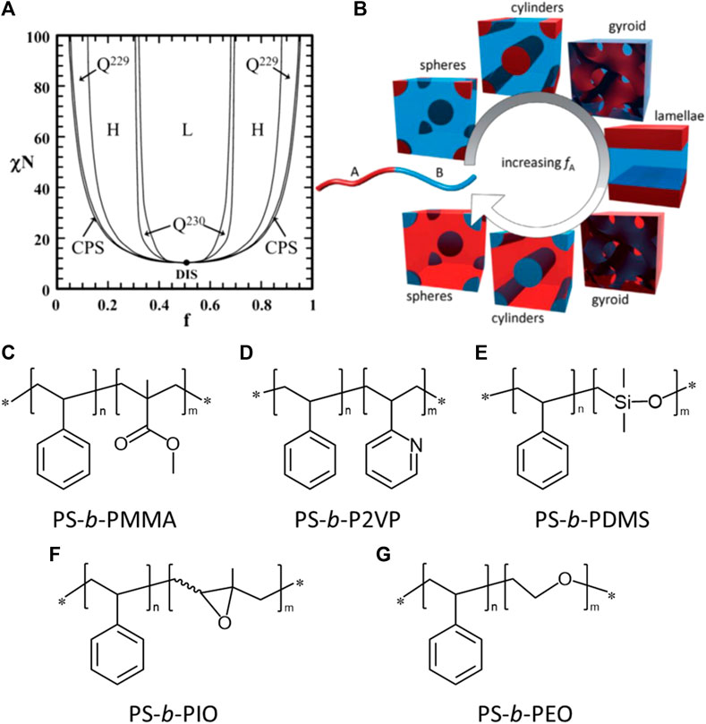
FIGURE 1. (A) Phase diagram of PS-b-PMMA system, indicating regions of interaction parameter (χ) and volume fraction (f) that give rise to formation of different morphologies where L: lamellae, H: hexagonally packed cylinders, Q230: double gyroid phase, Q229: body-centered spheres, CPS: closed-packed spheres, and DIS: disordered phase (B) represents evolution of different morphologies as volume fraction of component A is increased. (Reproduced from ref. 1) (C–G) chemical structures of various commonly used block copolymers that are addressed throughout this manuscript.
In general, a vast majority of exploration in the domain of BCP thin film self-assembly has been focused on systems containing primarily dielectric polymer-blocks, such as PS-b-PMMA, poly (styrene-block- vinyl pyridine) (PS-b-PVP), poly (styrene-block-dimethylsiloxane) (PS-b-PDMS). In order to utilize BCP-based nanostructures for functional device applications, modifying these morphologies to exhibit conducting, semiconducting and/or optical properties is necessary. (Kim et al., 2010) Here we outline some of the modification routes that have been implemented so far for fabricating such nanodevices.
Thin Film Deposition-Based Pattern Transfer
One of the straightforward methods to convert BCP patterns into electrically active structures is by lift-off process. In a typical lift-off process, a thin film of required material is deposited onto a substrate with polymeric patterns and subsequently, the part of the deposited film residing on the polymer is washed off when the polymer is dissolved in suitable solvent. He and Stoykovich et al. have demonstrated a simple approach to generate undercut sidewall profile necessary for lift-off by two-step BCP self-assembly, where the top layer is assembled with same periodicity but slightly smaller PMMA domain width (Figure 2A). (He and Stoykovich, 2014) By blending thermally cross-linkable homopolymers with BCP, the composition is appropriately tuned to self-assemble the two BCP layers successively, with thermal crosslinking freezing the structures after each self-assembly. The PMMA domain of the self-assembled films, after subjecting to the ultraviolet (UV) light (λ= 254 nm; 1 Jcm−2), then can be selectively removed by developing in acetic acid and descumming leftover residue by short oxygen plasma (Figure 2B). Subsequently, 5 nm of Au was deposited with 1 nm of Cr adhesion layer by thermal evaporation (Figure 2C). The PS layer along with the metal deposited on it were removed by lift-off process by submerging the samples in 55°C toluene solution along with ultrasonic agitation to obtain Au fingerprint nanowires (Figure 2D) templated by the PMMA domain of the BCP. This strategy in general can be extended to achieve patterns of functional metallic or semiconducting materials, and can be extended to use other sacrificial layers. (He and Stoykovich, 2014)
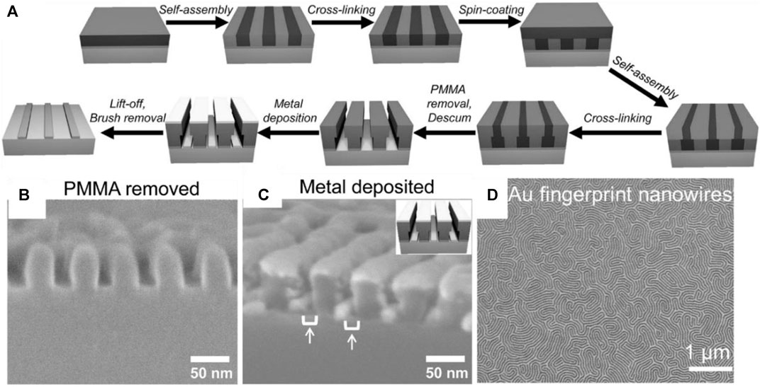
FIGURE 2. (A) Schematic process flow of the lift-off based fabrication of Au nanowire network with lamellar block copolymer thin film as template; Cross-sectional scanning electron microscopy (SEM) micrograph of PS-b-PMMA bilayer (B) after selective PMMA removal and (C) after the thermal deposition of Cr/Au thin film; (D) Top-view SEM of the fingerprint templated Au nanowire network after lift-off. Reproduced with permission from ref (He and Stoykovich, 2014).
Meanwhile, it is important to consider that the transport behavior is dependent on the BCP thin film topology and length scale over which the nanostructures are connected or percolated. The long-range spatial arrangement, interconnected domains and defects within the morphology of the BCP thin films can be together termed as “network topology”. To achieve reproducibility among the nanoscale devices, it is of paramount importance to minimize these defects. In particular, the lamellar morphology, which typically exhibits lack of long-range order because their inter-domain interface are directed perpendicular to the substrate, has been found to form highly curved, tortuous, and intermixed domains. Stoykovich and coworkers have previously reported that the compositional symmetry (commonly referred to as block ratio) of the PS-b-PMMA BCP thin films can impact the continuity over long-range and the degree of connectedness within the network when self-assembled in lamellar morphology. (Campbell et al., 2012); (Diederichsen et al., 2015) Particularly, the fingerprint pattern generated by a symmetric BCP system (i.e., PS:PMMA = 50:50) does not show a long-range connectivity within the network (i.e., limited percolation). A longer-range order could be obtained by introducing structural defects that promote interconnectedness (e.g., branching and nodes) among the domains. It is possible to obtain long-range percolating networks in either the PS or PMMA domain of PS-b-PMMA BCP by increasing volume fraction of the respective block compared to the other, while making sure that the BCP still forms lamellar morphology even with the asymmetric block ratio. For example, with a PMMA volume fraction (fPMMA) of 0.45 or 0.55, the asymmetric PS-b-PMMA is able to exhibit percolating networks in the PS or PMMA domains, respectively (Figure 3A). For instance, Diederichsen and Stoykovich et al. demonstrated the fingerprint-patterned gold nanowires obtained by metal deposition and lift-off process (Figures 3B,C) using PS-b-PMMA with an asymmetric block ratio (48:52) with a long range network connectivity (as long as 500 μm) and the electrical conductance between ∼10–3–10−5 S, when the channel length was varied between 2 and 100 μm (Figure 3D). Such a defect engineering may be crucial to control BCP network topology and make them more suitable for electronic device fabrication. An alternate route to engineering defects can also be achieved by homopolymer blending into symmetric BCP systems. (Doerk and Yager, 2017; Doerk et al., 2020)
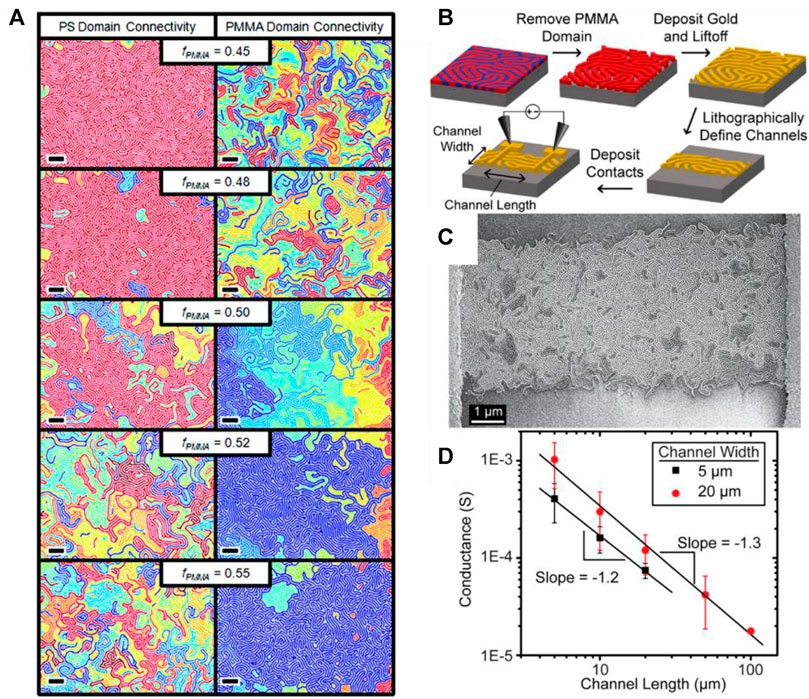
FIGURE 3. (A) Percolation network of PS (left column) and PMMA (right column) as the volume fraction of PS-b-PMMA is varied. It can be noted that when the PMMA volume fraction is decreased connected network spread in the PS domain is increased and vice versa. All the scale bars represent 400 nm; (B) Schematic showing the process flow for fabrication of device containing BCP derived nanowire networks formed by metal lift-off; (C) Scanning electron micrograph of a two-terminal device (10 μm channel length, 5 μm channel width) fabricated via BCP templated Au network; (D) Conductance variation with channel length for the BCP templated Au nanowire networks using PS-b-PMMA (fPMMA = 0.52) for channel widths of W = 5 and 20 μm. Reproduced with permission from ref (Campbell et al., 2012); (Diederichsen et al., 2015).
Alternatively, directed self-assembly (DSA) of BCP thin films can be used to overcome such defects. DSA typically enables the BCP assembly to be guided into the desired long-range order and morphology with the help of templates known as guiding patterns (GPs). GPs are normally fabricated by top-down techniques. In the case of chemoepitaxy, a neutral substrate is converted into chemical patterns exhibiting preferential wetting for one of the two BCP domains. The surface free energy of a neutral surface, can be selectively altered in number of different ways, including oxygen plasma treatement, (Oria et al., 2013), photolithography, (Cheng et al., 2010), electron-beam lithography (EBL) (Evangelio et al., 2019); (Laura et al., 2015) and scanning-probe lithography. (Gottlieb et al., 2020) During graphoepitaxy, three-dimensional (3D) topographic features are patterned on the substrate, such as trenches or holes, and the constraint employed by them on the BCP films is exploited for DSA. It is possible to tailor the physical geometry and dimension of the patterned topographies, while also chemically modifying their surface characteristics (i.e., bottom and walls) to selectively govern their affinity towards each BCP domain, thus in effect orienting their self-assembly. A more detailed account on DSA and its applications has been reported elsewhere. (Pinto-Gomez et al., 2020) Using such strategies has been useful for patterning well-ordered, defect-free nanostructures and fabricate functional devices. Jung and Ross et al. employed DSA to pattern highly ordered semiconducting polymer nanowire-based gas sensor. (Jung et al., 2008) First, silica-coated silicon substrate was patterned with trenches (40 nm deep with 1.3 μm periodicity). The patterned substrate was then sequentially coated with poly (3,4-ethylenedioxythiophene):polystyrene sulfonate (PEDOT:PSS), SiO2, and poly (dimethylsiloxane) (PDMS) homopolymer brush. Afterward, PS-b-PDMS (PS matrix, PDMS in-plane cylinders) BCP was spin-cast and self-assembled within the pre-patterned trenches with PDMS cylinders horizontally aligned along the trench length and parallel to the substrate. Exploiting these PDMS cylinders as an etching mask, the pattern was transferred to the underlying PEDOT:PSS layer using reactive ion etching process (30 s, 50 W, O2/He) obtaining PEDOT:PSS nanowires (width = 15 nm, height = 20 nm) (Figures 4A,B). To investigate the gas sensing capability of these polymer nanowires, a two-terminal device was fabricated (Figure 4C) across the PEDOT:PSS nanowires as a conductive channel (length = 1 mm, width = 1 μm) for sensing ethanol vapor. Figure 4D shows the response of the polymer sensor device as the ethanol concentration was varied using N2 carrier gas. Increasing the partial pressure of ethanol increased the sensor response. (Jung et al., 2008)
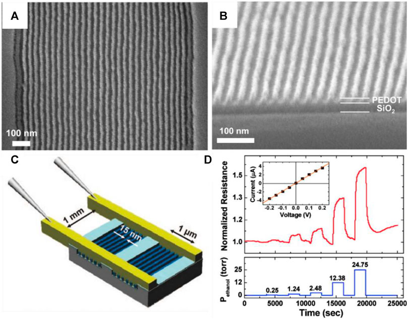
FIGURE 4. SEM micrographs of (A) Top-view and (B) cross-sectional view of PEDOT:PSS nanowires fabricated using the PS-b-PDMS DSA patterns as RIE etch mask.; (C) Schematic of a PEDOT:PSS nanowire based chemoresistive ethanol sensor; (D) The response of the nanosensor to different ethanol concentrations. Reproduced with permission from ref (Jung et al., 2008).
Metal nanodot arrays can be fabricated by lift-off process, starting with cylinder forming PS-b-PMMA and removing the PMMA domain selectively to create PS hole matrix. Following up with metal-deposition and lift-out process (to remove the PS matrix), metal nanodot arrays can be obtained. Shin and Kim et al. have demonstrated a arrays of silver nanodots used in biosensors by leveraging the tunable localized surface plasmon resonance to detect various biomarkers for diseases. (Shin et al., 2010) Xiao and Nealy et al. patterned well-ordered cobalt nanodot arrays by combining with DSA for potential applications in magnetic storage media. (Xiao et al., 2005)
A major disadvantage of the metal depositions process is that stringent control over the deposition process is needed otherwise metal lift-out would not succeed. This problem can be addressed by milling the deposited thin film by using Ar sputter etching process to remove unwanted material deposited and obtain uniform metal nanodot arrays. Barrera and coworkers, for instance, have realized defect-free magnetic nanodot arrays of NiFe alloy and Co. using sputter deposition followed by oblique 45°-Ar milling. (Barrera et al., 2017) Lin and Gladfelter et al. performed ALD of ZnO on the PS matrix and removed the PS template by thermal anneal to obtain ZnO nanocrucibles. The nanocrucibles were further filled with permalloy using evaporation. By controlling the ZnO nanocrucible and permalloy nanodot dimensions, the magnetic properties of the system could be tuned. (Lin et al., 2015) Lee and Ross et al. exploited the chemical contrast to directly deposit Cu selectively on the PS domain of self-assembled PS-b-PMMA. By carefully controlling rate of sputtering (0.016 nm/s) and for a very thin film of ∼3 nm, they grew ultra-thin copper nanomesh thin films on top of the BCP film. (Lee et al., 2021) Such thin coatings on polymers can serve as an ultra-thin coatings for various hybrid sensor device applications.
Resistive random-access memory (RRAM), an emerging class of non-volatile memory, are plagued by random formation and rupture of conductive filaments, resulting in poor device performance. Frascaroli and Spiga et al. have demonstrated high density HfO2-based RRAM devices by patterning the Ti/Pt top electrode using metal lift-out process. The templated top electrode reduced the active device dimension to as low as 28 nm and fabricated up to 5 × 10¹⁰ devices/cm (Black et al., 2007). (Frascaroli et al., 2015) You and Lee et al. showed that by decorating the top surface of the switching medium using silica nanodots templated by self-assembled PS-b-PDMS BCP, they observed reduction in standard deviation in the set and reset voltage from ∼77 to ∼60%, thus improving the device repeatability and reproducibility. (You et al., 2014)
Vapor-Phase Infiltration of Functional Materials
Another way to convert BCP patterns into inorganic nanostructures is by infiltration synthesis, a material hybridization technique which is guided by the dissolution, diffusion and reaction of metal precursors with polymer templates. (Waldman et al., 2019a); (Leng and Losego, 2017) The infiltration process can be classified, based on the type of precursors used, to vapor-phase infiltration (VPI) and liquid-phase infiltration. These techniques enable the growth of inorganic materials within an organic polymer matrix, creating an organic-inorganic hybrids. Such hybrids typically display superior material properties by combining the individual starting components at molecular level. VPI, which is also referred to as sequential infiltration synthesis (SIS), has been demonstrated for enhancing various properties of polymers such as mechanical, (Dusoe et al., 2017); (Lee et al., 2009); (Lee et al., 2010); (Gregorczyk et al., 2015) chemical, (Tseng et al., 2011; TsengTseng et al., 2011; McGuinness et al., 2020), electrical, (Nam et al., 2015a; Subramanian et al., 2019), optical, (Rahman et al., 2014; Rahman et al., 2015; Ocola et al., 2016), triboelectric, (Yu et al., 2015; Yu and Wang, 2016), and thermal properties. (Bamford et al., 2021) These hybrids have been useful for a wide variety of applications (Subramanian et al., 2018); (Berman and Shevchenko, 2020) such as gas separation, (Greil et al., 2017), oil absorption, (Barry et al., 2017), photodetectors, (Nam and Stein, 2017), gas sensors, (Pleshek et al., 2021), energy conversion. (Yu et al., 2015) and filteration. (Zhou et al., 2017) An important application of VPI generated hybrids has been in material nanopatterning, where patterned polymer templates can be either directly converted into electrically functional nanostructures (Peng et al., 2011; Nam et al., 2015b) or by transferring the pattern to an underlying substrate that can be incorporated into existing nanoelectronic device architecture. (Peng et al., 2010; TsengTseng et al., 2011)
Typical process steps required to convert organic BCP to inorganic nanopatterns by infiltration synthesis are driven by the interaction between functional groups in BCP and the physio-chemical properties of metal precursors. For instance, in the case of the SIS in PS-b-PMMA, organometallic precursor trimethylaluminum (TMA) selectively reacts and binds to the carbonyl/ester groups in the PMMA block enabling growth of aluminum oxide (AlOx) selectively within the PMMA domain of the BCP. Post-infiltration polymer ashing steps can be used to selectively remove the organic BCP matrix and generate inorganic nanostructures templated by BCP. The combined strategy of BCP self-assembly followed by SIS has been widely reported for fabricating AlOx nanostructures, such as nanowires (fingerprint pattern), (Peng et al., 2011), nanoholes, (Kamcev et al., 2013), and nanodots, (Liapis et al., 2017), with controllable feature size (<30 nm). It is possible to control the size of AlOx nanowires from 8 to 30 nm by controlling the number of SIS cycles (from 1 to 10) into the self-assembled PS-b-PMMA thin films. (Peng et al., 2010)
While extensive research has been conducted to understand and optimize AlOx patterning using BCP, AlOx is electrically insulating and show negligible optical activity in the visible wavelength range, making it unsuitable for application in functional devices. Patterning more functional materials such as zinc oxide (ZnO), tin oxide (SnOx), titanium dioxide (TiO2), aluminum doped ZnO (AZO) can be useful for various device applications, such as optochemical sensors, field-effect transistors (FETs), energy harvesting device, and this can be achieved by modifying the patterned BCP template with additional processing steps to assist the infiltration of functional materials. The PMMA matrix, which is weakly interacting with material precursors such as diethyl zinc (DEZ), SiCl4, and WF6, can be initially subjected to a more reactive TMA and subsequently converted to AlOx to generate -Al-CH3 and -Al-OH reactive sites. Such a “priming” step may consist of ∼one to three AlOx infiltration cycles and can be effective in enhancing reactivity of PMMA block for infiltrating various other materials such as ZnO, SiO2, TiO2, and W (Figure 5A–D). (Peng et al., 2010; Peng et al., 2011)
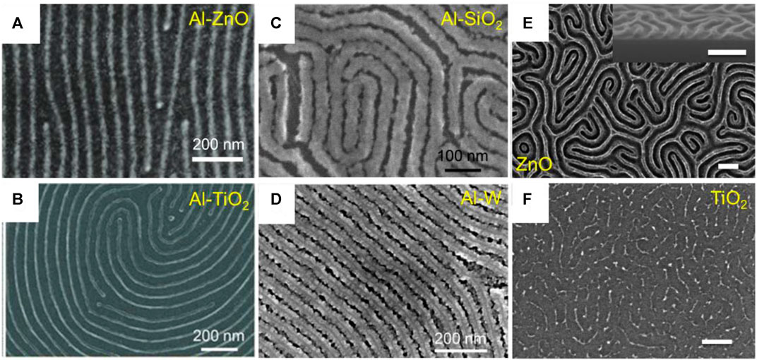
FIGURE 5. a) SEM micrographs of infiltration-synthesized Al primed (A) ZnO; (B) TiO2; (C) SiO2; (D) W; SEM images of (E) ZnO; and (F) TiO2 nanowires obtained via infiltration into the PS domain of UV/O2 modified PS-b-PMMA BCP film. Reproduced with permission from ref (Subramanian et al., 2019).
Chemical modification of the self-assembled PS-b-PMMA templates also has shown to enable the SIS of ZnO, TiOx, and AlOx into the PS domain, instead of the PMMA domain, fabricating the inverse morphology compared to the one fabricated via standard SIS. UV irradiation can be used to initiate photooxidation of the PS block in the presence of small quantity (<5%) of oxygen, and the resulting decomposition of phenyl rings of PS domain results in various chemical moieties such as hydroxyl, carboxyl, carbonate, and carbonyl groups that can impart elevated Lewis basicity to the PS domain and hence enhance reactivity towards organometallic precursors that otherwise exhibit weak reactivity. On the other hand, ester groups in the PMMA domain are degraded into weakly reactive saturated C-C bonds due to UV exposure, inhibiting the SIS into PMMA block. Using this strategy, Kamcev and Nam et al., demonstrated the fabrication of ZnO, TiOx, and AlOx nanomorphologies replicating the PS domain (Figure 5E,F) without requiring AlOx priming. (Kamcev et al., 2013) Over the years, other functional materials such as SnOx, GaOx, InOx have also been successfully patterned using PS-b-PMMA templates. (Waldman et al., 2019b).; (Barun, 2019)
While post-self-assembly modification strategies are indeed useful to obtain functional inorganic nanostructures templated by BCP, such processing steps can influence the electrical properties of the functional materials. For instance, alumina priming process applied for the ZnO infiltration into PS-b-PMMA can influence the conductivity of the final ZnO nanowires obtained since aluminum acts as a dopant. (Luka et al., 2011) Therefore direct infiltration of ZnO is essential to obtain ZnO nanostructures with intrinsic ZnO properties. One possible way to directly infiltrate electroactive materials is the utilization of a more reactive BCP system, such as PS-b-(poly (2-vinylpyridine)) (PS-b-P2VP) where precursor interaction with P2VP is much stronger due to the presence of more Lewis-basic pyridine group in the P2VP domain. (Kamcev et al., 2013; Chai et al., 2007; Chai and Buriak, 2008) Subramanian and Nam et al. reported a strategy to directly pattern ZnO nanowires templated by PS-b-P2VP by implementing a modified SIS protocol called “microdose” process in which the infiltrated DEZ/H2O precursor concentration was increased by multiple precursor pulses along with increased exposure time to finally yield a uniform ZnO infiltration into the P2VP domain, leading to high-fidelity pure ZnO nanowire patterns. (Subramanian et al., 2019) Conformal surface coating of thin TiOx layer via atomic layer deposition (ALD) before annealing the wires helped retain the structural integrity of the ZnO nanowires templated by BCP (Figure 6A) and was critical to realize optoelectronically active ZnO nanostructures. (Subramanian et al., 2019)
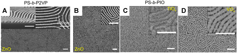
FIGURE 6. (A) SEM micrographs depicting ZnO nanowire patterns synthesized via microdose-infiltration-synthesis into self-assembled PS-b-P2VP. Reproduced with permission from ref (Subramanian et al., 2019) SEM micrographs of (B) ZnO; (C) TiOx; and (D) VOx synthesized via infiltration into PS-b-PIO. Reproduced with permission from ref (Yi et al., 2019).
Similarly, Yi and Grubbs et al. reported that various functional metal oxides can be directly fabricated by performing infiltration into polystyrene-block-poly (epoxyisoprene) (PS-b-PIO). In this BCP, the PIO block contains a reactive epoxy ring, making it a strong Lewis base, to which vapor-phase metal precursors can directly react and bind. Using this BCP system, diverse metal oxide nanostructures, including AlOx, ZnO, TiOx and VOx were obtained (Figures 6B–D). (Yi et al., 2019)
In addition, the BCP self-assembly process can be combined sequentially with the VPI process to generate complex, 3D inorganic nanostructures potentially useful for electronic device applications. Recursively stacked BCP self-assembly can generate 3D nanomesh structures exploiting the orthogonal self-alignment of the BCP layers starting with either lithographically patterned trenches or dots (Amir Tavakkoli et al., 2016) or BCP templated nanostructures. (Rahman et al., 2016) Spontaneous orthogonal alignment of BCP thin films can be attributed to the polymer chain stretching or compression causing entropic energy penalty when lamellar BCP domains align in parallel with the underlying corrugation. (Carpenter et al., 2017); (Han et al., 2010) Metal oxide thin-film nanoarchitectures can also be realized by combining VPI with spontaneous orthogonal self-alignment of successively stacked lamellar BCP patterns. The spontaneous orthogonal alignment process can be easily applied to a large area by using simple starting templates that do not require specially engineered substrates or complicated pre-processing. In addition, it also enables inter-layer electrical network connections across the stacked nanowire layers. Subramanian and Nam et al. reported the realization of 3D ZnO nanomesh by successively stacking controlled number of ZnO nanowire layers templated by BCP (Figures 7A–C). (Subramanian et al., 2019) Electrical conductivity across the multilayered nanomesh was observed to depend on the number of patterned layers. If enough layers are stacked, geometrical 3D charge percolation conduction is established across overlapping and orthogonal staking of nanowire fingerprint sublayers (Figure 7D). For this reason, these systems represent percolative conduction networks where conductivity can be controlled by properly tuning geometrical parameters of the metal oxide nanostructures. Also demonstrated was opto-electrical response of the nanomesh structures with a ∼three-order increase in electrical conductance upon exposure to UV light, which not only directly excites charge carriers but also assists the desorption of chemisorbed surface oxygens, yielding a photo-gain effect (i.e., additional mobile charge carrier generation). (Nam and Stein, 2017) As a perspective, nanoarchitectures with tailored conductance properties can be realized by exploiting and combining different BCPs patterning strategies and making them suitable for different chemical and optical sensor applications. (Rahman et al., 2016)
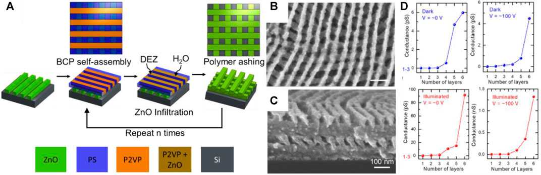
FIGURE 7. (A) Schematic description of ZnO nanomesh structure fabrication procedures exploiting recursive spontaneous orthogonal alignment of lamellar BCP; SEM micrographs illustrating (B) Top-view and (C) Cross-sectional view of 4-layer ZnO nanomesh; (D) differential conductance of ZnO nanomesh with respect to the number of ZnO nanowire layers at: (left) V = 0 V and (right) V = 100 V. Reproduced with permission from ref (Subramanian et al., 2019).
Liquid-Phase Infiltration of Functional Materials
The liquid-phase infiltration (LPI) process uses inorganic salt solutions that can be prepared by dissolving the salts in water or suitable organic solvents. The infiltration is enabled by direct interaction between the inorganic elements in the form of aqueous metallic ions (cations, anions or coordinated complex ions) and reactive functional groups in the BCP template by simply immersing polymeric templates into the inorganic salt solution without the need of specialized equipment. (Aizawa and Buriak, 2006; Chai et al., 2007; Majewski et al., 2015) For example, the infiltration of various metallic elements, including Al, Hf, W, Fe, Mo, Cu, Ce, Pb, Pd, Ti, and Zr, into the BCP systems such as (PS-b-P2VP) [or poly (4-vinylpyridine) (P4VP)] and PS-b-poly (ethylene oxide) (PS-b-PEO) has been demonstrated to synthesize BCP-templated hybrid films and directly patterned inorganic nanostructures. (Chai and Buriak, 2008; Cummins et al., 2016); (Cummins et al., 2013); (Cummins et al., 2015); (Varghese et al., 2013); (Ghoshal et al., 2012); (Ghoshal et al., 2016).; (Shin et al., 2013)
Buriak and coworkers have previously hypothesized the mechanism of precursor infiltration into PS-b-P2VP and PS-b-P4VP BCP thin film templates. The P2VP and P4VP blocks are perceived to exhibit the ability to form complex coordinate bonds with infiltrating metallic precursors due to the presence of the Lewis-basic pyridine group (Lewis basicity, pKb, ∼6); when exposed to an acidic metal salt solution, the basic pyridine group undergoes protonation by donating the lone pair of electrons on the nitrogen atom (not involved in the pyridine ring conjugation) and binding with positively charged H+/hydronium (H3O+) ions to form a positively charged pyridinium ion (i.e., conjugate acid of pyridine). Subsequently, negatively charged metal complex species present in the solution (e.g., tetrachloroplatinate (PtCl42–) for Pt infiltration) can electrostatically bind with the pyridinium ion, forming a Lewis acid-base adduct, leading to the selective metal loading and confinement within the P2VP (or P4VP) domain of the BCP template. (Aizawa and Buriak, 2006; Chai et al., 2007; Chai and Buriak, 2008) A similar mechanism holds true for PS-b-PEO, where the metal precursor bind to PEO. Inorganic nanostructures via LPI are synthesized by selectively removing the remaining organic component of the inorganic-infiltrated self-assembled BCP hybrid thin films and leading to their direct conversion to inorganic nanostructures that replicate the starting BCP template. This conversion is in general associated with organic mass loss and volume shrinkage, (Subramanian et al., 2020), and the amount of inorganic infiltration into the polymeric film naturally determines the quality of the converted inorganic nanostructures. (Subramanian et al., 2019)
Metal precursor infiltration during the LPI process takes place through the top surface of P2VP domain of the self-assembled PS-b-P2VP thin film, unlike the VPI process in which the infiltration of vapor-phase precursors can occur through the top surface of active domain as well as the neighboring inert BCP domain due to the fast diffusion of precursors through them without any interaction. (Subramanian et al., 2020) Thus, confinement of the infiltrated metal ions at the surface regions of P2VP domain can result in discontinuous nanostructures after conversion to inorganic that are unsuitable for any device application. Additionally, various reports have shown that LPI, when performed at room-temperature conditions, generally requires prolonged soaking times (1–24 h) to infiltrate enough quantity of inorganic entities into BCP templates to obtain high-fidelity inorganic nanostructures upon conversion. Since it is well known the infiltration of inorganic materials into organic polymer systems is dependent on the balance between two competing fundamental processes: 1) dissolution of inorganic precursors into the polymer matrix and 2) the subsequent binding reaction between the precursor and the reactive functional groups available within the polymer matrix, (Richard, 2014), LPI performed at elevated temperatures accelerates the diffusion kinetics of infiltrating ions and enhances the extent of LPI. By performing LPI at elevated temperatures (i.e., heated LPI; between 20 and 80°C), Subramanian and Nam et al. have demonstrated tunability of Pt nanowire dimensions by controlling the infiltration temperature and soak times (Figures 8A,B). The Pt nanowires synthesized by the temperature-enhanced LPI process well replicated the lamellar pattern of starting self-assembled PS-b-P2VP with controllable nanowire size and cross-sectional shape (line width between 8 and 25 nm; height between 5 and 40 nm), enabling a versatile, high-fidelity pattern transfer. Furthermore, in order to demonstrate the electrical functionality of Pt nanostructures, heated LPI was combined with spontaneous orthogonal alignment of subsequent BCP nanowire layers to obtain multi-layered Pt nanomesh architectures (Figures 8C,D). The Pt nanomesh architectures featured a 3D percolating electrical conductance that was dependent on the number of nanowire stack layers (1–7 layers) which resulted in five-order tunability of the sheet conductance between ∼10−2–103 S (Figure 8E).
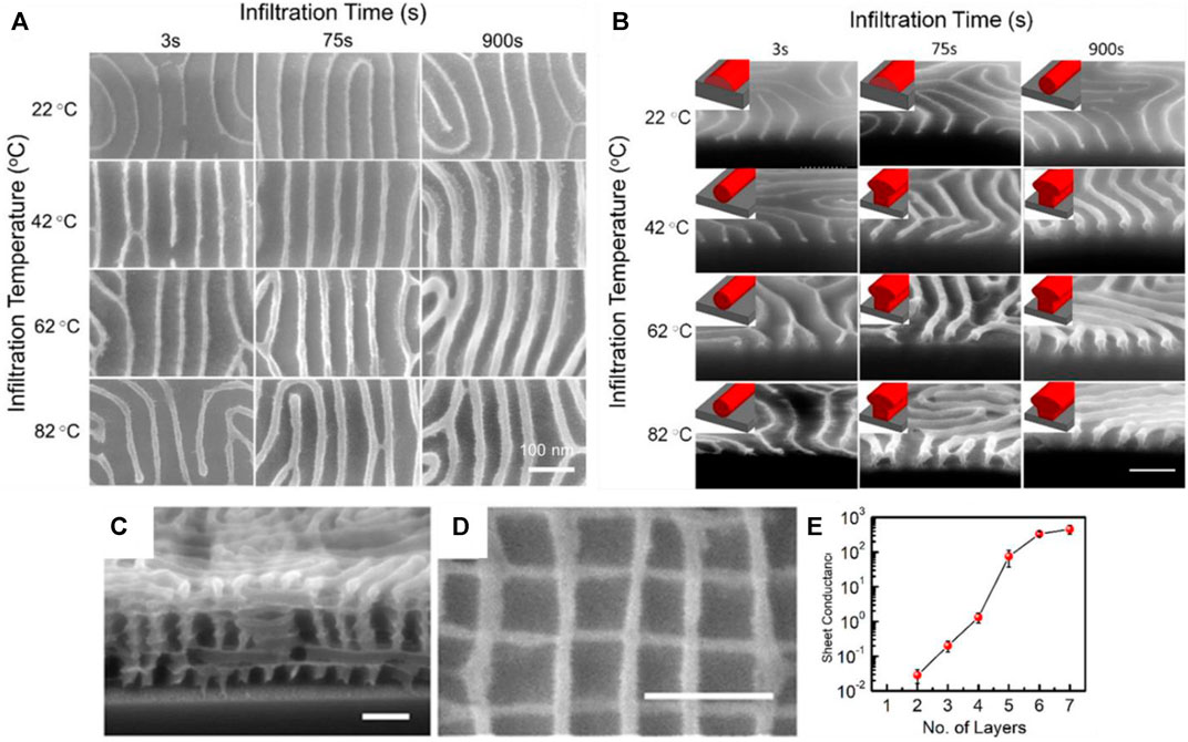
FIGURE 8. Evolution of Pt nanowire linewidth, height, and cross-sectional shape upon changing infiltration soak time and temperature (A) Top-view and (B) cross-sectional SEM images with insets depicting schematic cross-sectional shapes; High-magnification cross-sectional (C) and top-view (D) SEM micrograph images of a seven-layer Pt nanomesh; (E) Stack-layer-number-dependent electrical conductance of Pt nanoarchitectures. All scale bars denote 100 nm. Reproduced with permission from ref (Subramanian et al., 2020).
Laser-based photothermal annealing of BCP thin films can be also used to force the morphologies to shear align in the direction of the laser movement and can be combined with LPI to obtain orthogonally aligned nanowires and nanoarchitectures with reproducible material properties. For instance, Majewski and Yager et al. demonstrated laser zone annealing where energy of a focused laser beam was used to locally heat the substrate coated with the BCP using a germanium underlayer. (Majewski et al., 2015) The entire sample was rapidly annealed by sweeping the laser beam in the desired direction, and the localized temperature rise under the beam led to steep thermal gradients inducing accelerated self-assembly of the BCP film. Simultaneously, PDMS cladding sheared the BCP film in the sweep direction leading to its thermal expansion and alignment in the sweep direction (Figures 9A,B). Fabrication of multi-layered inorganic (metal, metal oxide and their combination) nanomesh structures enabled by using both VPI and LPI in the laser-zone-annealed BCP thin film templates was also demonstrated, (Majewski et al., 2015), and up to three layers of inorganic nanowire arrays were successively stacked to generate nanomesh structures with controlled pattern symmetries. The electrical resistivity of the Pt nanowires could be controlled and tuned between ∼1010–105 Ω μm−1 by changing the sintering temperature (Figure 9C) and the perfectly aligned two-layered Pt nanomesh displayed isotropic electrical properties along the longitudinal and transverse direction of an aligned square grid (Figure 9D). (Majewski et al., 2015)
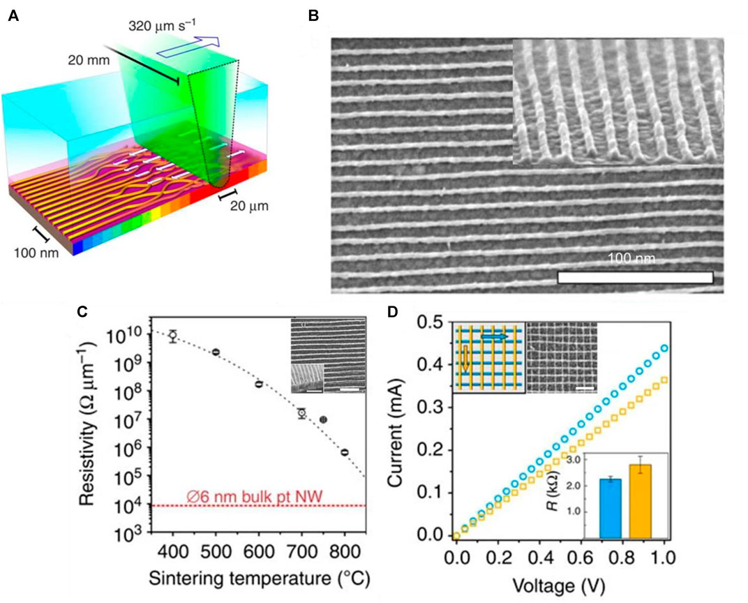
FIGURE 9. (A) Schematic representation of the laser zone annealing for shear alignment of BCP thin films; (B) SEM micrograph showing the top-view (and inset showing cross-sectional view) of Pt nanowires (soak time: 1 h, precursor: 0.02 M Na2PtCl4 in 0.5 M HCl) produced after polymer ashing; (C) Electrical resistivity (resistance per unit length of the wire) measured at room temperature as a function of sintering temperature (5 min in 5% H2 in Ar). At 800 °C, resistivity approaches bulk Pt (dashed red line) with inset SEM micrograph of single layer aligned Pt nanowires; (D) I–V characteristics of the square grid; electrical properties are nearly isotropic. Error bars represent standard deviation. for atleast8 devices. Reproduced with permission from ref (Majewski et al., 2015).
It is also possible to fabricate aligned inorganic nanostructures, by combining DSA of BCP with LPI, potentially useful for various applications. For instance, Buriak and coworkers overcome the lack of long-range order in fingerprint patterned Pt and Au nanowires structures synthesized using LPI, by using silicon-based trenches as guiding lines to align the self-assembly of PS-b-P2VP cylindrical morphology (Figures 10A,B). (Chai et al., 2007; Chai and Buriak, 2008) The conductivity of the individual wires were measured using conductive atomic force microscopy (C-AFM) equipped with a platinum-coated silicon tip. By increasing the salt concentration from 0.1 to 10 mM during the LPI process (Figure 10C), the Pt mass loading and hence the wire dimensions were increased (height from ∼7.2 to ∼11.6 nm and the width from ∼9.2 to ∼13.5 nm). As the metal loading increased, the resistance of these individual nanowires decreased from 3.0 kΩ nm−1 to ∼1.2 kΩ nm−1 (Figure 10D). (Chai et al., 2007)
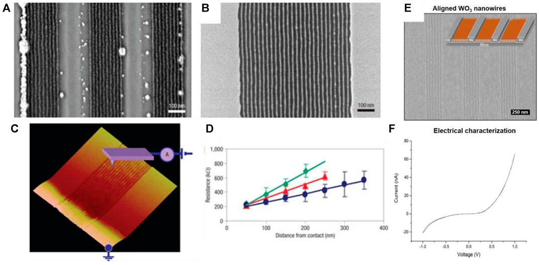
FIGURE 10. SEM images of metallic nanowires aligned in silicon trenches; (A) Au nanowires after exposure to 10 mM HAuCl4/0.9% HF (aq.) for 10 min followed by 30 s oxygen plasma ashing; (B) Pt nanostructures after performing LPI with 10 mM Na2PtCl4 in0.9% HCl (aq.) for 3 h followed by 30 s oxygen plasma and 5 s argon plasma ashing; (C) Schematic diagram showing C-AFM for probing the electrical resistance of platinum nanowires; (D) Resistance changeas distance from the contact pads for three different platinum nanowire arrays obtained by immersion into Na2PtCl4 concentrations of 0.1 mM (green), 1 mM (red) and 10 mM (blue), and their corresponding resistances were 3.0 kΩ nm−1, 1.9 kΩ nm−1 and 1.2 kΩ nm−1, respectively; (E) WO3 nanowires following metal salt inclusion and UV/O3; (F) I-V curves of contacted WO3 nanowires. Reproduced with permission from ref (Chai et al., 2007; Cummins et al., 2017).
Cummins and Morris et al. similarly fabricated aligned WO3 by utilizing graphoepitaxy of PS-b-P4VP. (Cummins et al., 2017) The Si substrate was patterned with silsesquioxane (SSQ)-based trenches by nanoimprint lithography. PS-b-P4VP thin films were self-assembled on the pre-patterned substrate which enabled aligned BCP thin film, and subsequently converted into WO3 using LPI process (Figure 10E). Electrical characterization was performed by putting Ti/Au electrodes on the aligned WO3 nanowires. The electrical characterization revealed that irrespective of the number of trenches, the measured resistivity was 10 MΩ cm (Figure 10F).
Infiltration-Modified Block Copolymer Films for Lithographic Pattern Transfer into Functional Substrates
BCP thin films have also been used as masks for pattern transfer to underlying substrates such as Si for device applications. Jeong, Kim and Lee et al., for instance, demonstrated the electrical detection of biomolecules using FET-type biosensor on a nanopatterned silicon surface fabricated by the bottom-up BCP self-assembly process. (Jeong et al., 2014) Vertical hexagonal cylinder arrays of a PS-b-PMMA thin film were used as a template for generating Si nanomesh structures with sub-20 nm features. Here, the PMMA domain of the BCP was removed using UV-acetic acid process and the remaining PS template was used as the etch mask to transfer patterns into underlying Si. The Si nanomesh structure was functionalized with biotin molecules for sensing avidin or streptavidin proteins. More importantly, a very thick layer of BCP film (∼110 nm) was required to be used as the etch mask because of its poor etch resistance of the organic PS nanostructures. Using organic BCP films may not be a feasible way for patterning high aspect ratio structures for the same reason.
Traditional photoresists are typically composed of carbon, oxygen showing poor etch resistance and thus are insufficient for fabricating high-aspect-ratio nanostructures on the underlying substrate by etching-based pattern transfer. Tseng, Darling, and Elam et al. have shown that SIS of AlOx into a patterned photoresist could significantly enhance the etch resistance, therefore facilitating etching-based, high-aspect-ratio pattern transfer onto the Si substrate, which otherwise would have required a sacrificial hard mask underlayer. (Tseng et al., 2011; TsengTseng et al., 2011; Tseng et al., 2012)
Similar to the traditional photoresists, BCP films can also be hybridized via VPI and the hybrid can be directly used as an etch mask. Specifically, improved etch resistance of self-assembled PS-b-PMMA BCP thin-film templates was demonstrated by Tseng, Elam, and Darling et al. via AlOx infiltration using the SIS process (Figure 11A). (TsengTseng et al., 2011) The AlOx-infiltrated BCP films also enabled transfer of BCP patterns into Si substrates to pattern high aspect ratio (10:1) Si nanostructures which are of interest for new type of transistor design, such as the fin-structure (Figure 11 b,c). The AlOx infiltrated BCP films also showed very good etch resistance for pattern transfer into other substrates, such as indium tin oxide (ITO) (Figure 11D), which has potential applications in photovoltaics and optoelectronics, and permalloy (Ni0.8Fe0.2) (Figure 11E) that typically requires an intermediate hard mask for pattern transfer due to a very low etch rate.
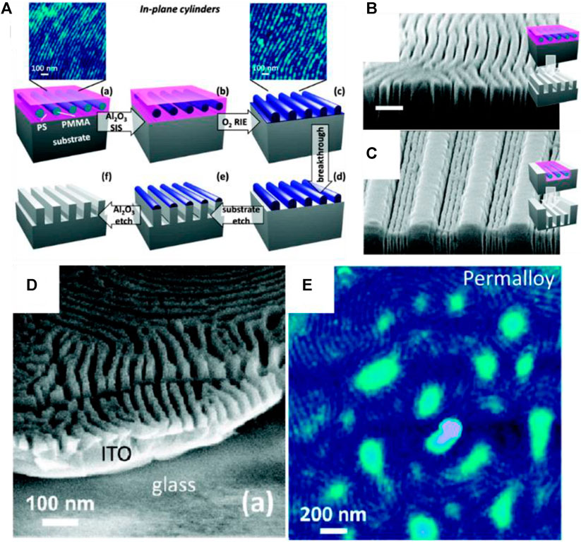
FIGURE 11. (A) Schematic for patterning underlying substrates using infiltrated hybrid BCPs with in plane cylinder morphology; Pattern transfer into underlying silicon using HBr-based plasma, with AlOx infiltrated PS-b-PMMA film as etch mask (B) from in-plane PMMA cylinders. (C) BCP film aligned using graphoepitaxy; pattern transfer using the BCP-AlOx hybrid film into (D) indium tin oxide using plasma etching; and into (E) permalloy (Ni0.8Fe0.2) using CO-based plasma etching. Reproduced with permission from ref (TsengTseng et al., 2011).
Infiltration synthesis in self-assembled BCP thin films also allows direct patterning of nanotextured surfaces on target substrates; Rahman, Liapis and Black et al. modified Si and SiO2 substrates by decorating the surface with antireflective nanocones that resulted in increased Si solar cell efficiency (Rahman et al., 2015) and improved transparency of window glass. (Rahman et al., 2014; Liapis et al., 2017) The nanocones were fabricated directly on the substrate by transferring BCP templated AlOx nanodot patterns to the underlying substrate via inductively coupled plasma reactive ion etching of Si (Figure 12B). By tuning the etching gas composition (comprising HBr:Cl2:O2 or SF6:O2) and etching time, the physical features of the nanocones (height and tapering angle) could be controlled. The Si solar cells with nanotextures showed improved photovoltaic power conversion efficiency from 8.7% (no nanotextures) to 13.1% (Rahman et al., 2015) (Figures 12C,D), and similar structures on glass windows had ultrahigh transparency (<0.2% reflectivity) applicable to solar cells. (Liapis et al., 2017) These nanocones can also be useful for fabricating more efficient separation micro/nanofluidic devices, filtration membranes, or high-performance electrodes. (Al Hossain et al., 2020) AlOx nanodots created by infiltration synthesis in self-assembled PS-b-PMMA could be also integrated into polymer solar cells for improving device power conversion efficiency by increasing the light absorption by optical scattering and charge collection by creating a protruded electrode structure. (Carpenter et al., 2017)
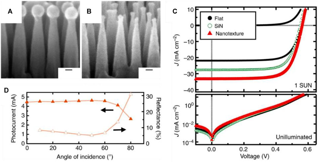
FIGURE 12. 70°-tilted SEM images of nanotextures (A) before and (B) after removal of Alox nanodots; (C) Illuminated (1 SUN) and unilluminated current–voltage (J–V) characteristics of flat silicon solar cell (black) and similar cells coated with an silicon nitride antireflection coating of 80 nm (green open circles) and a surface nanotextured using the BCP template (red); d) Angular dependence of device photocurrent (solid red triangles) and reflectance (red open triangles) when illuminated with 632-nm light. Left and right arrows refer plotted data to the appropriate horizontal axes. Reproduced with permission from ref (Rahman et al., 2015).
Conclusion
Self-assembled BCP thin films have emerged as a nontraditional material patterning platform, when combined with strategies to convert these nanomorphologies into more useful functional inorganic nanostructures for applications in nanodevices. Various post-self-assembly modification processes, including thin-film deposition and lift-off, VPI and LPI hybridization, and plasma-etching-based pattern transfer, have enabled the generation of various nanostructured semiconductors, metals and conductive polymer nanostructures for various device applications such as in opto-chemical sensors, solar cells. Given the large-area scalability, ease of processing, and the various inorganic pattern generation and conversion methods, self-assembled BCP thin films promise widening practical applications for various electrical, electronic, and optoelectronic devices in the future.
Author Contributions
AS, NT, W-IL and C-YN cowrote the manuscript.
Funding
The research was carried out at the Center for Functional Nanomaterials (CFN), Brookhaven National Laboratory (BNL), and is supported by the United States Department of Energy, Office of Basic Energy Sciences, under Contract No. DE-SC0012704.
Conflict of Interest
The authors declare that the research was conducted in the absence of any commercial or financial relationships that could be construed as a potential conflict of interest.
Publisher’s Note
All claims expressed in this article are solely those of the authors and do not necessarily represent those of their affiliated organizations, or those of the publisher, the editors, and the reviewers. Any product that may be evaluated in this article, or claim that may be made by its manufacturer, is not guaranteed or endorsed by the publisher.
References
Aizawa, M., and Buriak, J. M. (2006). Nanoscale Patterning of Two Metals on Silicon Surfaces Using an ABC Triblock Copolymer Template. J. Am. Chem. Soc. 128 (17), 5877–5886. doi:10.1021/ja060366x
Al Hossain, A., Yang, M., Checco, A., Doerk, G., and Colosqui, C. E. (2020). Large-area Nanostructured Surfaces with Tunable Zeta Potentials. Appl. Mater. Today 19, 100553. doi:10.1016/j.apmt.2019.100553
Amir Tavakkoli, K. G., Nicaise, S. M., Gadelrab, K. R., Alexander-Katz, A., Ross, C. A., and Berggren, K. K. (2016). Multilayer Block Copolymer Meshes by Orthogonal Self-Assembly. Nat. Commun. 7, 1. doi:10.1038/ncomms105181
Bamford, J. T., Smith, R. A., Leng, C. Z., Gutekunst, W. R., and Losego, M. D. (2021). Measuring the Glass Transition Temperature of Vapor-Phase-Infiltrated AlOx-PS-R-PHEMA Organic-Inorganic Hybrid Thin-Film Materials. Macromolecules 54 (14), 6790–6798. doi:10.1021/acs.macromol.1c00691
Barrera, G., Celegato, F., Coïsson, M., Manzin, A., Ferrarese Lupi, F., Seguini, G., et al. (2017). Magnetization Switching in High-Density Magnetic Nanodots by a fine-tune Sputtering Process on a Large-Area Diblock Copolymer Mask. Nanoscale 9 (43), 16981–16992. doi:10.1039/c7nr04295g
Barry, E., Mane, A. U., Libera, J. A., Elam, J. W., and Darling, S. B. (2017). Advanced Oil Sorbents Using Sequential Infiltration Synthesis. J. Mater. Chem. A. 5 (6), 2929–2935. doi:10.1039/c6ta09014a
Barun, K. (2019). Barick, Assaf Simon, Inbal Weisbord, Neta Shomrat, and Tamar Segal-Peretz. J. Colloid Interf. Sci. 557, 537. doi:10.1016/j.jcis.2019.09.044
Berman, D., and Shevchenko, E. (2020). Design of Functional Composite and All-Inorganic Nanostructured Materials via Infiltration of Polymer Templates with Inorganic Precursors. J. Mater. Chem. C 8 (31), 10604–10627. doi:10.1039/d0tc00483a
Black, C. T., Ruiz, R., Breyta, G., Cheng, J. Y., Colburn, M. E., Guarini, K. W., et al. (2007). Polymer Self Assembly in Semiconductor Microelectronics. IBM J. Res. Dev. 51 (5), 605–633. doi:10.1147/rd.515.0605
Campbell, I. P., Lau, G. J., Feaver, J. L., and Stoykovich, M. P. (2012). Network Connectivity and Long-Range Continuity of Lamellar Morphologies in Block Copolymer Thin Films. Macromolecules 45 (3), 1587–1594. doi:10.1021/ma2025336
Carpenter, C. L., Nicaise, S., Theofanis, P. L., Shykind, D., Berggren, K. K., Delaney, K. T., et al. (2017). Orientational Preference in Multilayer Block Copolymer Nanomeshes with Respect to Layer-To-Layer Commensurability. Macromolecules 50 (20), 8258–8266. doi:10.1021/acs.macromol.7b01290
Chai, J., and Buriak, J. M. (2008). Using Cylindrical Domains of Block Copolymers to Self-Assemble and Align Metallic Nanowires. ACS Nano 2 (3), 489–501. doi:10.1021/nn700341s
Chai, J., Wang, D., Fan, X., and Buriak, J. M. (2007). Assembly of Aligned Linear Metallic Patterns on Silicon. Nat. Nanotech 2 (8), 500–506. doi:10.1038/nnano.2007.227
Cheng, J. Y., Sanders, D. P., Truong, H. D., Harrer, S., Alexander, F., Holmes, S., et al. (2010). Simple and Versatile Methods to Integrate Directed Self-Assembly with Optical Lithography Using a Polarity-Switched Photoresist. ACS Nano 4 (8), 4815. doi:10.1021/nn100686v
Cummins, C., Bell, A. P., and Morris, M. A. (2017). Nanomaterials (Basel) 7 (10), 1. doi:10.3390/nano7100304
Cummins, C., Borah, D., Rasappa, S., Chaudhari, A., Ghoshal, T., O’Driscoll, B. M. D., et al. (2013). Self-assembly of Polystyrene-Block-Poly(4-Vinylpyridine) Block Copolymer on Molecularly Functionalized Silicon Substrates: Fabrication of Inorganic Nanostructured Etchmask for Lithographic Use. J. Mater. Chem. C 1 (47), 7841. doi:10.1039/c3tc31498g
Cummins, C., Gangnaik, A., Kelly, R. A., Borah, D., O'Connell, J., Petkov, N., et al. (2015). Aligned Silicon Nanofins via the Directed Self-Assembly of PS-B-P4vp Block Copolymer and Metal Oxide Enhanced Pattern Transfer. Nanoscale 7 (15), 6712–6721. doi:10.1039/c4nr07679f
Cummins, C., Ghoshal, T., Holmes, J. D., and Morris, M. A. (2016). Strategies for Inorganic Incorporation Using Neat Block Copolymer Thin Films for Etch Mask Function and Nanotechnological Application. Adv. Mater. 28 (27), 5586–5618. doi:10.1002/adma.201503432
Diederichsen, K. M., Brow, R. R., and Stoykovich, M. P. (2015). Percolating Transport and the Conductive Scaling Relationship in Lamellar Block Copolymers under Confinement. ACS Nano 9 (3), 2465–2476. doi:10.1021/acsnano.5b01321
Doerk, G. S., Li, R., Fukuto, M., and Yager, K. G. (2020). Wet Brush Homopolymers as "Smart Solvents" for Rapid, Large Period Block Copolymer Thin Film Self-Assembly. Macromolecules 53 (3), 1098–1113. doi:10.1021/acs.macromol.9b02296
Doerk, G. S., and Yager, K. G. (2017). Rapid Ordering in "Wet Brush" Block Copolymer/Homopolymer Ternary Blends. ACS Nano 11 (12), 12326–12336. doi:10.1021/acsnano.7b06154
Dusoe, K. J., Ye, X., Kisslinger, K., Stein, A., Lee, S.-W., and Nam, C.-Y. (2017). Ultrahigh Elastic Strain Energy Storage in Metal-Oxide-Infiltrated Patterned Hybrid Polymer Nanocomposites. Nano Lett. 17 (12), 7416–7423. doi:10.1021/acs.nanolett.7b03238
Evangelio, L., Fernández-Regúlez, M., Fraxedas, J., Müller, M., and Pérez-Murano, F. (2019). Role of Penetrability into a Brush-Coated Surface in Directed Self-Assembly of Block Copolymers. ACS Appl. Mater. Inter. 11 (3), 3571–3581. doi:10.1021/acsami.8b19062
Frascaroli, J., Brivio, S., Ferrarese Lupi, F., Seguini, G., Boarino, L., Perego, M., et al. (2015). Resistive Switching in High-Density Nanodevices Fabricated by Block Copolymer Self-Assembly. ACS Nano 9 (3), 2518–2529. doi:10.1021/nn505131b
Ghoshal, T., Fleming, P. G., Holmes, J. D., and Morris, M. A. (2012). The Stability of “Ce2O3” Nanodots in Ambient Conditions: a Study Using Block Copolymer Templated Structures. J. Mater. Chem. 22 (43). doi:10.1039/c2jm35073d
Ghoshal, T., Chaudhari, A., Cummins, C., Shaw, M. T., Holmes, J. D., and Morris, M. A. (2016). Morphological Evolution of Lamellar Forming Polystyrene-Block-Poly(4-Vinylpyridine) Copolymers under Solvent Annealing. Soft Matter 12 (24), 5429–5437. doi:10.1039/c6sm00815a
Gottlieb, S., Fernández-Regúlez, M., Lorenzoni, M., Evangelio, L., and Perez-Murano, F. (2020). Grain-Boundary-Induced Alignment of Block Copolymer Thin Films. Nanomaterials 10 (1). doi:10.3390/nano10010103
Gregorczyk, K. E., Pickup, D. F., Sanz, M. G., Irakulis, I. A., Rogero, C., and Knez, M. (2015). Tuning the Tensile Strength of Cellulose through Vapor-phase Metalation. Chem. Mater. 27 (1), 181–188. doi:10.1021/cm503724c
Greil, S., Rahman, A., Liu, M., and Black, C. T. (2017). Gas Transport Selectivity of Ultrathin, Nanoporous, Inorganic Membranes Made from Block Copolymer Templates. Chem. Mater. 29 (21), 9572–9578. doi:10.1021/acs.chemmater.7b04174
Han, E., Kang, H., Liu, C.-C., Nealey, P. F., and Gopalan, P. (2010). Graphoepitaxial Assembly of Symmetric Block Copolymers on Weakly Preferential Substrates. Adv. Mater. 22 (38), 4325–4329. doi:10.1002/adma.201001669
He, C., and Stoykovich, M. P. (2014). Profile Control in Block Copolymer Nanostructures Using Bilayer Thin Films for Enhanced Pattern Transfer Processes. Adv. Funct. Mater. 24, 7078–7084. doi:10.1002/adfm.201401810
Hu, H., Gopinadhan, M., and Osuji, C. O. (2014). Directed Self-Assembly of Block Copolymers: a Tutorial Review of Strategies for Enabling Nanotechnology with Soft Matter. Soft Matter 10 (22), 3867. doi:10.1039/c3sm52607k
Jeong, C. K., Jin, H. M., Ahn, J.-H., Park, T. J., Yoo, H. G., Koo, M., et al. (2014). Electrical Biomolecule Detection Using Nanopatterned Silicon via Block Copolymer Lithography. Small 10 (2), 337–343. doi:10.1002/smll.201301202
Jung, Y. S., Jung, W., Tuller, H. L., and Ross, C. A. (2008). Nanowire Conductive Polymer Gas Sensor Patterned Using Self-Assembled Block Copolymer Lithography. Nano Lett. 8 (11), 3776–3780. doi:10.1021/nl802099k
Kamcev, J., Germack, D. S., Nykypanchuk, D., Grubbs, R. B., Nam, C.-Y., and Black, C. T. (2013). Chemically Enhancing Block Copolymers for Block-Selective Synthesis of Self-Assembled Metal Oxide Nanostructures. ACS Nano 7 (1), 339–346. doi:10.1021/nn304122b
Kim, H.-C., Park, S.-M., and Hinsberg, W. D. (2010). Block Copolymer Based Nanostructures: Materials, Processes, and Applications to Electronics. Chem. Rev. 110 (1), 146–177. doi:10.1021/cr900159v
Laura, E., Marta, F.-R., Xavier, B., Matteo, L., Jordi, F., and Francesc, P.-M. (2015). Creation of Guiding Patterns for Directed Self-Assembly of Block Copolymers by Resistless Direct E-Beam Exposure. J. Micro/Nanolithography, MEMS, MOEMS 14 (3), 1.
Lee, S., Lee, W., Jung, H.-T., and Ross, C. A. (2021). Selective Deposition of Copper on Self-Assembled Block Copolymer Surfaces via Physical Vapor Deposition. ACS Appl. Mater. Interfaces 13 (44), 52931–52937.
Lee, S.-M., Pippel, E., Gösele, U., Dresbach, C., Qin, Y., Chandran, C. V., et al. (2009). Greatly Increased Toughness of Infiltrated Spider Silk. Science 324 (5926), 488–492. doi:10.1126/science.1168162
Lee, S.-M., Pippel, E., Moutanabbir, O., Gunkel, I., Thurn-Albrecht, T., and Knez, M. (2010). Improved Mechanical Stability of Dried Collagen Membrane after Metal Infiltration. ACS Appl. Mater. Inter. 2 (8), 2436–2441. doi:10.1021/am100438b
Leng, C. Z., and Losego, M. D. (2017). Vapor Phase Infiltration (VPI) for Transforming Polymers into Organic-Inorganic Hybrid Materials: a Critical Review of Current Progress and Future Challenges. Mater. Horiz. 4 (5), 747–771. doi:10.1039/c7mh00196g
Liapis, A. C., Rahman, A., and Black, C. T. (2017). Self-assembled Nanotextures Impart Broadband Transparency to Glass Windows and Solar Cell Encapsulants. Appl. Phys. Lett. 111 (18), 183901. doi:10.1063/1.5000965
Lin, C.-H., Polisetty, S., O’Brien, L., Baruth, A., Hillmyer, M. A., Leighton, C., et al. (2015). Size-Tuned ZnO Nanocrucible Arrays for Magnetic Nanodot Synthesis via Atomic Layer Deposition-Assisted Block Polymer Lithography. ACS Nano 9 (2), 1379–1387. doi:10.1021/nn505731n
Luka, G., Krajewski, T. A., Witkowski, B. S., Wisz, G., Virt, I. S., Guziewicz, E., et al. (2011). Aluminum-doped Zinc Oxide Films Grown by Atomic Layer Deposition for Transparent Electrode Applications. J. Mater. Sci. Mater. Electron. 22 (12), 1810–1815. doi:10.1007/s10854-011-0367-0
Majewski, P. W., Rahman, A., Black, C. T., and Yager, K. G. (2015). Arbitrary Lattice Symmetries via Block Copolymer Nanomeshes. Nat. Commun. 6, 1. doi:10.1038/ncomms8448
McGuinness, E. K., Leng, C. Z., and Losego, M. D. (2020). Increased Chemical Stability of Vapor-phase Infiltrated AlOx-Poly(methyl Methacrylate) Hybrid Materials. ACS Appl. Polym. Mater. 2 (3), 1335–1344. doi:10.1021/acsapm.9b01207
Nam, C.-Y., Stein, A., and Kim, K. (2015). Direct Fabrication of High Aspect-Ratio Metal Oxide Nanopatterns via Sequential Infiltration Synthesis in Lithographically Defined SU-8 Templates. J. Vac. Sci. Technol. B: 33 (6), 1. doi:10.1116/1.4929508
Nam, C. Y., Stein, A., Kim, K., and Charles, T. (2015). Electrical and Structural Properties of ZnO Synthesized via Infiltration of Lithographically Defined Polymer Templates. Black, Appl. Phys. Lett. 107 (20), 1. doi:10.1063/1.4935793
Nam, C. Y., and Stein, A. (2017). Photodetectors: Extreme Carrier Depletion and Superlinear Photoconductivity in Ultrathin Parallel-Aligned ZnO Nanowire Array Photodetectors Fabricated by Infiltration Synthesis (Advanced Optical Materials 24/2017). Adv. Opt. Mater. 5 (24), 1. doi:10.1002/adom.201770119
Ocola, L. E., Gosztola, D. J., Yanguas-Gil, A., Suh, H.-S., and Connolly, A. (2016). Quantum Sensing and Nano Electronics and Photonics XIII. San Francisco, California, United States: SPIE - International Society for Optics and Photonics.
Oria, L., Ruiz de Luzuriaga, A., Alduncin, J. A., and Perez-Murano, F. (2013). Polystyrene as a brush Layer for Directed Self-Assembly of Block Co-polymers. Microelectronic Eng. 110, 234–240. doi:10.1016/j.mee.2012.12.006
Peng, Q., TsengTseng, Y.-C., Darling, S. B., and Elam, J. W. (2011). A Route to Nanoscopic Materials via Sequential Infiltration Synthesis on Block Copolymer Templates. ACS Nano 5 (6), 4600–4606. doi:10.1021/nn2003234
Peng, Q., TsengTseng, Y.-C., Darling, S. B., and Elam, J. W. (2010). Nanoscopic Patterned Materials with Tunable Dimensions via Atomic Layer Deposition on Block Copolymers. Adv. Mater. 22 (45), 5129–5133. doi:10.1002/adma.201002465
Pinto-Gomez, C., Perez-Murano, F., Bausells, J., Villanueva, L. G., and Fernandez-Regulez, M. (2020). Directed Self-Assembly of Block Copolymers for the Fabrication of Functional Devices. Polymers (Basel) 12 (10). doi:10.3390/polym12102432
Pleshek, D., Tran, J., Li, Y., Shirani, A., Shevchenko, E. V., and Berman, D. (2021). Swelling-Assisted Sequential Infiltration Synthesis of Nanoporous ZnO Films with Highly Accessible Pores and Their Sensing Potential for Ethanol. ACS Appl. Mater. Inter. 13 (30), 35941–35948. doi:10.1021/acsami.1c08225
Rahman, A., Ashraf, A., Xin, H., Tong, X., Sutter, P., Eisaman, M. D., et al. (2015). Sub-50-nm Self-Assembled Nanotextures for Enhanced Broadband Antireflection in Silicon Solar Cells. Nat. Commun. 6, 1. doi:10.1038/ncomms6963
Rahman, A., Majewski, P. W., Doerk, G., Black, C. T., and Yager, K. G. (2016). Non-native Three-Dimensional Block Copolymer Morphologies. Nat. Commun. 7, 1. doi:10.1038/ncomms13988
Rahman, A., Liu, M., and Black, C. T. (2014). Block Copolymer Self Assembly for Design and Vapor-phase Synthesis of Nanostructured Antireflective Surfaces. J. Vacuum Sci. Tech. B, Nanotechnology Microelectronics: Mater. Process. Meas. Phenomena 32 (6), 06FE02. doi:10.1116/1.4896335
Segalman, R. A. (2005). Patterning with Block Copolymer Thin Films. Mater. Sci. Eng. R. Rep. 48 (6), 191. doi:10.1016/j.mser.2004.12.003
Shin, D. O., Jeong, J.-R., Han, T. H., Koo, C. M., Park, H.-J., Lim, Y. T., et al. (2010). A Plasmonic Biosensor Array by Block Copolymer Lithography. J. Mater. Chem. 20 (34), 7241. doi:10.1039/c0jm01319f
Shin, D. O., Mun, J. H., Hwang, G.-T., Yoon, J. M., Kim, J. Y., Yun, J. M., et al. (2013). Multicomponent Nanopatterns by Directed Block Copolymer Self-Assembly. ACS Nano 7 (10), 8899–8907. doi:10.1021/nn403379k
Subramanian, A., Doerk, G., Kisslinger, K., Yi, D. H., Grubbs, R. B., and Nam, C.-Y. (2019). Three-dimensional Electroactive ZnO Nanomesh Directly Derived from Hierarchically Self-Assembled Block Copolymer Thin Films. Nanoscale 11, 9533–9546. doi:10.1039/c9nr00206e
Subramanian, A., Tiwale, N., Doerk, G., Kisslinger, K., and Nam, C.-Y. (2020). Enhanced Hybridization and Nanopatterning via Heated Liquid-phase Infiltration into Self-Assembled Block Copolymer Thin Films. ACS Appl. Mater. Inter. 12 (1), 1444–1453. doi:10.1021/acsami.9b16148
Subramanian, A., Tiwale, N., and Nam, C.-Y. (2018). Review of Recent Advances in Applications of Vapor-phase Material Infiltration Based on Atomic Layer Deposition. JOM 71 (1), 185–196. doi:10.1007/s11837-018-3141-4
Tseng, Y.-C., and Darling, S. B. (2010). Block Copolymer Nanostructures for Technology. Polymers 2, 470–489. doi:10.3390/polym2040470
Tseng, Y.-C., Mane, A. U., Elam, J. W., and Darling, S. B. (2012). Enhanced Lithographic Imaging Layer Meets Semiconductor Manufacturing Specification a Decade Early. Adv. Mater. 24 (19), 2608–2613. doi:10.1002/adma.201104871
Tseng, Y.-C., Peng, Q., Ocola, L. E., Czaplewski, D. A., Elam, J. W., and Darling, S. B. (2011). Enhanced Polymeric Lithography Resists via Sequential Infiltration Synthesis. J. Mater. Chem. 21 (32), 11722. doi:10.1039/c1jm12461g
TsengTseng, Y.-C., Peng, Q., Ocola, L. E., Elam, J. W., and Darling, S. B. (2011). Enhanced Block Copolymer Lithography Using Sequential Infiltration Synthesis. J. Phys. Chem. C 115 (36), 17725–17729. doi:10.1021/jp205532e
Varghese, J., Ghoshal, T., Deepak, N., O’Regan, C., Whatmore, R. W., Morris, M. A., et al. (2013). Fabrication of Arrays of Lead Zirconate Titanate (PZT) Nanodots via Block Copolymer Self-Assembly. Chem. Mater. 25 (8), 1458–1463. doi:10.1021/cm303759r
Waldman, R. Z., Mandia, D. J., Yanguas-Gil, A., Martinson, A. B. F., Elam, J. W., and Darling, S. B. (2019). The Chemical Physics of Sequential Infiltration Synthesis—A Thermodynamic and Kinetic Perspective. J. Chem. Phys. 151 (19), 1. doi:10.1063/1.5128108
Waldman, R. Z., Jeon, N., Mandia, D. J., Heinonen, O., Darling, S. B., and Martinson, A. B. F. (2019). Sequential Infiltration Synthesis of Electronic Materials: Group 13 Oxides via Metal Alkyl Precursors. Chem. Mater. 31 (14), 5274–5285. doi:10.1021/acs.chemmater.9b01714
Xiao, S., Yang, X., Edwards, E. W., La, Y.-H., and Nealey, P. F. (2005). Graphoepitaxy of cylinder-forming Block Copolymers for Use as Templates to Pattern Magnetic Metal Dot Arrays. Nanotechnology 16 (7), S324–S329. doi:10.1088/0957-4484/16/7/003
Yi, D. H., Nam, C.-Y., Doerk, G., Black, C. T., and Grubbs, R. B. (2019). Infiltration Synthesis of Diverse Metal Oxide Nanostructures from Epoxidized Diene-Styrene Block Copolymer Templates. ACS Appl. Polym. Mater. 1 (4), 672–683. doi:10.1021/acsapm.8b00138
You, B. K., Park, W. I., Kim, J. M., Park, K.-I., Seo, H. K., Lee, J. Y., et al. (2014). Reliable Control of Filament Formation in Resistive Memories by Self-Assembled Nanoinsulators Derived from a Block Copolymer. ACS Nano 8 (9), 9492–9502. doi:10.1021/nn503713f
Yu, Y., Li, Z., Wang, Y., Gong, S., and Wang, X. (2015). Sequential Infiltration Synthesis of Doped Polymer Films with Tunable Electrical Properties for Efficient Triboelectric Nanogenerator Development. Adv. Mater. 27 (33), 4938–4944. doi:10.1002/adma.201502546
Yu, Y., and Wang, X. (2016). Chemical Modification of Polymer Surfaces for Advanced Triboelectric Nanogenerator Development. Extreme Mech. Lett. 9, 514–530. doi:10.1016/j.eml.2016.02.019
Keywords: self-assembled block copolymer, vapor-phase infiltration, liquid-phase infiltration, sequential infiltration synthesis, nanodevice applications
Citation: Subramanian A, Tiwale N, Lee W-I and Nam C-Y (2021) Templating Functional Materials Using Self-Assembled Block Copolymer Thin-Film for Nanodevices. Front. Nanotechnol. 3:766690. doi: 10.3389/fnano.2021.766690
Received: 29 August 2021; Accepted: 15 November 2021;
Published: 06 December 2021.
Edited by:
Cian Cummins, Université de Bordeaux, FranceReviewed by:
Tsukuru Minamiki, National Institute of Advanced Industrial Science and Technology (AIST), JapanMichele Perego, National Research Council (CNR), Italy
Copyright © 2021 Subramanian, Tiwale, Lee and Nam. This is an open-access article distributed under the terms of the Creative Commons Attribution License (CC BY). The use, distribution or reproduction in other forums is permitted, provided the original author(s) and the copyright owner(s) are credited and that the original publication in this journal is cited, in accordance with accepted academic practice. No use, distribution or reproduction is permitted which does not comply with these terms.
*Correspondence: Chang-Yong Nam, cynam@bnl.gov