
 E-mail Alert
 RSS
RSS
Femtosecond laser printing of vanadium dioxide based optical meta-structures with tunable spectra engineering
-
摘要:
具有动态调控能力的微纳光学器件是近年来微纳光子学领域的研究热点,二氧化钒(VO2)作为一种常见的功能性可调谐材料,其相变前后晶态的转变导致材料本身电磁参数的变化,可用于实现对光谱的动态调控。本文利用VO2的相变特性和光敏树脂单体的光聚合特性,通过在甲基丙烯酸酯单体中掺入VO2纳米晶,制备出了有效折射率可变的光敏型聚合物纳米复合材料。在此基础上,结合飞秒激光加工技术,开发出了具有相变调控特性的高精度二维、三维微纳光学结构的一次加工成型技术。测试结果表明,该方法所研制出的微纳光学结构,在外界温度达到相变临界温度时,结构中VO2纳米晶发生热致相变,导致结构整体的有效折射率发生变化,实现了对短波段光谱的动态调控。
Abstract:Over the past few years, the field of micro-/nano- photonics has witnessed a surge in research focused on developing innovative optical devices that offer dynamic spectra engineering. Among the materials showing promise in this area, vanadium dioxide (VO2) can actively manipulate its refractive index via a phase transition process, enabling the dynamic manipulation of spectra. In this work, a photosensitive polymer nanocomposite with tunable effective refractive index is prepared by incorporating VO2 nanocrystals into methacrylate monomers, which takes advantages of the phase change characteristics of VO2 and the photopolymerization properties of the monomer. In addition, with the aid of the state-of-the-art femtosecond laser processing technology, highly precise two-dimensional and three-dimensional micro-/nano- optical structures embedded with the phase change capabilities outlined by VO2 are achieved. Fascinatingly, the spectra measurements via Fourier transform infrared spectrometer reveal that when subjected to the critical phase transition temperatures, the printed micro-/nano- structures will undergo a thermally induced phase transition of the VO2 nanocrystals embedded within them. Consequently, there is a discernible alteration in the effective refractive index of the optically functionalized structure, inspiring the dynamic manipulation of the short-band spectra.
-
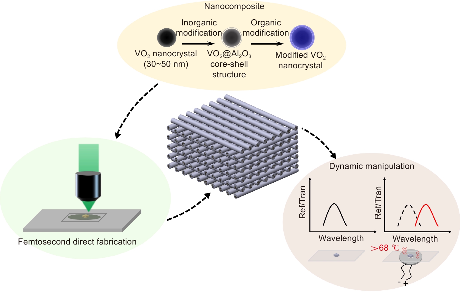
Overview: Optically functionalized meta-structures exhibit salient advantages in controlling and manipulating light-matter interactions at the micro-/nano- scale. These structures could enable a wide range of processes such as spectral engineering, phase manipulation, polarization control, filtering, modulation, optical angular momentum generation, and polarization conversion. The spectral properties of these artificial meta-structures emerge from optical resonances, which strongly relies on the size, shape, and arrangement of the metallic or dielectric meta-structures. By tailoring these parameters, it is possible to efficiently manipulate the spectra and achieve tunable spectra, especially in the near-infrared and visible range. Integrating or embedding materials or structures with tunable optical properties could be a better approach to overcome the limitation of being stuck in a fixed morphological nanostructure. As a Mott transition material, vanadium dioxide (VO2) can directly change its refractive index due to the insulating-metallic transition (IMT) at ~68 °C, which has been proved by applying temperature, electrical fields, or light triggers in the visible, infrared, and other spectral regions. By utilizing the meta-structure of vanadium dioxide, the regulation of the effective refractive index of micro-/nano- optical devices can be realized. However, the traditional electron beam lithography and focused ion beam machining are more suitable for the fabrication of 2D meta-structures, which greatly limits the device design and the spectra engineering. Compared with these processing technologies, femtosecond laser direct writing technology that utilizes focused high-intensity photon beam for processing and has the advantages such as freeform fabrication, non-conductive substrate and non-contact, is expected to meet the requirements of micro-/nano- fabrication of the VO2-based meta-structures.
In this paper, we demonstrate a feasible approach for fabricating meta-structures with flexibly manipulated effective refractive indices by incorporating VO2 nanoparticles in a matrix of acrylate resin. This approach involves tailoring the phase transition of VO2-based photosensitized nanocomposites. Through the implementation of this effective-refractive-index tailorable photosensitized nanocomposite, the direct printing of meta-structures can be achieved in a single attempt without the post-heat treatment. Therefore, it avoids the undesired structural shrinking and poor adhesion between the sample and the substrate that may occur in the traditional VO2 deposition methods like atomic layered deposition. By cross-linking polymerization reaction of the photosensitized nanocomposites, the VO2 nanocrystals are embedded into the potopolymerized structures. As a result, the optical response of the as-fabricated meat-structures could be dynamically tunable through the thermotropic phase transition of the VO2 nanocrystals in the nanocomposites. In addition, the broadband amplitude modulation of ~33% is observed in the three-dimensional hierarchical meta-structures. This strategy holds immense promise for future versatile utilization of the nanocrystal-based photosensitive nanocomposites to achieve numerous functionalities in meta-structures via femtosecond laser printing technique.
-

-
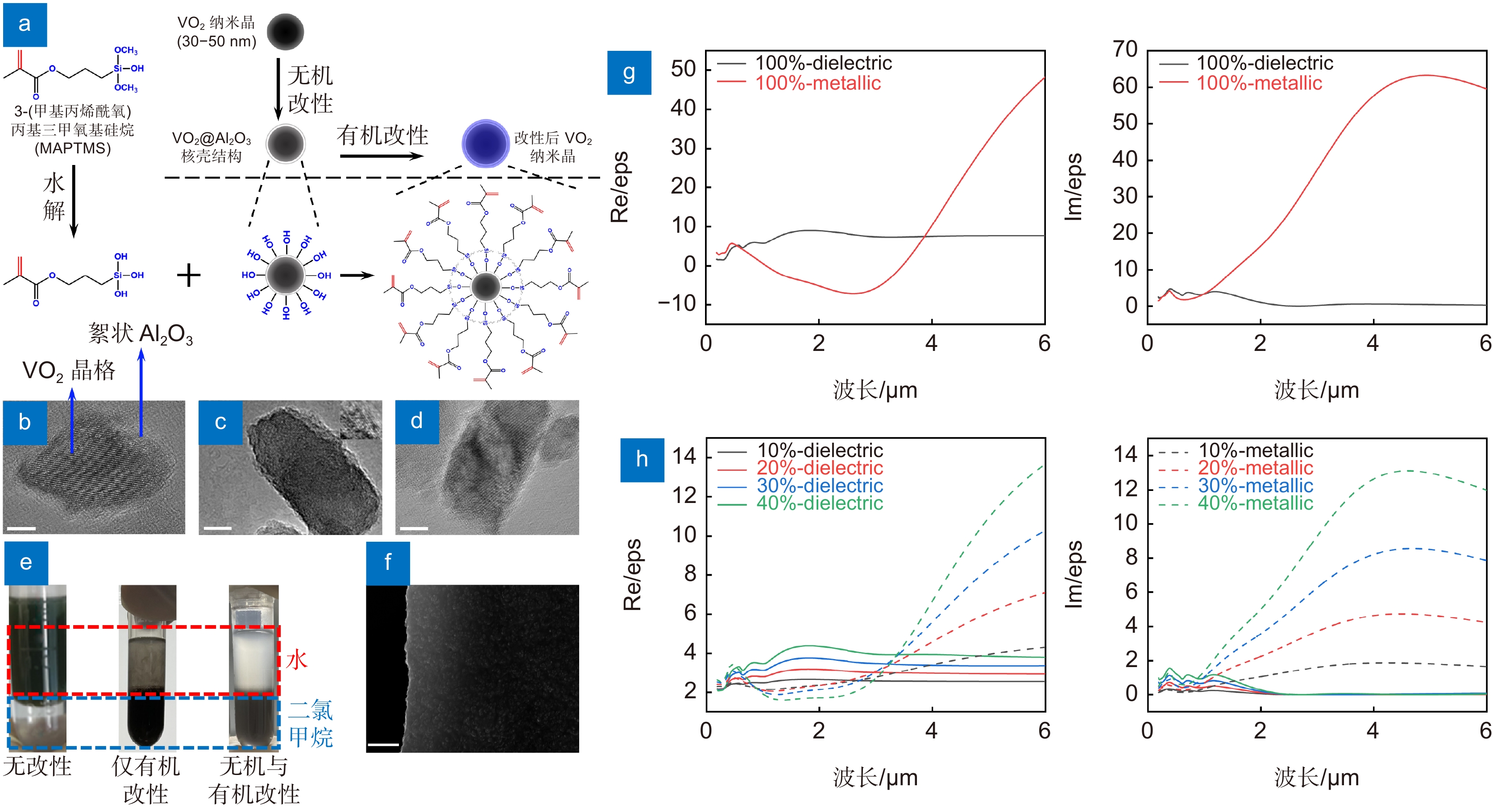
图 1 (a) VO2纳米晶颗粒无机改性与有机改性的原理、步骤示意图;(b-d) 使用三种不同无机物进行无机改性的单个VO2纳米晶颗粒的透射电子显微镜(TEM) 图片,(b)使用三氧化二铝改性,(c)使用二氧化钛改性,(d)使用二氧化硅改性,其中(b)图中VO2晶格周围存在Al2O3的无定形絮状物,标尺均为5 nm;(e) VO2纳米晶改性前后在水、二氯甲烷溶液中的分散特性对比,其中左图为未进行表面改性VO2纳米晶颗粒的分散特性,中间图为有机改性后的分散特性,右图为无机与有机改性后的分散特性;(f) 20 wt% VO2掺杂浓度的光敏型复合材料SEM图,标尺为1 μm;(g) 测试的纯VO2@Al2O3相变前后的介电常数曲线,其中左图为介电常数实部数据,右图为介电常数虚部数据,dielectric为相变前介质态,metallic为相变后类金属态;(h) 计算的10 wt%、20 wt%、30 wt%、40 wt%的VO2纳米晶光敏型复合材料升温相变前后的介电常数曲线,其中左图为介电常数实部数据,右图为介电常数虚部数据,dielectric实线为升温相变前介质态,metallic虚线为升温相变后类金属态
Figure 1. (a) Schematic diagram of the principles and steps of inorganic modification and organic modification of VO2 nanocrystal particles; (b-d) A single transmission electron microscope (TEM) picture of VO2 nanocrystalline particles, (b) modified with aluminum oxide, (c) modified with titanium dioxide, (d) modified with silicon dioxide, and there is Al2O3 appearing as amorphous flocculent around the VO2 lattice in (b). The scales are all 5 nm; (e) The comparison of dispersion characteristics of VO2 nanocrystals before and after modification in water and dichloromethane solutions, where the left picture is without surface modification, the middle picture shows the dispersion properties after organic modification, and the right picture shows the dispersion properties after inorganic modification and organic modification; (f) SEM image of the photosensitive composite material with 20 wt% VO2. The scale is 1 μm; (g) Calculated refractive index curves of 10 wt%, 20 wt%, 30 wt%, 40 wt% VO2 nanocrystalline photosensitive composite materials before and after the phase transition with the rise of the temperature, where the left picture shows the data of the real part of the refractive index, and the picture on the right shows the data of the imaginary part of the refractive index. The solid line of dielectric represents the medium state before the phase transition with the rise of the temperature, and the metallic dotted line is the metalloid state after the phase transition with the rise of the temperature
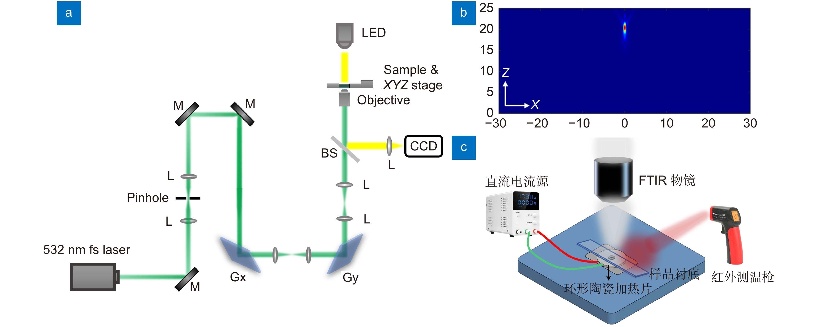
图 2 (a)飞秒激光直写加工系统光路示意图,其中M为反射镜,L为透镜,pinhole为滤波小孔,Gx与Gy为振镜系统,BS为分光棱镜,objective为物镜;(b)激光聚焦光斑的XOZ面光场分布;(c)光学器件光谱测试装置示意图,使用了环形陶瓷加热片连接直流电源对超构结构进行加热,使用红外测温枪表征超构结构的温度
Figure 2. (a) Schematic diagram of the optical path of the femtosecond laser direct writing fabrication system. Among them, M is the mirror, L is the lens, Pinhole is the filter hole, Gx and Gy are the galvanometer system, BS is the beam splitter, and Objective is the objective lens; (b) XOZ surface optical field distribution of the laser focus spot; (c) Schematic diagram of the photonic device spectrum test device, which uses a ring-shaped ceramic heating plate connected to a DC power supply to heat the photonic device and uses an infrared temperature gun to test the temperature of photonic devices
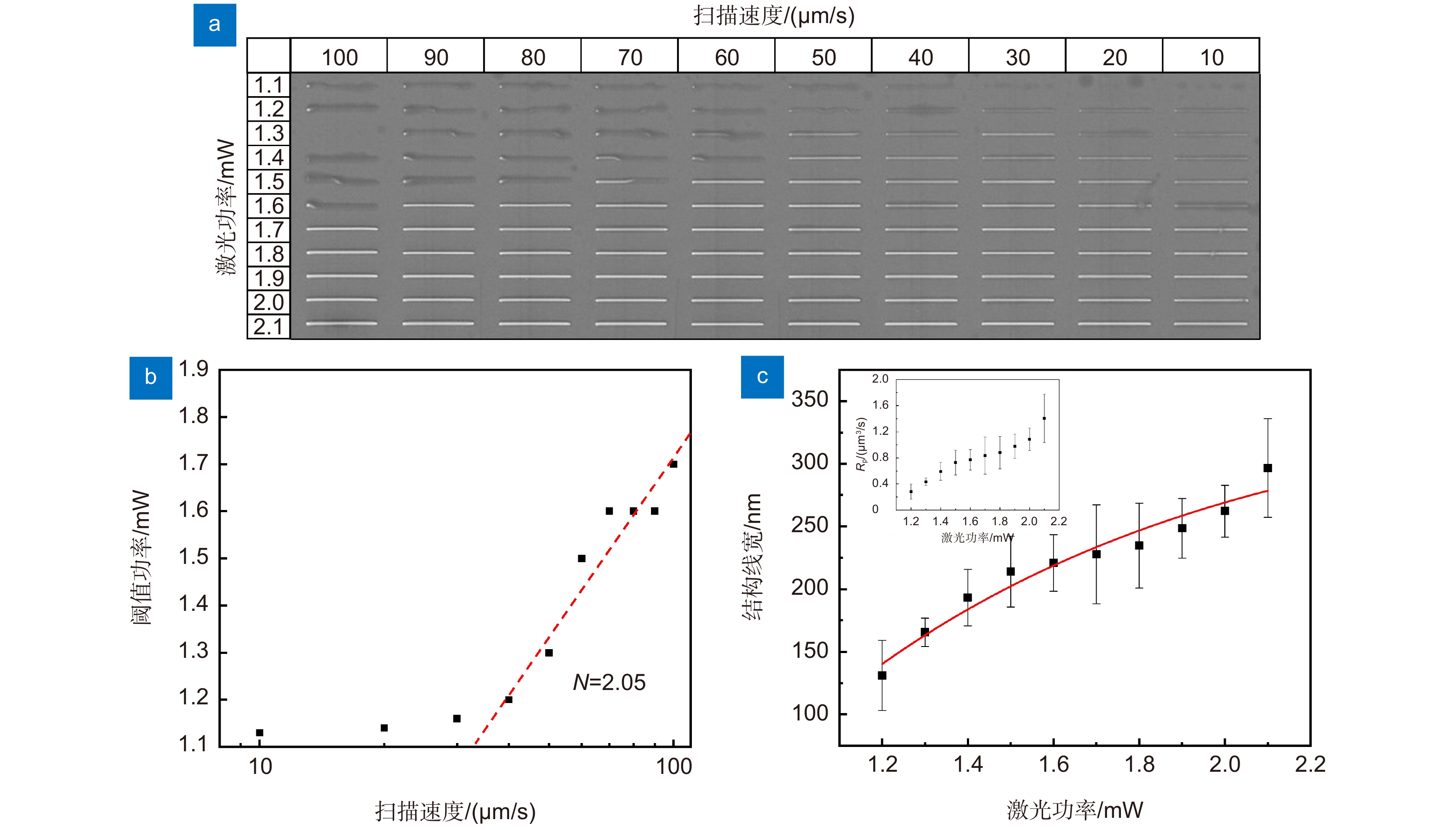
图 3 (a)不同激光功率、扫描速度下加工的单线结构SEM图片,其中VO2浓度为20 wt%;(b)基于20 wt% VO2光敏型复合材料在不同扫描速度下加工单线结构的激光阈值功率,激光阈值功率与扫描速度呈函数关系;(c)加工单线结构的结构线宽随功率变化图,其中扫描速度为20 μm/s,VO2浓度为20 wt%,插图为激光功率对聚合速率的影响
Figure 3. (a) SEM images of the single-line structures processed at different laser powers and scanning speeds, where the VO2 concentration is 20 wt%; (b) Laser threshold power of the processed single-line structures at different scanning speeds based on 20 wt% VO2 photosensitive composite materials. The laser threshold power is a function of the scanning speed; (c) The line width of the processed single-line structures changes with the power, where the scanning speed is 20 μm/s, the VO2 concentration is 20 wt%, and the embedded figure is the laser power versus the polymerization rate
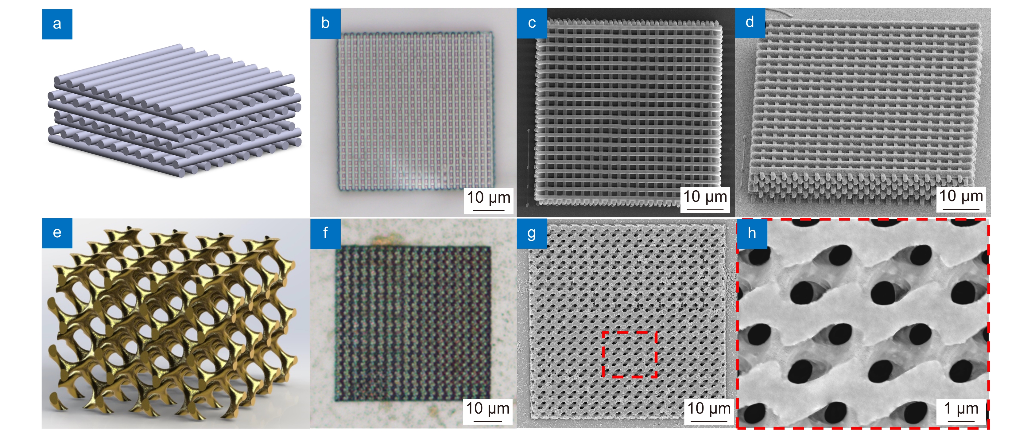
图 4 (a)三维层堆积结构模型示意图;(b-d)基于20 wt% VO2光敏型复合材料加工的三维层堆积结构,其中(b)为光学显微镜图片,(c)为SEM图片,(d)为SEM斜视图;(e)螺旋二十四面体模型示意图;(f-h)基于20 wt% VO2光敏型复合材料加工的螺旋二十四面体结构,其中(f)为光学显微镜图片,(g)为SEM图片,(h)为SEM放大图片
Figure 4. (a) Schematic diagram of the three-dimensional layer stacking structure model; (b-d) The three-dimensional layer stacking structure processed based on 20 wt% VO2 photosensitive composite material, where (b) is the optical microscope picture, (c) is the SEM picture, and (d) is the SEM oblique view; (e) Schematic diagram of the spiral icosahedral structure model; (f-h) Spiral icosahedral structure processed based on 20 wt% VO2 photosensitive composite material, where (f) is the optical microscope image, (g) is the SEM image, and (h) is the SEM enlarged image
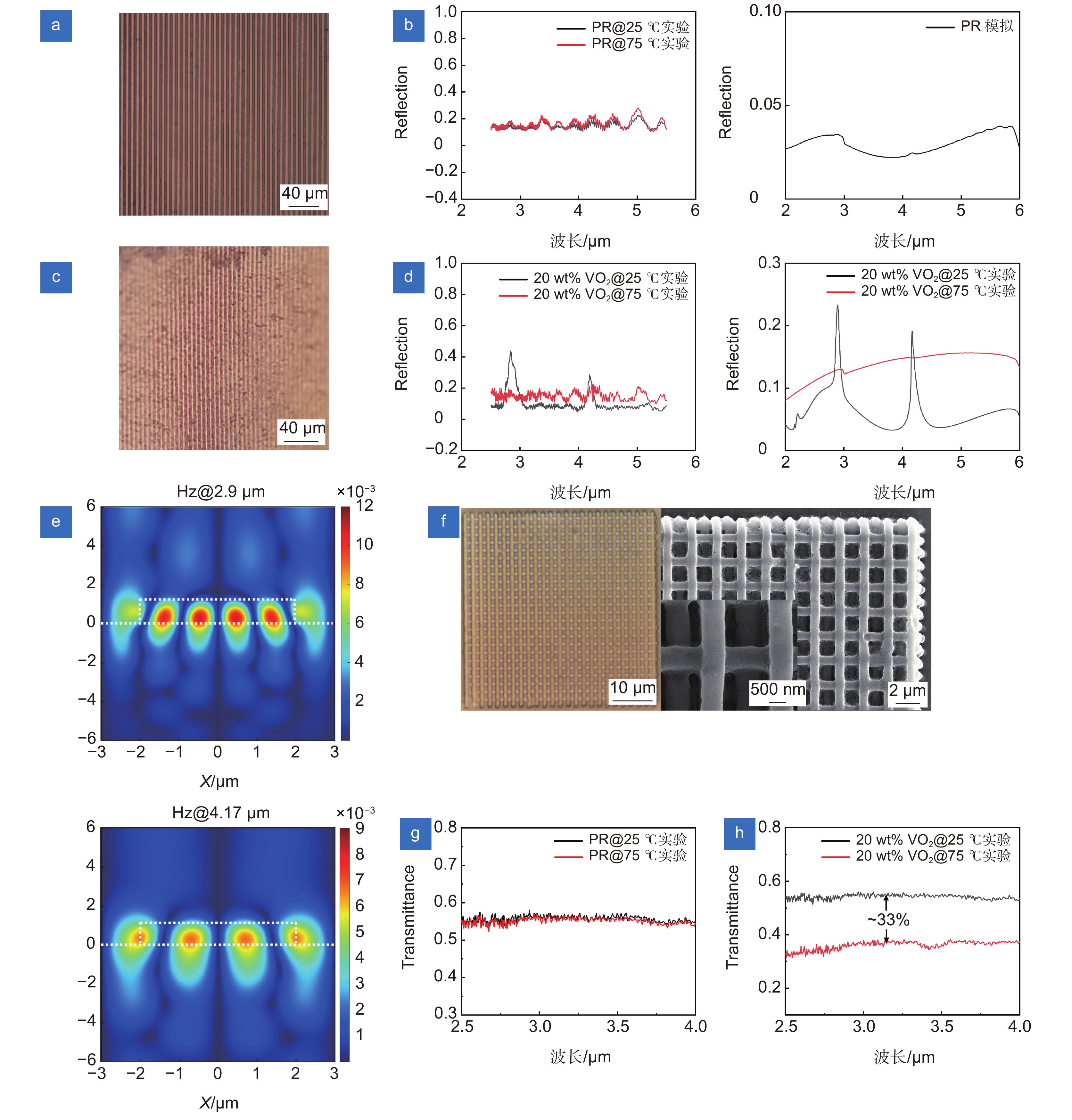
图 5 (a)纯光刻胶型一维光栅;(b)纯光刻胶型一维光栅器件升温前后的反射光谱,其中上图为测试数据,下图为模拟数据;(c) 20 wt% VO2型一维光栅;(d) 20 wt% VO2型一维光栅器件升温前后的反射光谱,其中上图为测试数据,下图为模拟数据;(e)单个周期的20 wt% VO2光栅XOZ平面的磁场z分量分布,其中上图光源波长为2.9 μm,下图光源波长为4.2 μm,白色虚线为单个周期光栅结构的截面轮廓;(f) 20 wt% VO2型woodpile结构;(g)纯光刻胶型woodpile结构升温前后的透射光谱;(h) 20 wt% VO2型woodpile结构升温前后的透射光谱,其中黑线为25 ℃,红线为75 ℃
Figure 5. (a) Pure photoresist-type one-dimensional grating; (b) Reflection spectra of pure photoresist-type one-dimensional grating device before and after heating, where the upper figure is the test data, and the lower figure is the simulated data; (c) 20 wt% VO2 type one-dimensional grating; (d) Reflection spectrum of 20 wt% VO2 type one-dimensional grating device before and after heating, where the upper figure is the test data, and the lower figure is the simulated data; (e) Distribution of the z component of the magnetic field in the XOZ plane of a single periodic 20 wt% VO2 grating, where the upper picture shows the light source wavelength of 2.9 μm, and the lower picture shows the light source wavelength of 4.2 μm, the white dotted line is the cross-sectional profile of a single periodic grating structure; (f) 20 wt% VO2 type woodpile structure; (g) Transmission spectra of pure photoresist woodpile structure before and after heating; (h) Transmission spectra of 20 wt% VO2 type woodpile structure before and after heating, where the black line is 25 ℃, and the red line is 75 ℃
-
[1] 李佳群, 闫剑锋, 李欣, 等. 透明介质材料的超快激光微纳加工研究进展[J]. 中国激光, 2021, 48(2): 0202019. doi: 10.3788/CJL202148.0202019
Li J Q, Yan J F, Li X, et al. Research advancement on ultrafast laser microprocessing of transparent dielectrics[J]. Chin J Lasers, 2021, 48(2): 0202019. doi: 10.3788/CJL202148.0202019
[2] Capel A J, Rimington R P, Lewis M P, et al. 3D printing for chemical, pharmaceutical and biological applications[J]. Nat Rev Chem, 2018, 2(12): 422−436. doi: 10.1038/s41570-018-0058-y
[3] Kiefer P, Hahn V, Nardi M, et al. Sensitive photoresists for rapid multiphoton 3D laser micro‐and nanoprinting[J]. Adv Opt Mater, 2020, 8(19): 2000895. doi: 10.1002/adom.202000895
[4] Mayer F, Ryklin D, Wacker I, et al. 3D two‐photon microprinting of nanoporous architectures[J]. Adv Mater, 2020, 32(32): 2002044. doi: 10.1002/adma.202002044
[5] Kawata S, Sun H B, Tanaka T, et al. Finer features for functional microdevices[J]. Nature, 2001, 412(6848): 697−698. doi: 10.1038/35089130
[6] Lay C L, Koh C S L, Lee Y H, et al. Two-photon-assisted polymerization and reduction: emerging formulations and applications[J]. ACS Appl Mater Interfaces, 2020, 12(9): 10061−10079. doi: 10.1021/acsami.9b20911
[7] Hua J G, Liang S Y, Chen Q D, et al. Free‐form micro‐optics out of crystals: femtosecond laser 3D sculpturing[J]. Adv Funct Mater, 2022, 32(26): 2200255. doi: 10.1002/adfm.202200255
[8] Corrielli G, Crespi A, Osellame R. Femtosecond laser micromachining for integrated quantum photonics[J]. Nanophotonics, 2021, 10(15): 3789−3812. doi: 10.1515/nanoph-2021-0419
[9] Ovsianikov A, Ostendorf A, Chichkov B N. Three-dimensional photofabrication with femtosecond lasers for applications in photonics and biomedicine[J]. Appl Surf Sci, 2007, 253(15): 6599−6602. doi: 10.1016/j.apsusc.2007.01.058
[10] Gansel J K, Thiel M, Rill M S, et al. Gold helix photonic metamaterial as broadband circular polarizer[J]. Science, 2009, 325(5947): 1513−1515. doi: 10.1126/science.1177031
[11] Jiang M L, Song S C, Li Y J, et al. 3D high precision laser printing of a flat nanofocalizer for subwavelength light spot array[J]. Opt Lett, 2021, 46(2): 356−359. doi: 10.1364/OL.413302
[12] Turner M D, Schröder-Turk G E, Gu M. Fabrication and characterization of three-dimensional biomimetic chiral composites[J]. Opt Express, 2011, 19(10): 10001−10008. doi: 10.1364/OE.19.010001
[13] McMillen B, Zhang B T, Chen K P, et al. Ultrafast laser fabrication of low-loss waveguides in chalcogenide glass with 0.65 dB/cm loss[J]. Opt Lett, 2012, 37(9): 1418−1420. doi: 10.1364/OL.37.001418
[14] Gan Z S, Cao Y Y, Evans R A, et al. Three-dimensional deep sub-diffraction optical beam lithography with 9 nm feature size[J]. Nat Commun, 2013, 4: 2061. doi: 10.1038/ncomms3061
[15] Yee D W, Lifson M L, Edwards B W, et al. Additive manufacturing of 3D‐architected multifunctional metal oxides[J]. Adv Mater, 2019, 31(33): 1901345. doi: 10.1002/adma.201901345
[16] Liu Y J, Wang H, Ho J, et al. Structural color three-dimensional printing by shrinking photonic crystals[J]. Nat Commun, 2019, 10(1): 4340. doi: 10.1038/s41467-019-12360-w
[17] Saha S K, Wang D E, Nguyen V H, et al. Scalable submicrometer additive manufacturing[J]. Science, 2019, 366(6461): 105−109. doi: 10.1126/science.aax8760
[18] Kelly B E, Bhattacharya I, Heidari H, et al. Volumetric additive manufacturing via tomographic reconstruction[J]. Science, 2019, 363(6431): 1075−1079. doi: 10.1126/science.aau7114
[19] Jia Y C, Wang S X, Chen F. Femtosecond laser direct writing of flexibly configured waveguide geometries in optical crystals: fabrication and application[J]. Opto-Electron Adv, 2020, 3(10): 190042. doi: 10.29026/oea.2020.190042
[20] 姜美玲, 张明偲, 李向平, 等. 超分辨光存储研究进展[J]. 光电工程, 2019, 46(3): 180649. doi: 10.12086/oee.2019.180649
Jiang M L, Zhang M S, Li X P, et al. Research progress of super-resolution optical data storage[J]. Opto-Electron Eng, 2019, 46(3): 180649. doi: 10.12086/oee.2019.180649
[21] Vyatskikh A, Ng R C, Edwards B, et al. Additive manufacturing of high-refractive-index, nanoarchitected titanium dioxide for 3D dielectric photonic crystals[J]. Nano Lett, 2020, 20(5): 3513−3520. doi: 10.1021/acs.nanolett.0c00454
[22] Frölich A, Fischer J, Zebrowski T, et al. Titania woodpiles with complete three-dimensional photonic bandgaps in the visible[J]. Adv Mater, 2013, 25(26): 3588−3592. doi: 10.1002/adma.201300896
[23] Hossain M M, Gu M. Broadband optical absorptions in inversed woodpile metallic photonic crystals[J]. Opt Mater Express, 2012, 2(8): 996−1002. doi: 10.1364/OME.2.000996
[24] Vyatskikh A, Delalande S, Kudo A, et al. Additive manufacturing of 3D nano-architected metals[J]. Nat Commun, 2018, 9(1): 593. doi: 10.1038/s41467-018-03071-9
[25] Wen H J, Song S C, Xie F, et al. Great chiral fluorescence from the optical duality of silver nanostructures enabled by 3D laser printing[J]. Mater Horiz, 2020, 7(12): 3201−3208. doi: 10.1039/D0MH01207F
[26] Xu B B, Xia H, Niu L G, et al. Flexible nanowiring of metal on nonplanar substrates by femtosecond‐laser‐induced electroless plating[J]. Small, 2010, 6(16): 1762−1766. doi: 10.1002/smll.201000511
[27] Xiong W, Liu Y, Jiang L J, et al. Laser‐directed assembly of aligned carbon nanotubes in three dimensions for multifunctional device fabrication[J]. Adv Mater, 2016, 28(10): 2002−2009. doi: 10.1002/adma.201505516
[28] Long J, Xiong W, Wei C Y R, et al. Directional assembly of ZnO nanowires via three-dimensional laser direct writing[J]. Nano Lett, 2020, 20(7): 5159−5166. doi: 10.1021/acs.nanolett.0c01378
[29] Xia H, Wang J, Tian Y, et al. Ferrofluids for fabrication of remotely controllable micro‐nanomachines by two‐photon polymerization[J]. Adv Mater, 2010, 22(29): 3204−3207. doi: 10.1002/adma.201000542
[30] 谢常青, 朱效立, 牛洁斌, 等. 微纳金属光学结构制备技术及应用[J]. 光学学报, 2011, 31(9): 0900128. doi: 10.3788/AOS201131.0900128
Xie C Q, Zhu X L, Niu J B, et al. Micro-and nano-metal structures fabrication technology and applications[J]. Acta Opt Sin, 2011, 31(9): 0900128. doi: 10.3788/AOS201131.0900128
[31] Fang W, Lei J, Zhang P D, et al. Multilevel phase supercritical lens fabricated by synergistic optical lithography[J]. Nanophotonics, 2020, 9(6): 1469−1477. doi: 10.1515/nanoph-2020-0064
[32] Golubev V G, Kurdyukov D A, Pevtsov A B, et al. Hysteresis of the photonic band gap in VO2 photonic crystal in the semiconductor-metal phase transition[J]. Semiconductors, 2002, 36(9): 1043−1047. doi: 10.1134/1.1507288
[33] Peter A P, Martens K, Rampelberg G, et al. Metal‐insulator transition in ALD VO2 ultrathin films and nanoparticles: morphological control[J]. Adv Funct Mater, 2015, 25(5): 679−686. doi: 10.1002/adfm.201402687
[34] Ke Y J, Wang S C, Liu G, et al. Vanadium dioxide: the multistimuli responsive material and its applications[J]. Small, 2018, 14(39): 1802025. doi: 10.1002/smll.201802025
[35] Hallman K A, Miller K J, Baydin A, et al. Sub‐picosecond response time of a hybrid VO2: silicon waveguide at 1550 nm[J]. Adv Opt Mater, 2021, 9(4): 2001721. doi: 10.1002/ADOM.202001721
[36] Wang H, Yang Y, Wang L P. Wavelength-tunable infrared metamaterial by tailoring magnetic resonance condition with VO2 phase transition[J]. J Appl Phys, 2014, 116(12): 123503. doi: 10.1063/1.4896525
[37] Han C R, Parrott E P J, Humbert G, et al. Broadband modulation of terahertz waves through electrically driven hybrid bowtie antenna-VO2 devices[J]. Sci Rep, 2017, 7(1): 12725. doi: 10.1038/s41598-017-13085-w
[38] Liu L, Kang L, Mayer T S, et al. Hybrid metamaterials for electrically triggered multifunctional control[J]. Nat Commun, 2016, 7: 13236. doi: 10.1038/ncomms13236
[39] Wang R, Yang W Y, Gao S, et al. Direct-writing of vanadium dioxide/polydimethylsiloxane three-dimensional photonic crystals with thermally tunable terahertz properties[J]. J Mater Chem C, 2019, 7(27): 8185−8191. doi: 10.1039/C8TC05759A
[40] Zhang Y B, Wu P H, Zhou Z G, et al. Study on temperature adjustable terahertz metamaterial absorber based on vanadium dioxide[J]. IEEE Access, 2020, 8: 85154−85161. doi: 10.1109/access.2020.2992700
[41] Hashemi M R M, Yang S H, Wang T Y, et al. Electronically-controlled beam-steering through vanadium dioxide metasurfaces[J]. Sci Rep, 2016, 6: 35439. doi: 10.1038/srep35439
[42] Driscoll T, Palit S, Qazilbash M M, et al. Dynamic tuning of an infrared hybrid-metamaterial resonance using vanadium dioxide[J]. Appl Phys Lett, 2008, 93(2): 024101. doi: 10.1063/1.2956675
[43] Taylor S, Yang Y, Wang L P. Vanadium dioxide based Fabry-Perot emitter for dynamic radiative cooling applications[J]. J Quant Spectrosc Radiat Transfer, 2017, 197: 76−83. doi: 10.1016/j.jqsrt.2017.01.014
[44] Kim M K, Lee D S, Yang Y H, et al. Switchable diurnal radiative cooling by doped VO2[J]. Opto-Electron Adv, 2021, 4(5): 200006. doi: 10.29026/oea.2021.200006
[45] Long L S, Taylor S, Wang L P. Enhanced infrared emission by thermally switching the excitation of magnetic polariton with scalable microstructured VO2 metasurfaces[J]. ACS Photonics, 2020, 7(8): 2219−2227. doi: 10.1021/acsphotonics.0c00760
[46] Premkumar P A, Toeller M, Radu I P, et al. Process study and characterization of VO2 thin films synthesized by ALD using TEMAV and O3 precursors[J]. ECS J Solid State Sci Technol, 2012, 1(4): P169−P174. doi: 10.1149/2.009204jss
[47] Ji R, Hua Y N, Chen K, et al. A switchable metalens based on active tri-layer metasurface[J]. Plasmonics, 2019, 14(1): 165−171. doi: 10.1007/s11468-018-0789-0
[48] Yan D X, Meng M, Li J S, et al. Vanadium dioxide-assisted broadband absorption and linear-to-circular polarization conversion based on a single metasurface design for the terahertz wave[J]. Opt Express, 2020, 28(20): 29843−29854. doi: 10.1364/OE.404829
[49] Ding F, Zhong S M, Bozhevolnyi S I. Vanadium dioxide integrated metasurfaces with switchable functionalities at terahertz frequencies[J]. Adv Opt Mater, 2018, 6(9): 1701204. doi: 10.1002/adom.201701204
[50] Liu C, Wang S C, Zhou Y, et al. Index-tunable anti-reflection coatings: Maximizing solar modulation ability for vanadium dioxide-based smart thermochromic glazing[J]. J Alloys Compd, 2018, 731: 1197−1207. doi: 10.1016/j.jallcom.2017.10.045
[51] 杨港, 郭迎辉, 蒲明博, 等. 基于相关性选择的微型计算光谱探测技术[J]. 光电工程, 2022, 49(10): 220130. doi: 10.12086/oee.2022.220130
Yang G, Guo Y H, Pu M B, et al. Miniature computational spectral detection technology based on correlation value selection[J]. Opto-Electron Eng, 2022, 49(10): 220130. doi: 10.12086/oee.2022.220130
[52] 王宝利, 朱振峰. 无机纳米粉体的团聚与表面改性[J]. 陶瓷学报, 2006, 27(1): 135−138. doi: 10.3969/j.issn.1000-2278.2006.01.028
Wang B L, Zhu Z F. Accumulation and surface modification of inorganic nano-particles[J]. J Ceram, 2006, 27(1): 135−138. doi: 10.3969/j.issn.1000-2278.2006.01.028
[53] Werdehausen D, Staude I, Burger S, et al. Design rules for customizable optical materials based on nanocomposites[J]. Opt Mater Express, 2018, 8(11): 3456−3469. doi: 10.1364/OME.8.003456
[54] Song S C, Li Y J, Yao Z F, et al. 3D laser nanoprinting of optically functionalized structures with effective-refractive-index tailorable TiO2 nanoparticle-doped photoresin[J]. Nanomaterials, 2021, 12(1): 55. doi: 10.3390/nano12010055
[55] 夏小兰, 曾宪智, 宋世超, 等. 基于柱矢量光调控的纵向超分辨率准球形多焦点阵列[J]. 光电工程, 2022, 49(11): 220109. doi: 10.12086/oee.2022.220109
Xia X L, Zeng X Z, Song S C, et al. Longitudinal super-resolution spherical multi-focus array based on column vector light modulation[J]. Opto-Electron Eng, 2022, 49(11): 220109. doi: 10.12086/oee.2022.220109
[56] 曹耀宇, 谢飞, 张鹏达, 等. 双光束超分辨激光直写纳米加工技术[J]. 光电工程, 2017, 44(12): 1133−1145. doi: 10.3969/j.issn.1003-501X.2017.12.001
Cao Y Y, Xie F, Zhang P D, et al. Dual‐beam super‐resolution direct laser writing nanofabrication technology[J]. Opto-Electron Eng, 2017, 44(12): 1133−1145. doi: 10.3969/j.issn.1003-501X.2017.12.001
[57] 张心正, 夏峰, 许京军. 激光超衍射加工机理与研究进展[J]. 物理学报, 2017, 66(14): 144207. doi: 10.7498/aps.66.144207
Zhang X Z, Xia F, Xu J J. The mechanisms and research progress of laser fabrication technologies beyond diffraction limit[J]. Acta Phys Sin, 2017, 66(14): 144207. doi: 10.7498/aps.66.144207
[58] Yu H Y, Ding H B, Zhang Q, et al. Three-dimensional direct laser writing of PEGda hydrogel microstructures with low threshold power using a green laser beam[J]. Light Adv Manuf, 2021, 2(1): 31−38. doi: 10.37188/lam.2021.003
[59] Gao W, Chao H, Zheng Y C, et al. Ionic carbazole-based water-soluble two-photon photoinitiator and the fabrication of biocompatible 3D hydrogel scaffold[J]. ACS Appl Mater Interfaces, 2021, 13(24): 27796−27805. doi: 10.1021/acsami.1c02227
-
 下载:
下载:
 点击扫一扫
点击扫一扫
图(6)
计量
- 文章访问数: 1923
- PDF下载数: 516
- 施引文献: 0


