
 E-mail Alert
 RSS
RSS
-
摘要:
中红外(2.5 µm~25 µm)波段包含许多重要的原子和分子共振峰,因此中红外超连续谱广泛应用于生物医学、光谱学和环境科学等领域。碲化镉(cadmium telluride, CdTe)在中红外波段具有超宽的透射光谱范围0.86 µm~25 µm,同时CdTe具有较大的三阶非线性系数,是实现中红外超连续谱的理想材料。本文设计并加工了一种基于CdTe为芯层、低折射率介质硫化镉为缓冲层、硅为衬底的波导。采用广义非线性薛定谔方程仿真了该波导以中心波长为5.5 µm中红外激光作为泵浦,能够实现4.1 µm~9.7 µm的超连续谱输出。实验中通过湿法刻蚀制作CdTe多晶波导,并采用中心波长为1030 nm,脉冲宽度为250 fs的激光器作为泵浦源,观察到在波导中发生明显的自相位调制而产生的光谱展宽。该工作为CdTe集成波导应用于中红外超连续谱及中红外波段的片上光学器件提供了新的可能。
Abstract:The mid-infrared (MIR) wavelength coincides with various molecular resonances and spectroscopy. It is a universal way to identify chemical and biological substances. Thus, the MIR supercontinuum generation (SCG) is widely used in biomedicine, spectroscopy, and environmental science. Cadmium telluride (CdTe) has an ultra-broad transparent spectral range, from 0.86 µm to 25 µm, and one of the largest third-order nonlinear coefficients. It makes CdTe become an excellent candidate for long-wavelength MIR on-chip SCG. As an important material of solar cells, there is a well-established thin film growth technology for CdTe. We designed a CdTe integrated waveguide on a low-refractive-index CdS film with a silicon substrate. The simulation results solved by the nonlinear Schrödinger equation manifest that the MIR SCG covering 4.1 µm to 9.7 µm can be generated from a 1 cm CdTe waveguide pumped by a 5.5 µm femtosecond laser. We experimentally fabricated the waveguide via the lithography and wet-etching techniques. The spectral broadening based on self-phase modulation from the large-core CdTe integrated waveguide is demonstrated by a femtosecond laser at the central wavelength of 1030 nm with a pulse width of 250 fs. The numerical simulations match well with the experimental results. These results pave the way for long-wavelength mid-infrared light sources and provide abundant new opportunities for MIR micro photonics.
-
Key words:
- integrated waveguide /
- supercontinuum /
- mid-infrared laser /
- ultrafast laser
-

-

图 1 片上集成CdTe波导的设计与仿真。(a) 基于CdTe/CdS/Si的波导三维结构图,CdTe波导的宽度(WCdTe)、高度(HCdTe)和CdS层的厚度(HCdS)分别为20 µm、8 µm和5 µm;(b) 不同厚度(3 µm、5 µm、10 µm、15 µm) CdS层造成的传输损耗;(c) 高和宽分别为20 µm和8 µm的CdTe内TE模式的总色散和模场束缚比例;(d) 以5.5 µm、15 kW脉冲作为泵浦,波导内产生的超连续谱光谱;(e)、(f) 分别为脉冲在长为1 cm的CdTe波导内传输的时域脉冲和频域光谱演化图
Figure 1. Design and simulation of the on-chip integrated CdTe waveguide. (a) The 3D structure diagram of the CdTe/CdS/Si waveguide. The width (WCdTe), height (
HCdTe), and thickness ( HCdS) of the CdTe waveguide are 20 µm, 8 µm, and 5 µm, respectively; (b) The propagation loss caused by the CdS layers with different thickness (3 µm, 5 µm, 10 µm, and 15 µm); (c) Total dispersion and mode confinement ratio of the TE mode in CdTe with 20 µm height and 8 µm width; (d) The SCG in the waveguide pumped with 5.5 µm, 15 kW pulse; (e) and (f) are the time-domain pulse and frequency-domain spectral evolution diagrams of the pulse propagated in a 1 cm-long CdTe waveguide, respectively 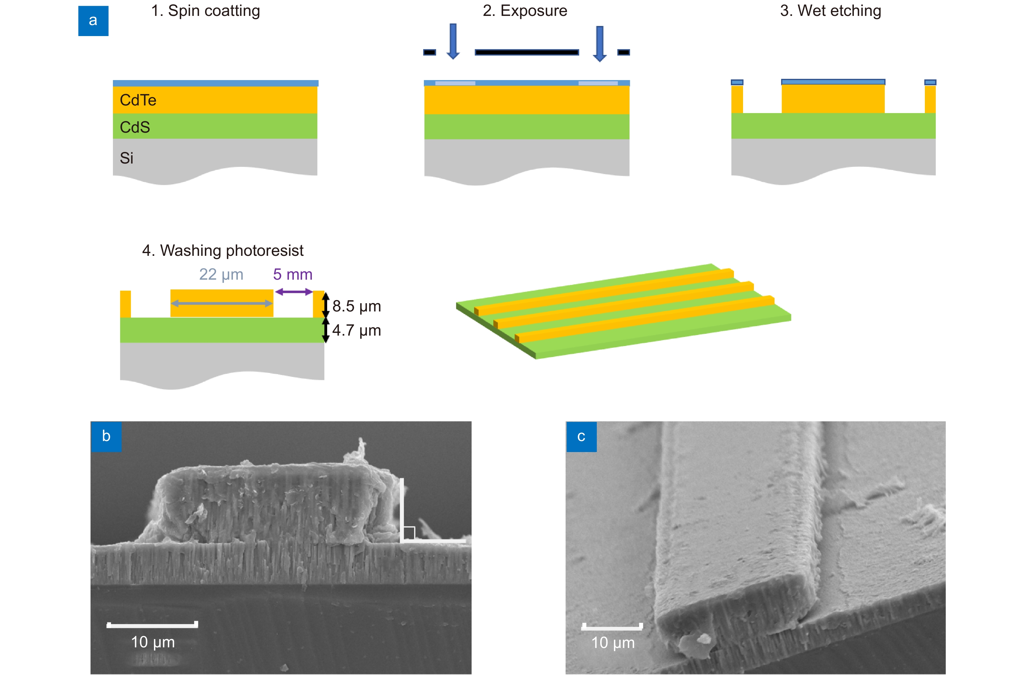
图 2 波导制作流程图和波导电镜表征图。(a) 波导制作流程图;(b) 波导端面形貌图,波导高度和宽度分别为8.5 µm和22 µm,波导侧壁与CdS层之间夹角为90°;(c) 波导侧面与顶面形貌图
Figure 2. Waveguide fabrication flow chart and scanning electron microscope images. (a) The waveguide fabrication flow chart; (b) The waveguide surface topography. The height and width of the waveguide are 8.5 µm and 22 µm, respectively. The angle between the side wall of the waveguide and the CdS layer is 90°; (c) The side and top topography of the waveguide
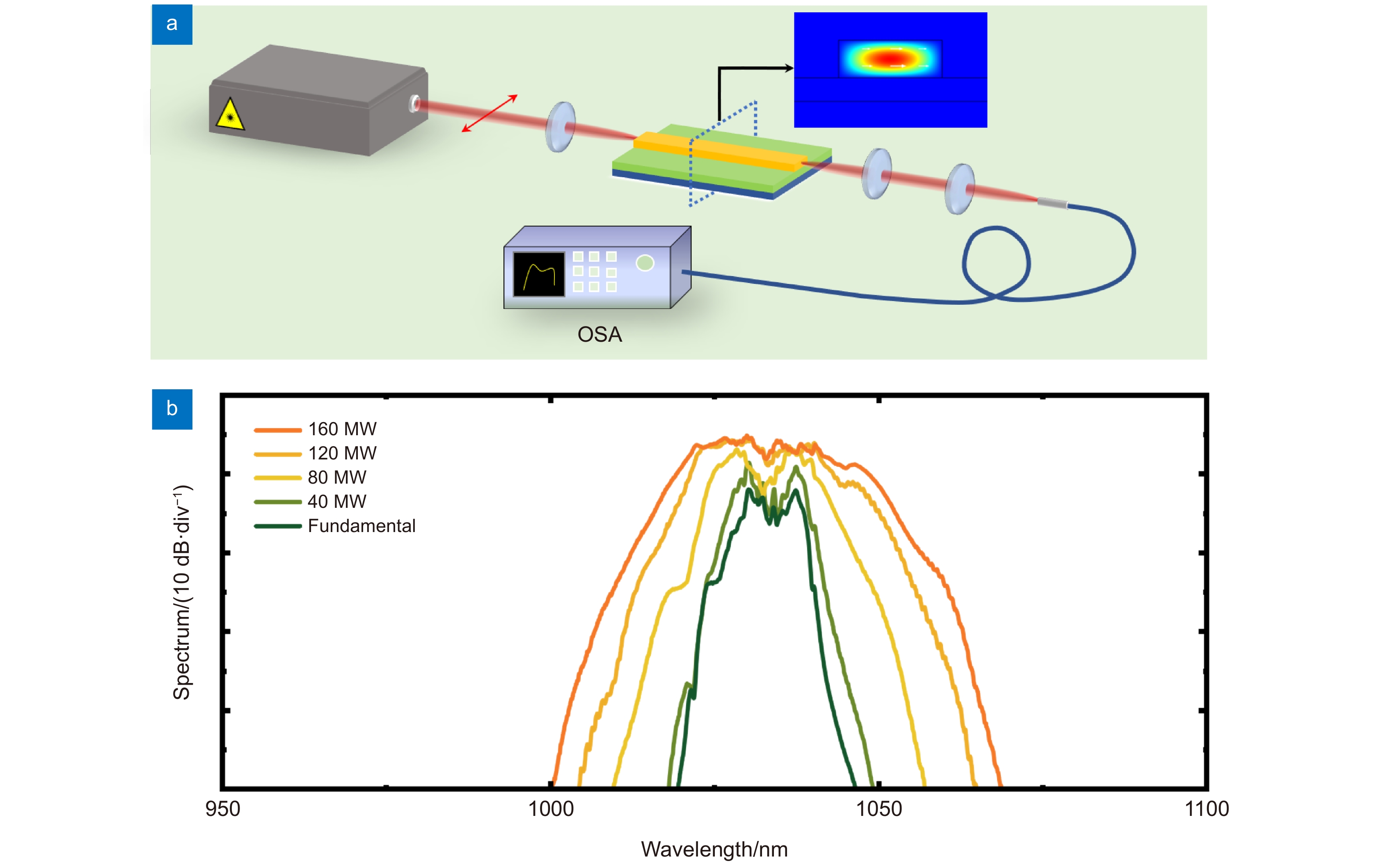
图 3 (a) 实验装置图,插图为波导内波长为1030 nm的TE模式图;(b) 不同泵浦功率下波导输出的展宽光谱
Figure 3. (a) The experimental setup diagram. The inset shows the field distribution of the TE mode at 1030 nm wavelength in the waveguide; (b) The broadened spectrum from the waveguide at different pump power
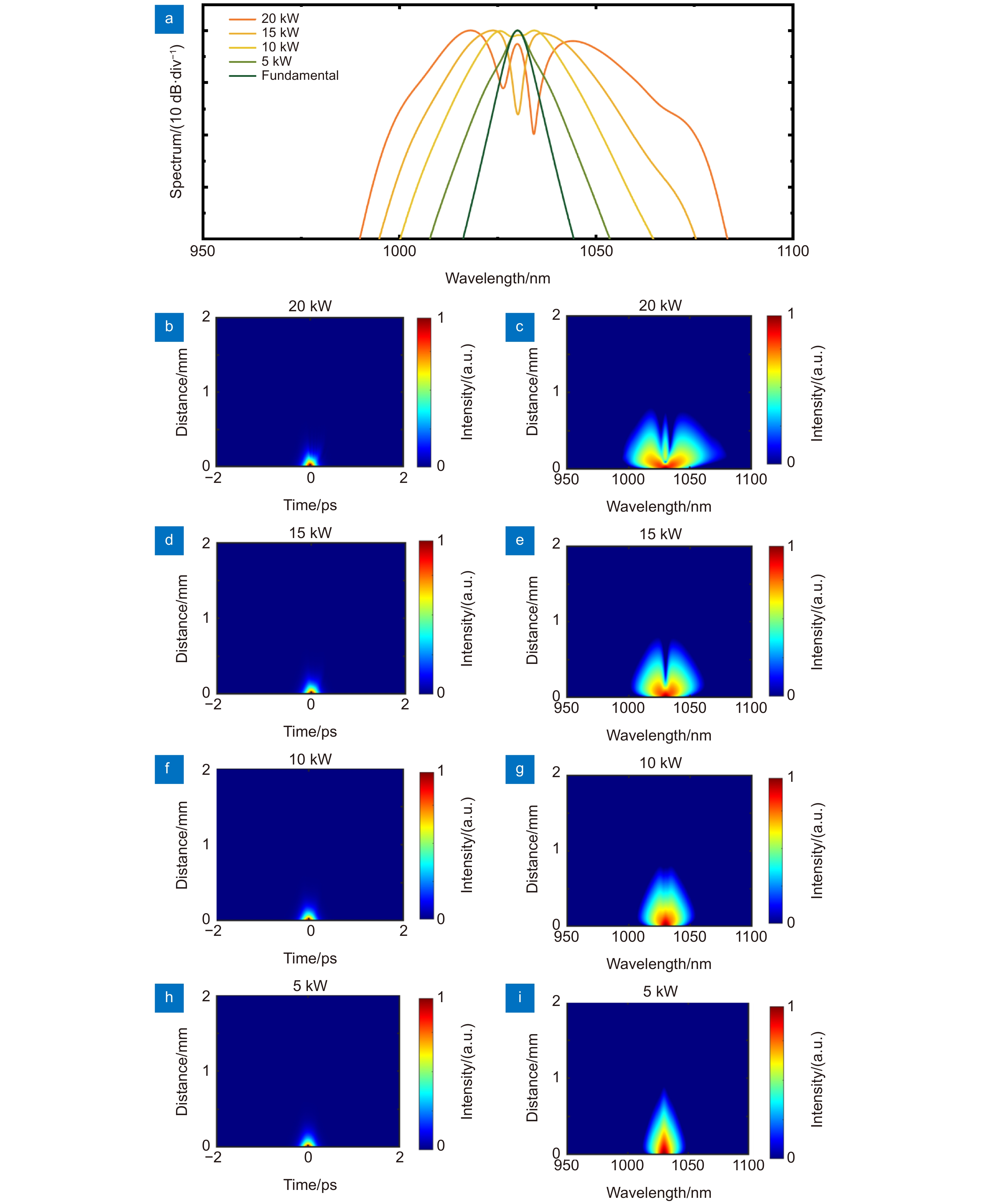
图 4 基于GNLSE求解在CdTe波导内的自相位调制导致的光谱展宽。 (a) 使用1030 nm波长进行泵浦,不同峰值功率(5 kW~20 kW)下波导的输出的光谱;(b), (d), (f), (h) 是超连续谱产生过程的时域演化图;(c), (e), (g), (i) 是超连续谱产生过程的频域演化图
Figure 4. Spectral broadening caused by self-phase modulation (SPM) in the CdTe waveguide based on GNLSE. (a) The output spectrum of the waveguide at different peak power (5 kW~20 kW) pumped at 1030 nm wavelength; (b), (d), (f), (h) The time-domain evolution diagrams of SCG process; (c), (e), (g), (i) The frequency-domain evolution diagrams of the SCG process
-
[1] Nakamoto K. Infrared and Raman Spectra of Inorganic and Coordination Compounds[M]. 6th ed. Hoboken: Wiley, 2009.
[2] Soref R. Mid-infrared photonics in silicon and germanium[J]. Nat Photonics, 2010, 4(8): 495−497. doi: 10.1038/nphoton.2010.171
[3] Hakala T, Suomalainen J, Kaasalainen S, et al. Full waveform hyperspectral LiDAR for terrestrial laser scanning[J]. Opt Express, 2012, 20(7): 7119−7127. doi: 10.1364/OE.20.007119
[4] Takara H, Ohara T, Yamamoto T, et al. Field demonstration of over 1000-channel DWDM transmission with supercontinuum multi-carrier source[J]. Electron Lett, 2005, 41(5): 270−271. doi: 10.1049/el:20057011
[5] Corrigan P, Martini R, Whittaker E A, et al. Quantum cascade lasers and the Kruse model in free space optical communication[J]. Opt Express, 2009, 17(6): 4355−4359. doi: 10.1364/OE.17.004355
[6] Nakasyotani T, Toda H, Kuri T, et al. Wavelength-division-multiplexed millimeter-waveband radio-on-fiber system using a supercontinuum light source[J]. J Lightwave Technol, 2006, 24(1): 404−410. doi: 10.1109/JLT.2005.859854
[7] Petrov V. Parametric down-conversion devices: the coverage of the mid-infrared spectral range by solid-state laser sources[J]. Opt Mater, 2012, 34(3): 536−554. doi: 10.1016/j.optmat.2011.03.042
[8] Zhao Z M, Wu B, Wang X S, et al. Mid-infrared supercontinuum covering 2.0–16 µm in a low-loss telluride single-mode fiber[J]. Laser Photonics Rev, 2017, 11(2): 1700005. doi: 10.1002/lpor.201700005
[9] Petersen C R, Møller U, Kubat I, et al. Mid-infrared supercontinuum covering the 1.4–13.3 μm molecular fingerprint region using ultra-high NA chalcogenide step-index fibre[J]. Nat Photonics, 2014, 8(11): 830−834. doi: 10.1038/nphoton.2014.213
[10] Yu Y, Gai X, Ma P, et al. Experimental demonstration of linearly polarized 2–10 µm supercontinuum generation in a chalcogenide rib waveguide[J]. Opt Lett, 2016, 41(5): 958−961. doi: 10.1364/OL.41.000958
[11] Wang P, Huang J P, Xie S R, et al. Broadband mid-infrared supercontinuum generation in dispersion-engineered As2S3-silica nanospike waveguides pumped by 2.8 µm femtosecond laser[J]. Photonics Res, 2021, 9(4): 630−636. doi: 10.1364/PRJ.415339
[12] Yu M J, Desiatov B, Okawachi Y, et al. Coherent two-octave-spanning supercontinuum generation in lithium-niobate waveguides[J]. Opt Lett, 2019, 44(5): 1222−1225. doi: 10.1364/OL.44.001222
[13] Iwakuni K, Okubo S, Tadanaga O, et al. Generation of a frequency comb spanning more than 3.6 octaves from ultraviolet to mid infrared[J]. Opt Lett, 2016, 41(17): 3980−3983. doi: 10.1364/OL.41.003980
[14] Hu Y T, Liang D, Beausoleil R G. An advanced III-V-on-silicon photonic integration platform[J]. Opto-Electron Adv, 2021, 4(9): 200094. doi: 10.29026/oea.2021.200094
[15] Guo H R, Herkommer C, Billat A, et al. Mid-infrared frequency comb via coherent dispersive wave generation in silicon nitride nanophotonic waveguides[J]. Nat Photonics, 2018, 12(6): 330−335. doi: 10.1038/s41566-018-0144-1
[16] Nader N, Maser D L, Cruz F C, et al. Versatile silicon-waveguide supercontinuum for coherent mid-infrared spectroscopy[J]. APL Photonics, 2018, 3(3): 036102. doi: 10.1063/1.5006914
[17] Singh N, Hudson D D, Yu Y, et al. Midinfrared supercontinuum generation from 2 to 6 µm in a silicon nanowire[J]. Optica, 2015, 2(9): 797−802. doi: 10.1364/OPTICA.2.000797
[18] Sinobad M, Monat C, Davies B L, et al. Mid-infrared octave spanning supercontinuum generation to 8.5 µm in silicon-germanium waveguides[J]. Optica, 2018, 5(4): 360−366. doi: 10.1364/OPTICA.5.000360
[19] Della Torre A, Sinobad M, Armand R, et al. Mid-infrared supercontinuum generation in a low-loss germanium-on-silicon waveguide[J]. APL Photonics, 2021, 6(1): 016102. doi: 10.1063/5.0033070
[20] Ballester M M, Lafforgue C, Frigerio J, et al. On-chip mid-infrared supercontinuum generation from 3 to 13 µm wavelength[J]. ACS Photonics, 2020, 7(12): 3423−3429. doi: 10.1021/acsphotonics.0c01232
[21] Palik E D. Handbook of Optical Constants of Solids[M]. San Diego: Academic Press, 1998.
[22] Tatsuura S, Matsubara T, Mitsu H, et al. Cadmium telluride bulk crystal as an ultrafast nonlinear optical switch[J]. Appl Phys Lett, 2005, 87(25): 251110. doi: 10.1063/1.2151256
[23] Sheik-Bahae M, Hagan D J, van Stryland E W. Dispersion and band-gap scaling of the electronic Kerr effect in solids associated with two-photon absorption[J]. Phys Rev Lett, 1990, 65(1): 96−99. doi: 10.1103/PhysRevLett.65.96
[24] Gaeta A L, Lipson M, Kippenberg T J. Photonic-chip-based frequency combs[J]. Nat Photonics, 2019, 13(3): 158−169. doi: 10.1038/s41566-019-0358-x
[25] Xin C G, Zhang J B, Xu P Z, et al. Self-phase modulation in single CdTe nanowires[J]. Opt Express, 2019, 27(22): 31800−31809. doi: 10.1364/OE.27.031800
[26] Long Z, Yang H, Li Y, et al. Cadmium telluride waveguide for coherent MIR supercontinuum generation covering 3.5–20 µm[J]. Opt Express, 2022, 30(2): 2265−2277. doi: 10.1364/OE.446801
[27] Paudel N R, Wieland K A, Compaan A D. Ultrathin CdS/CdTe solar cells by sputtering[J]. Solar Energy Mater Solar Cells, 2012, 105: 109−112. doi: 10.1016/j.solmat.2012.05.035
[28] Chenault D B, Chipman R A. Infrared birefringence spectra for cadmium sulfide and cadmium selenide[J]. Appl Opt, 1993, 32(22): 4223−4227. doi: 10.1364/AO.32.004223
[29] DeBell A G, Dereniak E L, Harvey J, et al. Cryogenic refractive indices and temperature coefficients of cadmium telluride from 6 µm to 22 µm[J]. Appl Opt, 1979, 18(18): 3114−3115. doi: 10.1364/AO.18.003114
[30] Marple D T F. Refractive index of ZnSe, ZnTe, and CdTe[J]. J Appl Phys, 1964, 35(3): 539−542. doi: 10.1063/1.1713411
[31] Edwards D F, Ochoa E. Infrared refractive index of silicon[J]. Appl Opt, 1980, 19(24): 4130−4131. doi: 10.1364/AO.19.004130
[32] Agrawal G P. Nonlinear Fiber Optics[M]. 5th ed. Amsterdam: Academic Press, 2013.
[33] Kraft D, Thissen A, Broetz J, et al. Characterization of tellurium layers for back contact formation on close to technology treated CdTe surfaces[J]. J Appl Phys, 2003, 94(5): 3589−3598. doi: 10.1063/1.1597757
[34] Bradley J D B, Evans C C, Choy J T, et al. Submicrometer-wide amorphous and polycrystalline anatase TiO2 waveguides for microphotonic devices[J]. Opt Express, 2012, 20(21): 23821−23831. doi: 10.1364/OE.20.023821
-
 下载:
下载:
 点击扫一扫
点击扫一扫
图(4)
计量
- 文章访问数: 2698
- PDF下载数: 600
- 施引文献: 0


