
 E-mail Alert
 RSS
RSS
-
摘要:
随着军用光电技术的快速发展,隐身技术在现代作战体系中的作用日趋重要,其中,隐身材料对于提高隐身性能至关重要。本文针对红外隐身材料,重点从单波段的红外隐身、多波段兼容的红外隐身、动态的红外隐身三方面综述了国内外红外隐身材料的研究进展,就微纳结构大面积柔性加工方法进行了深入分析。归纳了当前红外隐身材料存在的主要问题,并展望了未来发展趋势。未来,红外隐身材料将向着高强度、大面积、柔性化、智能化的新型结构和材料方向进一步发展,实现高性能的隐身功能。
Abstract:With the rapid development of military optoelectronic technology, the role of stealth technology in modern combat systems is becoming more and more important, among which, stealth materials are crucial to improve stealth performance. We focus on infrared stealth materials and review the research progress of domestic and foreign infrared stealth materials from three aspects including single-band infrared stealth, multi-band compatible infrared stealth, and dynamic infrared stealth, and provide an in-depth analysis on the large-area flexible processing methods for micro-nano structures. The main problems of current infrared stealth materials are summarized and the future development trend is foreseen. In the future, to achieve high-performance stealth functions, new infrared stealth materials will further develop in the direction of high strength, large area, flexibility, and intelligence.
-
Key words:
- infrared stealth /
- metasurface /
- F-P cavity structure /
- photonic crystal /
- micro-nano fabrication
-
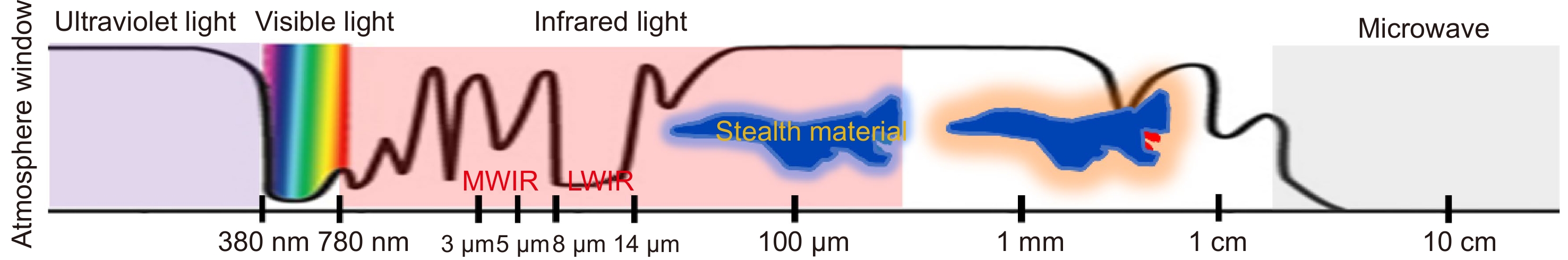
Overview: With the rapid development of military optoelectronic technology, the role of stealth technology in modern combat systems is becoming more and more important, in which stealth materials are essential to improve stealth performance. Infrared stealth is to tune the infrared radiation signal characteristics of the target to become the smallest difference from the background. The target will be invisible in the background and can not be identified through the infrared imaging equipment.
Starting from the background of infrared stealth technology, we introduce the classification of stealth technology and the progress of domestic and foreign infrared stealth materials from three aspects including single-band infrared stealth, multi-band compatible infrared stealth, and dynamic infrared stealth, and provide an in-depth analysis on the large-area flexible processing methods for micro-nano structures. Compared with single-band infrared stealth, multi-band compatible infrared stealth based on the photonic crystal, Fabry-Perot cavity structure, and metasurface, dynamic infrared stealth has higher freedom of spectral modulation. With the development of advanced micro-nano processing technology, metasurface is expected to become the first choice for new infrared stealth in the future due to its ultra-high freedom spectral modulation, ultra-thin subwavelength structures, etc. In addition, we have conducted an in-depth analysis of flexible processing methods for large areas of micro and nano structures.
Finally, based on the summary and reflection of the research work, the development of new infrared stealth materials will be further prospected. 1) High-strength direction development. In some stealth material application scenarios such as aircraft, vehicles, tanks, and other weaponry, the material will function in extreme environments. Therefore, the new infrared stealth materials have good mechanical properties, high-temperature resistance, corrosion resistance, impact resistance, etc. 2) Large-area direction development. In actual applications, the target to be stealthy is from centimeter-level to meter-level applications, so a large area of new infrared stealth materials is the inevitable trend of future development. 3) Flexible direction development. No matter the stealth target is equipment parts or clothing wear, achieving conformal stealth is a key part of stealth material development. 4) Intelligent direction development. Due to the continuous development and integration of multi-band detection technology and the harsh requirements of the actual environment, the realization of real-time dynamic multi-band intelligent stealth is a major demand for stealth technology.
-

-
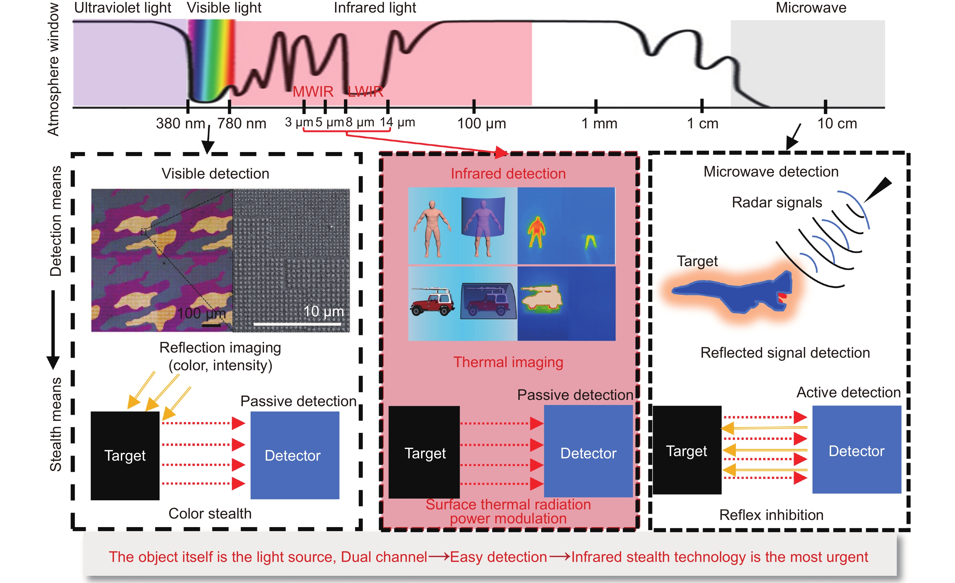
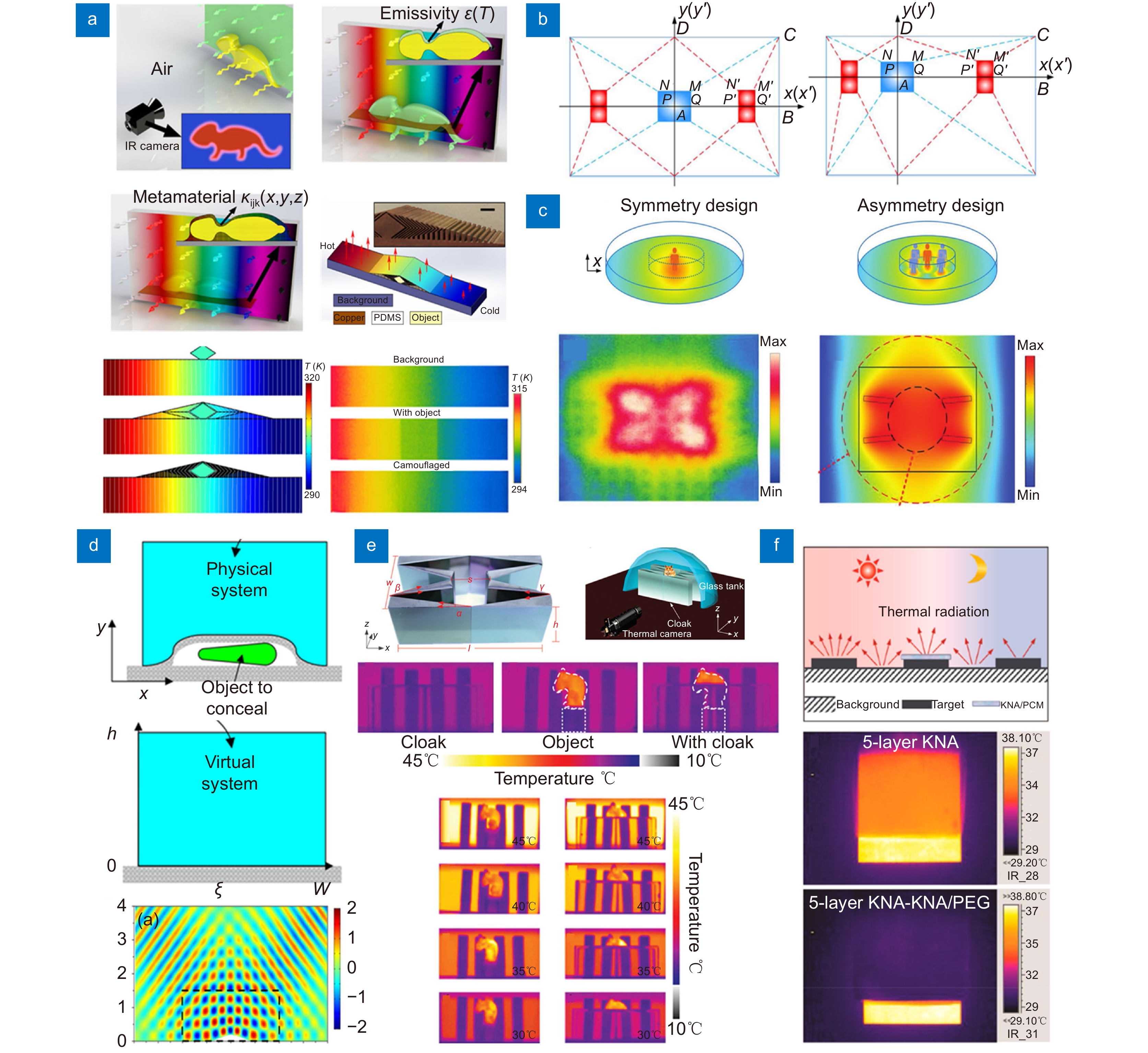
图 2 基于温度调控的红外隐身研究。(a) 结构化热表面[12];(b), (c) 虚拟目标的视觉混淆[13-14] ;(d) 隐身斗篷[15];(e) 远红外单向隐身斗篷[16];(f) 基于热绝缘材料的红外隐身[17]
Figure 2. Infrared stealth studies based on temperature modulation. (a) Structured thermal surfaces[12]; (b), (c) Visual obfuscation of virtual targets[13-14]; (d) Stealth cloak[15]; (e) Far-infrared unidirectional stealth cloak[16]; (f) Infrared stealth based on thermally insulating materials[17]
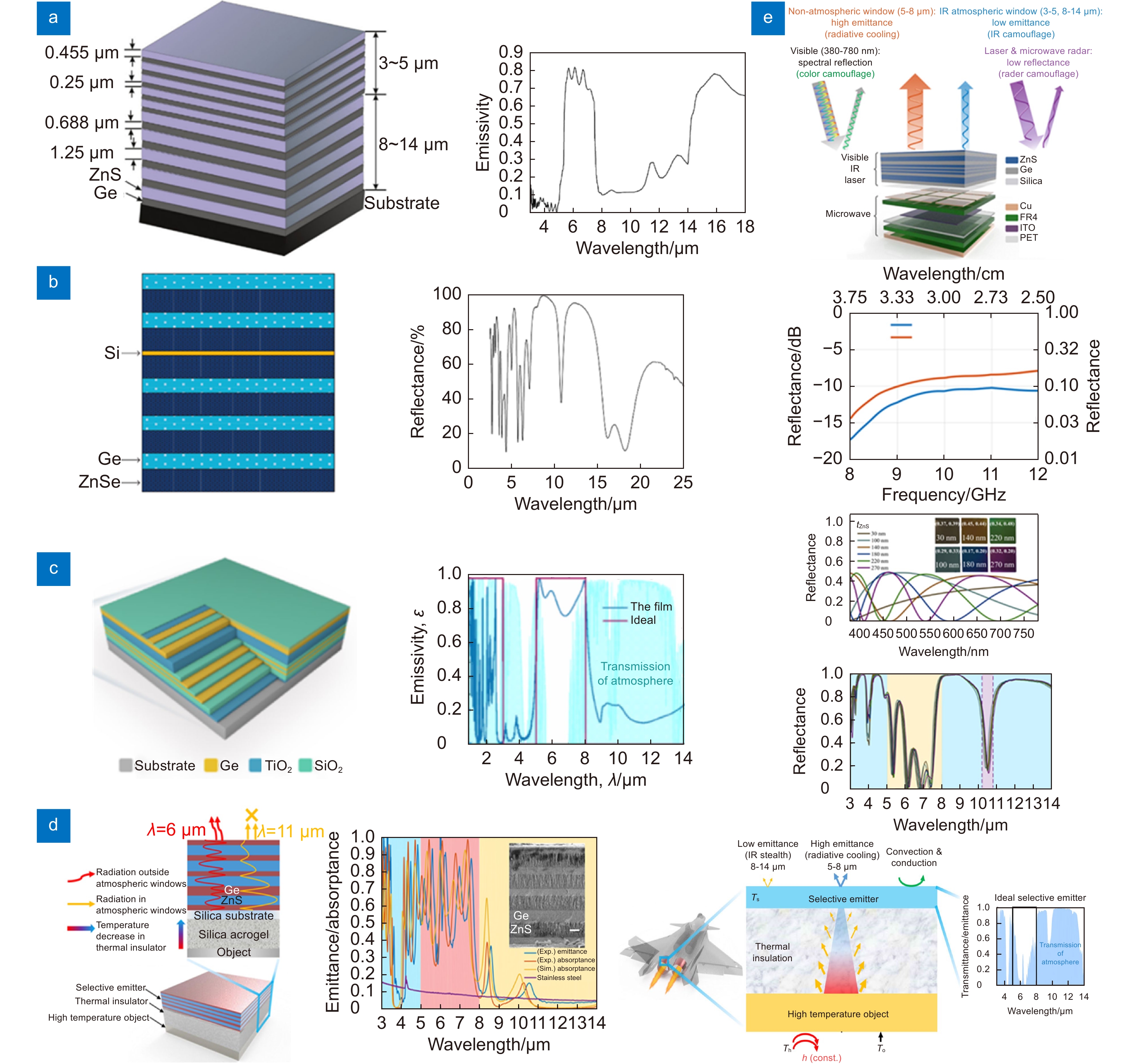
图 3 基于光子晶体结构的红外隐身研究。(a) Ge/ZnS光子晶体结构[21];(b) Ge、ZnSe、Si光子晶体结构[22];(c) SiO2、TiO2、Ge交替结构[23];(d) Ge/ZnS光子晶体结构[24];(e) 多光谱兼容光子晶体结构[25]
Figure 3. Infrared stealth research based on photonic crystal structures. (a) Ge/ZnS photonic crystals[21]; (b) Ge, ZnSe, Si photonic crystals[22]; (c) SiO2, TiO2, Ge alternating multilayer structures[23]; (d) Ge/ZnS photonic crystal structures[24]; (e) Multispectral compatible photonic crystal structures[25]
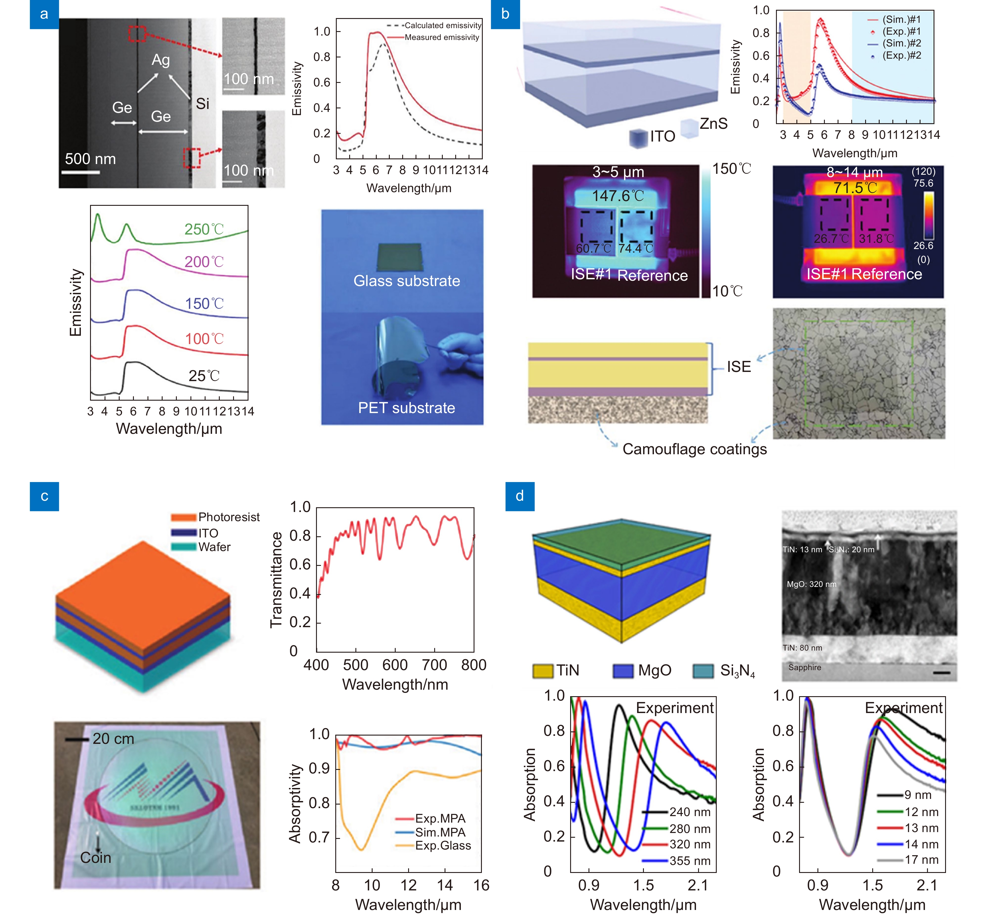
图 4 基于F-P腔结构的红外隐身研究。(a) Ag/Ge多层膜的红外隐身选择性发射器[27];(b) 氧化铟锡透明导电膜和硫化锌介电膜复合四层结构[28] ;(c) 光刻胶和氧化铟锡四层交替结构[29];(d) Si3N4-TiN-MgO-TiN四层结构[30]
Figure 4. Infrared stealth research based on F-P cavity structures. (a) Infrared stealth selective emitter with Ag/Ge multilayer films [27]; (b) Composite four-layer structure with transparent conductive films of indium tin oxide and dielectric films of zinc sulfide [28]; (c) Alternating four-layer structure with photoresist and indium tin oxide [29]; (d) Si3N4-TiN-MgO-TiN four-layer structures[30]
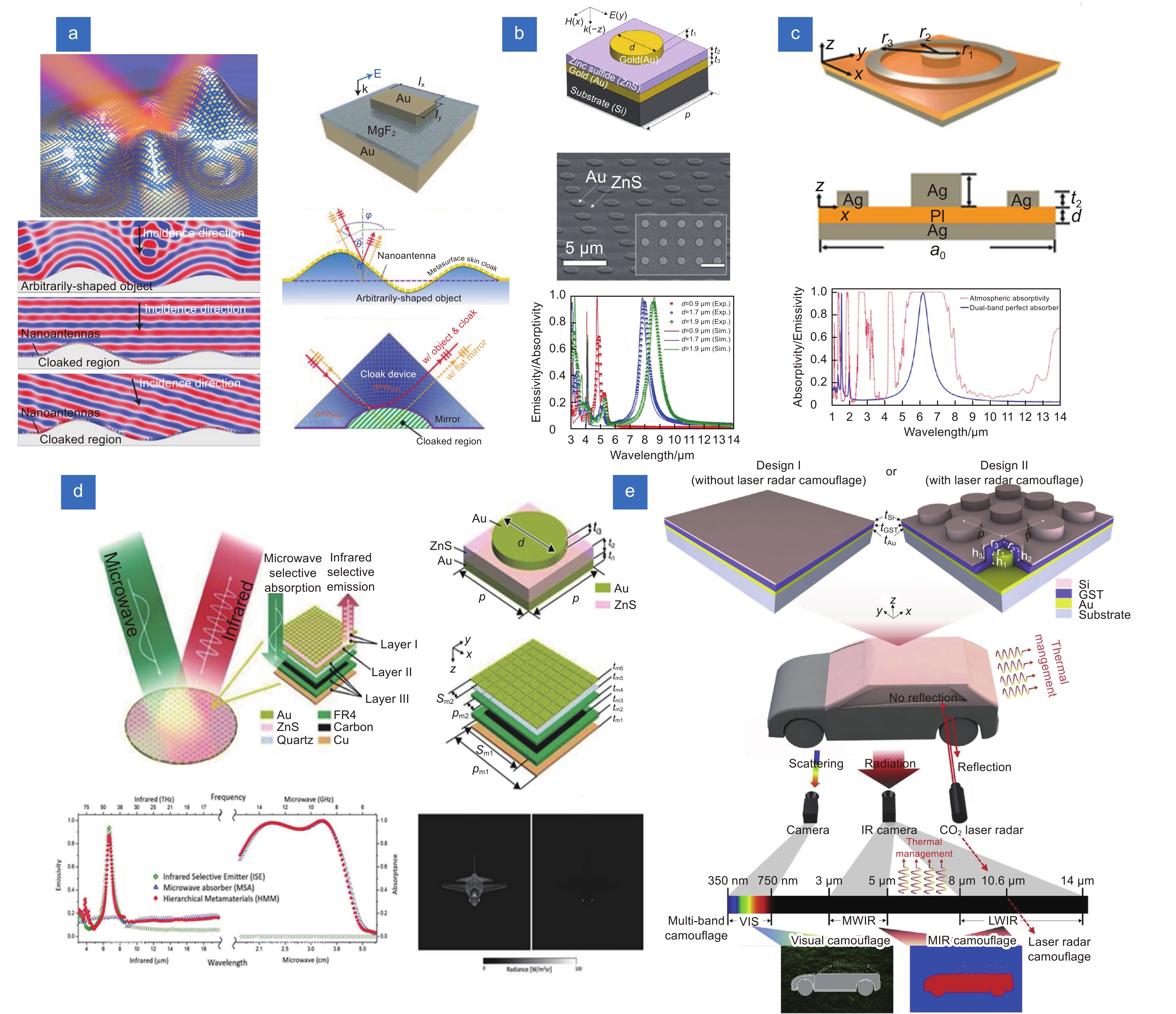
图 5 基于超构表面隐身材料的研究。(a) 超表面隐身地毯[53];(b) 圆盘超表面[54];(c) 圆环超表面[55];(d) 兼容红外和微波隐身的分层超表面[56];(e) 兼容可见光、红外、红外激光隐身的超表面[57]
Figure 5. Infrared stealth research based on metasurface structures. (a) Metasurface stealth carpet[53]; (b) Disc metasurface [54]; (c) Circular metasurface[55]; (d) Metasurface compatible with IR and microwave stealth[56]; (e) Metasurface compatible with visible, infrared, and laser stealth[57]
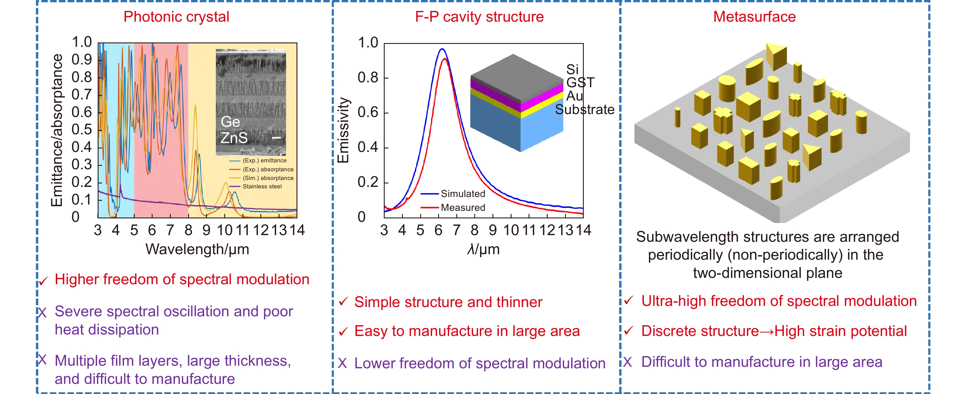
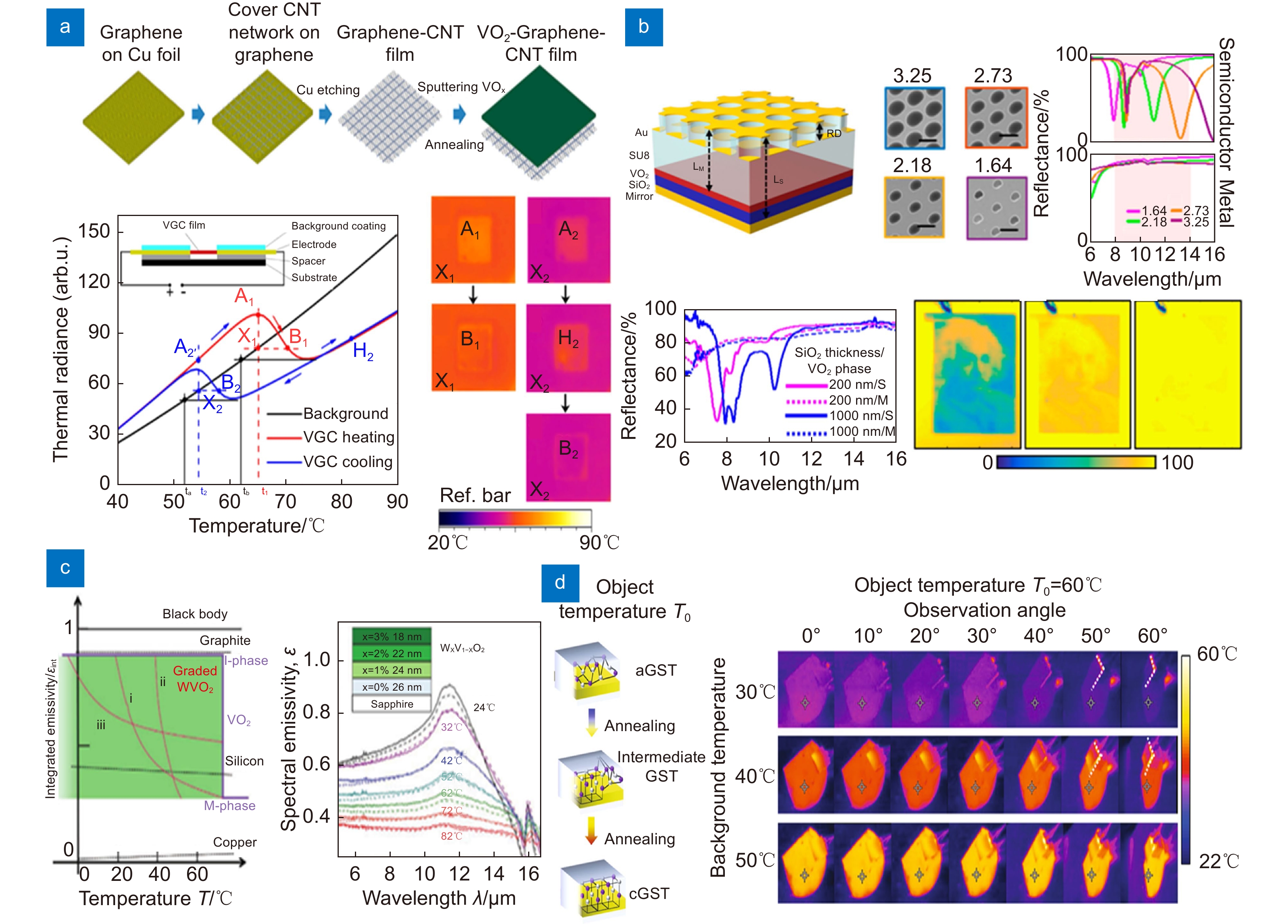
图 7 结合相变材料动态调控隐身材料应用实例。(a) VO2、石墨烯、碳纳米管三层结构隐身装置[77];(b) 多层的空腔耦合的红外吸收器[78];(c) 钨掺杂的二氧化钒的薄膜结构[79];(d) GST-Au两层结构[80]
Figure 7. Examples of combined phase change materials for dynamic modulation of stealth materials applications. (a) VO2, graphene, and carbon nanotube trilayer structure stealth device[77]; (b) Multilayer cavity-coupled IR absorber[78]; (c) Thin film structure of tungsten-doped vanadium dioxide[79]; (d) GST-Au two-layer structure[80]
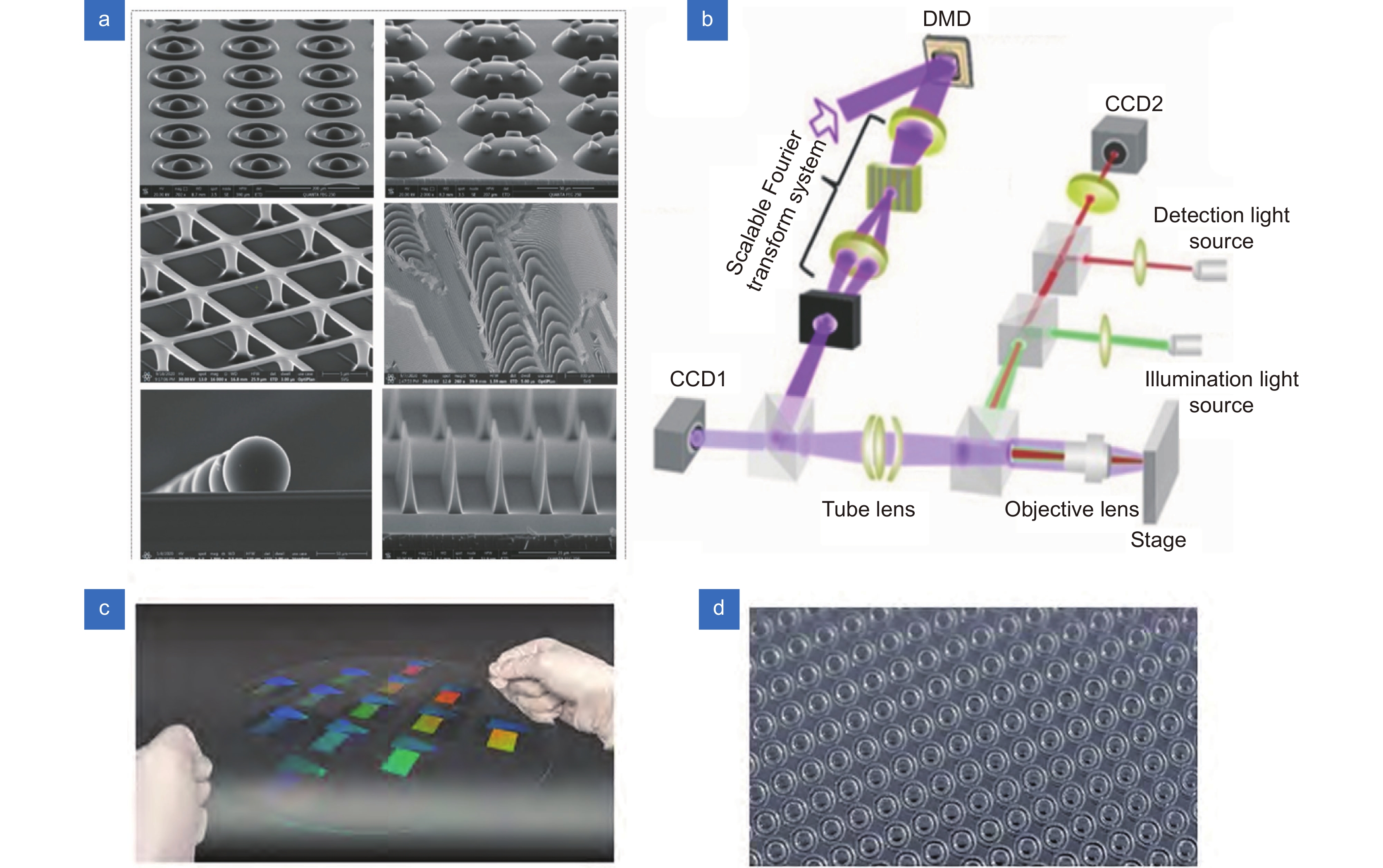
图 8 (a) 利用3D激光直写技术加工出的复杂图形;(b) 紫外连续变频光刻技术光路[89];(c) EVG 770NT制备300 mm模板;(d) GL SR300300 mm大面积母模板[90]
Figure 8. (a) Complex pattern processed by 3D laser direct writing technology; (b) UV continuous frequency lithography optical path[89]; (c) 300 mm stencil prepared by EVG 770NT; (d) GL SR300300 mm large area master stencil[90]
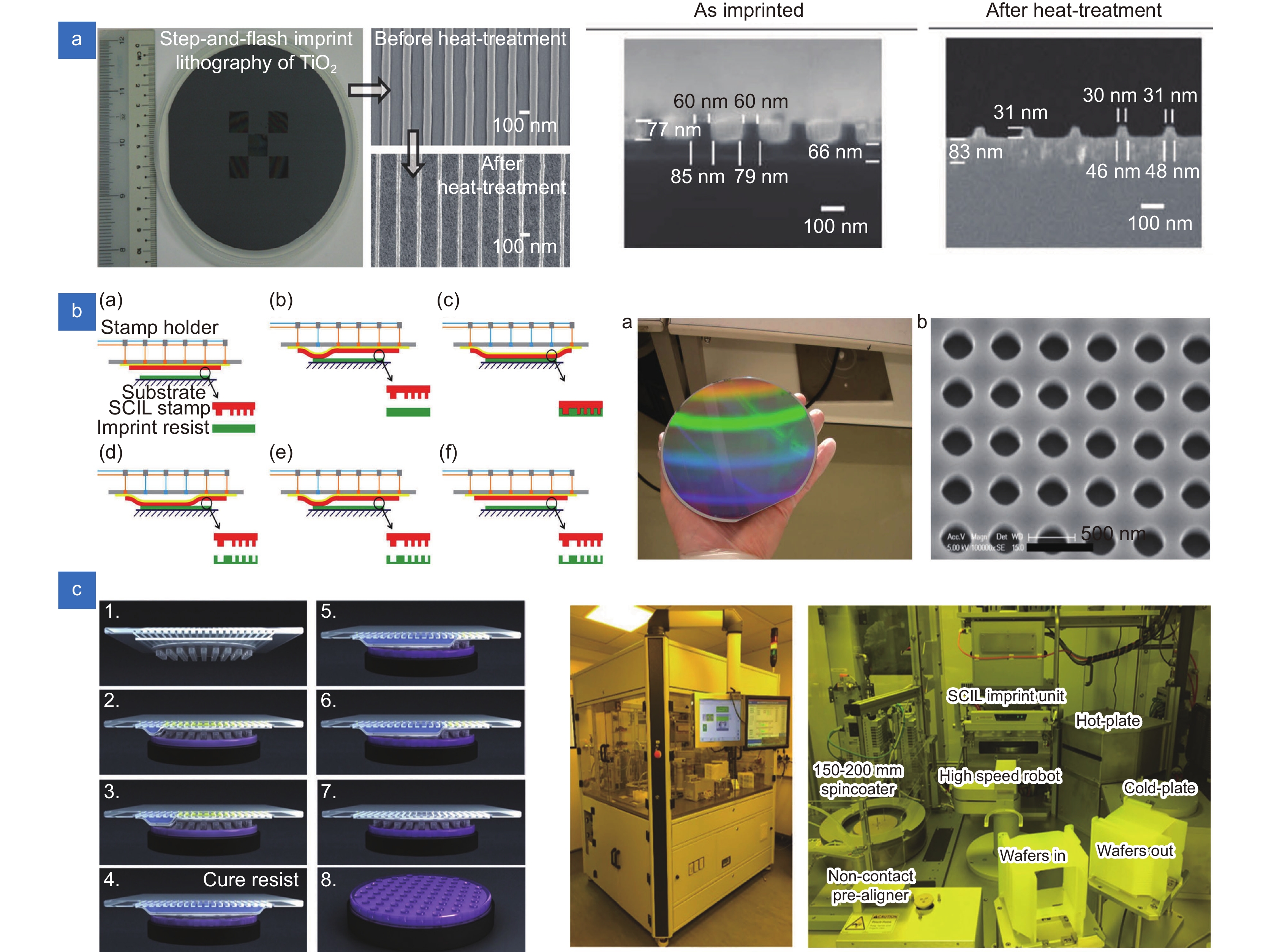
图 9 纳米压印技术研究示例。(a) 步进闪光压印技术压印的宽度为100 nm的光栅[93];(b) UV-SCIL平板压印[94];(c) 晶圆级区域上实现亚10 nm的分辨率[95]
Figure 9. Examples of nanoimprinting technique studies. (a) Grating with a width of 100 nm embossed by step flash embossing technique[93]; (b) UV-SCIL plate embossing[94]; (c) Sub-10 nm resolution achieved on wafer-level area[95]

表 1 文献报道的超构表面结构面积和柔性对比
Table 1. Comparison of structural area and flexibility of metasurfaces in the reported literature
 下载: 导出CSV
-
[1] Bahret W F. The beginnings of stealth technology[J]. IEEE Trans Aerosp Electron Syst, 1993, 29(4): 1377−1385. doi: 10.1109/7.259548
[2] Li W, Fan S H. Nanophotonic control of thermal radiation for energy applications [Invited][J]. Opt Express, 2018, 26(12): 15995−16021. doi: 10.1364/OE.26.015995
[3] Rogalski A. Recent progress in infrared detector technologies[J]. Infrared Phys Technol, 2011, 54(3): 136−154. doi: 10.1016/j.infrared.2010.12.003
[4] Sun X C, Zhang T X, Li M. Moving point target detection using temporal variance filter in IR imagery[J]. Proc SPIE, 2007, 6786: 67861Z. doi: 10.1117/12.749185
[5] Lu J H, Wang R F. The implementation method and the development tendency of infrared stealth technology[J]. Proc SPIE, 2015, 9674: 96741V. doi: 10.1117/12.2199702
[6] Moghimi M J, Lin G Y, Jiang H R. Broadband and ultrathin infrared stealth sheets[J]. Adv Eng Mater, 2018, 20(11): 1800038. doi: 10.1002/adem.201800038
[7] Kim J, Park C, Hahn J W. Metal–semiconductor–metal metasurface for multiband infrared stealth technology using camouflage color pattern in visible range[J]. Adv Opt Mater, 2022, 10(6): 2101930. doi: 10.1002/adom.202101930
[8] 付伟. 红外隐身原理及其应用技术[J]. 红外与激光工程, 2002, 31(1): 88−93. doi: 10.3969/j.issn.1007-2276.2002.01.021
Fu W. Principle and application technology of IR stealth[J]. Infrared Laser Eng, 2002, 31(1): 88−93. doi: 10.3969/j.issn.1007-2276.2002.01.021
[9] 陈翾, 袁江涛, 杨立. 地面目标红外特性及其隐身技术研究[J]. 工程热物理学报, 2007, 28(5): 844−846. doi: 10.3321/j.issn:0253-231X.2007.05.038
Chen H, Yuan J T, Yang L. The study on infrared characterization and stealthy technology of ground targets[J]. J Eng Thermophys, 2007, 28(5): 844−846. doi: 10.3321/j.issn:0253-231X.2007.05.038
[10] Choe H S, Prabhakar R, Wehmeyer G, et al. Ion write microthermotics: programing thermal metamaterials at the microscale[J]. Nano Lett, 2019, 19(6): 3830−3837. doi: 10.1021/acs.nanolett.9b00984
[11] Han T C, Bai X, Gao D L, et al. Experimental demonstration of a bilayer thermal cloak[J]. Phys Rev Lett, 2014, 112(5): 054302. doi: 10.1103/PhysRevLett.112.054302
[12] Li Y, Bai X, Yang T Z, et al. Structured thermal surface for radiative camouflage[J]. Nat Commun, 2018, 9(1): 273. doi: 10.1038/s41467-017-02678-8
[13] Zhou S L, Hu R, Luo X B. Thermal illusion with twinborn-like heat signatures[J]. Int J Heat Mass Transfer, 2018, 127: 607−613. doi: 10.1016/j.ijheatmasstransfer.2018.07.034
[14] Hu R, Zhou S L, Li Y, et al. Illusion thermotics[J]. Adv Mater, 2018, 30(22): 1707237. doi: 10.1002/adma.201707237
[15] Li J, Pendry J B. Hiding under the carpet: a new strategy for cloaking[J]. Phys Rev Lett, 2008, 101(20): 203901. doi: 10.1103/PhysRevLett.101.203901
[16] Shen L, Zheng B, Liu Z Z, et al. Large-scale far-infrared invisibility cloak hiding object from thermal detection[J]. Adv Opt Mater, 2015, 3(12): 1738−1742. doi: 10.1002/adom.201500267
[17] Baranov D G, Xiao Y Z, Nechepurenko I A, et al. Nanophotonic engineering of far-field thermal emitters[J]. Nat Mater, 2019, 18(9): 920−930. doi: 10.1038/s41563-019-0363-y
[18] Huang Z B, Zhou W C, Tang X F, et al. Effects of substrate roughness on infrared-emissivity characteristics of Au films deposited on Ni alloy[J]. Thin Solid Films, 2011, 519(10): 3100−3106. doi: 10.1016/j.tsf.2010.12.157
[19] Yan X X, Xu G Y. Corrosion and mechanical properties of polyurethane/Al composite coatings with low infrared emissivity[J]. J Alloys Compd, 2010, 491(1–2): 649−653. doi: 10.1016/j.jallcom.2009.11.030
[20] Huang Z B, Zhou W C, Tang X F. Effects of annealing time on infrared emissivity of the Pt film grown on Ni alloy[J]. Appl Surf Sci, 2010, 256(7): 2025−2030. doi: 10.1016/j.apsusc.2009.09.042.
[21] Zhang W G, Xu G Y, Zhang J C, et al. Infrared spectrally selective low emissivity from Ge/ZnS one-dimensional heterostructure photonic crystal[J]. Opt Mater, 2014, 37: 343−346. doi: 10.1016/j.optmat.2014.06.023
[22] Zhang J K, Shi J M, Zhao D P, et al. Realization of compatible stealth material for infrared, laser and radar based on one-dimensional doping-structure photonic crystals[J]. Infrared Phys Technol, 2017, 85: 62−65. doi: 10.1016/j.infrared.2017.05.018
[23] Wang L, Yang Y, Tang X L, et al. Combined multi-band infrared camouflage and thermal management via a simple multilayer structure design[J]. Opt Lett, 2021, 46(20): 5224−5227. doi: 10.1364/OL.441605
[24] Zhu H Z, Li Q, Zheng C Q, et al. High-temperature infrared camouflage with efficient thermal management[J]. Light Sci Appl, 2020, 9: 60. doi: 10.1038/s41377-020-0300-5
[25] Zhu H Z, Li Q, Tao C N, et al. Multispectral camouflage for infrared, visible, lasers and microwave with radiative cooling[J]. Nat Commun, 2021, 12(1): 1805. doi: 10.1038/s41467-021-22051-0
[26] Peng L, Liu D Q, Cheng H F. Design and fabrication of the ultrathin metallic film based infrared selective radiator[J]. Sol Energy Mater Sol Cells, 2019, 193: 7−12. doi: 10.1016/j.solmat.2018.12.039
[27] Peng L, Liu D Q, Cheng H F, et al. A multilayer film based selective thermal emitter for infrared stealth technology[J]. Adv Opt Mater, 2018, 6(23): 1801006. doi: 10.1002/adom.201801006
[28] Zhang L, Wang J, Lou J, et al. A thermally robust and optically transparent infrared selective emitter for compatible camouflage[J]. J Mater Chem C, 2021, 9(42): 15018−15025. doi: 10.1039/D1TC02953C
[29] Huang Y J, Pu M B, Gao P, et al. Ultra-broadband large-scale infrared perfect absorber with optical transparency[J]. Appl Phys Express, 2017, 10(11): 112601. doi: 10.7567/APEX.10.112601
[30] Roberts A S, Chirumamilla M, Wang D Y, et al. Ultra-thin titanium nitride films for refractory spectral selectivity [Invited][J]. Opt Mater Express, 2018, 8(12): 3717−3728. doi: 10.1364/OME.8.003717
[31] Kim M K, Lee D S, Yang Y H, et al. Switchable diurnal radiative cooling by doped VO2[J]. Opto-Electron Adv, 2021, 4(5): 200006. doi: 10.29026/oea.2021.200006
[32] Shalaev V M, Cai W S, Chettiar U K, et al. Negative index of refraction in optical metamaterials[J]. Opt Lett, 2005, 30(24): 3356−3358. doi: 10.1364/OL.30.003356
[33] Smith D R, Pendry J B, Wiltshire M C K. Metamaterials and negative refractive index[J]. Science, 2004, 305(5685): 788−792. doi: 10.1126/science.1096796
[34] Zhai Y, Ma Y G, David S N, et al. Scalable-manufactured randomized glass-polymer hybrid metamaterial for daytime radiative cooling[J]. Science, 2017, 355(6329): 1062−1066. doi: 10.1126/science.aai7899
[35] Raman A P, Anoma M A, Zhu L X, et al. Passive radiative cooling below ambient air temperature under direct sunlight[J]. Nature, 2014, 515(7528): 540−544. doi: 10.1038/nature13883
[36] Groever B, Chen W T, Capasso F. Meta-lens doublet in the visible region[J]. Nano Lett, 2017, 17(8): 4902−4907. doi: 10.1021/acs.nanolett.7b01888
[37] Plum E, Fedotov V A, Zheludev N I. Extrinsic electromagnetic chirality in metamaterials[J]. J Opt A Pure Appl Opt, 2009, 11(7): 074009. doi: 10.1088/1464-4258/11/7/074009
[38] Huang Y J, Pu M B, Zhang F, et al. Broadband functional metasurfaces: achieving nonlinear phase generation toward achromatic surface cloaking and lensing[J]. Adv Opt Mater, 2019, 7(7): 1801480. doi: 10.1002/adom.201801480
[39] Yang Y H, Jing L Q, Zheng B, et al. Full‐polarization 3D metasurface cloak with preserved amplitude and phase[J]. Adv Mater, 2016, 28(32): 6866−6871. doi: 10.1002/adma.201600625
[40] Brongersma M L, Kik P G. Surface Plasmon Nanophotonics[M]. Dordrecht: Springer, 2007. doi: 10.1007/978-1-4020-4333-8.
[41] Barnes W L, Dereux A, Ebbesen T W. Surface plasmon subwavelength optics[J]. Nature, 2003, 424(6950): 824−830. doi: 10.1038/nature01937
[42] Sakat E, Vincent G, Ghenuche P, et al. Guided mode resonance in subwavelength metallodielectric free-standing grating for bandpass filtering[J]. Opt Lett, 2011, 36(16): 3054−3056. doi: 10.1364/OL.36.003054
[43] Wang S S, Magnusson R. Theory and applications of guided-mode resonance filters[J]. Appl Opt, 1993, 32(14): 2606−2613. doi: 10.1364/AO.32.002606
[44] Luk'yanchuk B, Zheludev N I, Maier S A, et al. The Fano resonance in plasmonic nanostructures and metamaterials[J]. Nat Mater, 2010, 9(9): 707−715. doi: 10.1038/nmat2810
[45] Hillenbrand R, Taubner T, Keilmann F. Phonon-enhanced light–matter interaction at the nanometre scale[J]. Nature, 2002, 418(6894): 159−162. doi: 10.1038/nature00899
[46] Kildishev A V, Boltasseva A, Shalaev V M. Planar photonics with metasurfaces[J]. Science, 2013, 339(6125): 1232009. doi: 10.1126/science.1232009
[47] Ni X J, Emani N K, Kildishev A V, et al. Broadband light bending with plasmonic nanoantennas[J]. Science, 2012, 335(6067): 427. doi: 10.1126/science.1214686
[48] Yu N F, Genevet P, Kats M A, et al. Light propagation with phase discontinuities: generalized laws of reflection and refraction[J]. Science, 2011, 334(6054): 333−337. doi: 10.1126/science.1210713
[49] Hasman E, Kleiner V, Biener G, et al. Polarization dependent focusing lens by use of quantized Pancharatnam–Berry phase diffractive optics[J]. Appl Phys Lett, 2003, 82(3): 328−330. doi: 10.1063/1.1539300
[50] Bomzon Z E, Biener G, Kleiner V, et al. Space-variant Pancharatnam–Berry phase optical elements with computer-generated subwavelength gratings[J]. Opt Lett, 2002, 27(13): 1141−1143. doi: 10.1364/OL.27.001141
[51] Shalabney A, Abdulhalim I. Sensitivity‐enhancement methods for surface Plasmon sensors[J]. Laser Photonics Rev, 2011, 5(4): 571−606. doi: 10.1002/lpor.201000009
[52] Yang K, Yao X, Liu B W, et al. Metallic plasmonic array structures: principles, fabrications, properties, and applications[J]. Adv Mater, 2021, 33(50): 2007988. doi: 10.1002/adma.202007988
[53] Ni X J, Wong Z J, Mrejen M, et al. An ultrathin invisibility skin cloak for visible light[J]. Science, 2015, 349(6254): 1310−1314. doi: 10.1126/science.aac9411
[54] Lee N, Kim T, Lim J S, et al. Metamaterial-selective emitter for maximizing infrared camouflage performance with energy dissipation[J]. ACS Appl Mater Interfaces, 2019, 11(23): 21250−21257. doi: 10.1021/acsami.9b04478
[55] Kim J, Han K, Hahn J W. Selective dual-band metamaterial perfect absorber for infrared stealth technology[J]. Sci Rep, 2017, 7(1): 6740. doi: 10.1038/s41598-017-06749-0
[56] Kim T, Bae J Y, Lee N, et al. Hierarchical metamaterials for multispectral camouflage of infrared and microwaves[J]. Adv Funct Mater, 2019, 29(10): 1807319. doi: 10.1002/adfm.201807319
[57] Pan M Y, Huang Y, Li Q, et al. Multi-band middle-infrared-compatible camouflage with thermal management via simple photonic structures[J]. Nano Energy, 2020, 69: 104449. doi: 10.1016/j.nanoen.2020.104449
[58] Zhao L, Liu H, He Z H, et al. All-metal frequency-selective absorber/emitter for laser stealth and infrared stealth[J]. Appl Opt, 2018, 57(8): 1757−1764. doi: 10.1364/AO.57.001757
[59] Buhara E, Ghobadi A, Ozbay E. Multi-spectral infrared camouflage through excitation of plasmon-phonon polaritons in a visible-transparent hBN-ITO nanoantenna emitter[J]. Opt Lett, 2021, 46(19): 4996−4999. doi: 10.1364/OL.437933
[60] Huang Y, Zhu Y N, Qin B, et al. Hierarchical visible-infrared-microwave scattering surfaces for multispectral camouflage[J]. Nanophotonics, 2022, 11(16): 3613−3622. doi: 10.1515/nanoph-2022-0254
[61] Lee N, Lim J S, Chang I, et al. Flexible assembled metamaterials for infrared and microwave camouflage[J]. Adv Opt Mater, 2022, 10(11): 2200448. doi: 10.1002/ADOM.202200448
[62] Zhang Y P, Li T T, Chen Q, et al. Independently tunable dual-band perfect absorber based on graphene at mid-infrared frequencies[J]. Sci Rep, 2015, 5: 18463. doi: 10.1038/srep18463
[63] Xu C L, Qu S B, Pang Y Q, et al. Metamaterial absorber for frequency selective thermal radiation[J]. Infrared Phys Technol, 2018, 88: 133−138. doi: 10.1016/j.infrared.2017.08.017
[64] Zhao Y C, Fang F. Thermochromism frequency-selective emitter for infrared stealth application[J]. ACS Appl Electron Mater, 2021, 3(6): 2694−2702. doi: 10.1021/acsaelm.1c00277
[65] Cui Y X, Fung K H, Xu J, et al. Ultrabroadband light absorption by a sawtooth anisotropic metamaterial slab[J]. Nano Lett, 2012, 12(3): 1443−1447. doi: 10.1021/nl204118h
[66] Liang Q Q, Wang T S, Lu Z W, et al. Metamaterial-based two dimensional plasmonic subwavelength structures offer the broadest waveband light harvesting[J]. Adv Opt Mater, 2013, 1(1): 43−49. doi: 10.1002/adom.201200009
[67] Ji D X, Song H M, Zeng X, et al. Broadband absorption engineering of hyperbolic metafilm patterns[J]. Sci Rep, 2014, 4: 4498. doi: 10.1038/srep04498
[68] Liu G Q, Liu X S, Chen J, et al. Near-unity, full-spectrum, nanoscale solar absorbers and near-perfect blackbody emitters[J]. Sol Energy Mater Sol Cells, 2019, 190: 20−29. doi: 10.1016/j.solmat.2018.10.011
[69] Liu Z Q, Liu G Q, Huang Z P, et al. Ultra-broadband perfect solar absorber by an ultra-thin refractory titanium nitride meta-surface[J]. Sol Energy Mater Sol Cells, 2018, 179: 346−352. doi: 10.1016/j.solmat.2017.12.033
[70] Li Y K, Li W, Wang Y, et al. Refractory metamaterial microwave absorber with strong absorption insensitive to temperature[J]. Adv Opt Mater, 2018, 6(21): 1800691. doi: 10.1002/adom.201800691
[71] Qin F, Chen X F, Yi Z, et al. Ultra-broadband and wide-angle perfect solar absorber based on TiN nanodisk and Ti thin film structure[J]. Sol Energy Mater Sol Cells, 2020, 211: 110535. doi: 10.1016/j.solmat.2020.110535
[72] Li Y Y, Liu Z Q, Zhang H J, et al. Ultra-broadband perfect absorber utilizing refractory materials in metal-insulator composite multilayer stacks[J]. Opt Express, 2019, 27(8): 11809−11818. doi: 10.1364/OE.27.011809
[73] Wang Y Q, Ma X L, Li X, et al. Perfect electromagnetic and sound absorption via subwavelength holes array[J]. Opto-Electron Adv, 2018, 1(8): 180013. doi: 10.29026/oea.2018.180013
[74] Yao Y, Zhou J, Liu Z Q, et al. Refractory materials and plasmonics based perfect absorbers[J]. Nanotechnology, 2021, 32(13): 132002. doi: 10.1088/1361-6528/abd275
[75] Tang K C, Dong K C, Li J C, et al. Temperature-adaptive radiative coating for all-season household thermal regulation[J]. Science, 2021, 374(6574): 1504−1509. doi: 10.1126/science.abf7136
[76] Hu R, Xi W, Liu Y D, et al. Thermal camouflaging metamaterials[J]. Mater Today, 2021, 45: 120−141. doi: 10.1016/j.mattod.2020.11.013
[77] Xiao L, Ma H, Liu J K, et al. Fast adaptive thermal camouflage based on flexible VO2/Graphene/CNT thin films[J]. Nano Lett, 2015, 15(12): 8365−8370. doi: 10.1021/acs.nanolett.5b04090
[78] Chandra S, Franklin D, Cozart J, et al. Adaptive multispectral infrared camouflage[J]. ACS Photonics, 2018, 5(11): 4513−4519. doi: 10.1021/acsphotonics.8b00972
[79] Tang K C, Wang X, Dong K C, et al. A thermal radiation modulation platform by emissivity engineering with graded metal-insulator transition[J]. Adv Mater, 2020, 32(36): 1907071. doi: 10.1038/s41377-018-0038-5
[80] Qu Y R, Li Q, Cai L, et al. Thermal camouflage based on the phase-changing material GST[J]. Light Sci Appl, 2018, 7: 26. doi: 10.1002/adma.201907071
[81] Inoue T, De Zoysa M, Asano T, et al. Realization of dynamic thermal emission control[J]. Nat Mater, 2014, 13(10): 928−931. doi: 10.1038/nmat4043
[82] Nemati A, Wang Q, Ang N S S, et al. Ultra-high extinction-ratio light modulation by electrically tunable metasurface using dual epsilon-near-zero resonances[J]. Opto-Electron Adv, 2021, 4(7): 200088. doi: 10.29026/oea.2021.200088
[83] Salihoglu O, Uzlu H B, Yakar O, et al. Graphene-based adaptive thermal camouflage[J]. Nano Lett, 2018, 18(7): 4541−4548. doi: 10.1021/acs.nanolett.8b01746
[84] Liu X Y, Padilla W J. Thermochromic infrared metamaterials[J]. Adv Mater, 2016, 28(5): 871−875. doi: 10.1002/adma.201504525
[85] Coppens Z J, Valentine J G. Spatial and temporal modulation of thermal emission[J]. Adv Mater, 2017, 29(39): 1701275. doi: 10.1002/adma.201701275
[86] Li M Y, Liu D Q, Cheng H F, et al. Manipulating metals for adaptive thermal camouflage[J]. Sci Adv, 2020, 6(22): eaba3494. doi: 10.1126/sciadv.aba3494
[87] Mandal J, Jia MX, Overvig A, et al. Porous polymers with switchable optical transmittance for optical and thermal regulation[J]. Joule, 2019, 3(12): 3088−3099. doi: 10.1016/j.joule.2019.09.016
[88] 张嘉琪, 高阳, 李淳, 等. 基于激光直写的柔性天线传感器研究[J]. 光电工程, 2022, 49(1): 210316. doi: 10.12086/oee.2022.210316
Zhang J Q, Gao Y, Li C, et al. Laser direct writing of flexible antenna sensor for strain and humidity sensing[J]. Opto-Electron Eng, 2022, 49(1): 210316. doi: 10.12086/oee.2022.210316
[89] 陈林森, 乔文, 叶燕, 等. 面向柔性光电子器件的微纳光制造关键技术与应用[J]. 光学学报, 2021, 41(8): 0823018. doi: 10.3788/AOS202141.0823018
Chen L S, Qiao W, Ye Y, et al. Critical technologies of micro-nano-manufacturing and its applications for flexible optoelectronic devices[J]. Acta Opt Sin, 2021, 41(8): 0823018. doi: 10.3788/AOS202141.0823018
[90] 高晓蕾, 陈艺勤, 郑梦洁, 等. 大面积纳米压印技术及其器件应用[J]. 光学 精密工程, 2022, 30(5): 555−573. doi: 10.37188/OPE.20223005.0555
Gao X L, Chen Y Q, Zheng M J, et al. Large-area nanoimprint lithography: processes and device applications[J]. Opt Precis Eng, 2022, 30(5): 555−573. doi: 10.37188/OPE.20223005.0555
[91] Chou S Y, Krauss P R, Renstrom P J. Imprint of sub‐25 nm vias and trenches in polymers[J]. Appl Phys Lett, 1995, 67(21): 3114−3116. doi: 10.1063/1.114851
[92] Haisma J. Nanoimprint lithography combined with direct bonding: A possibility to construct quantum dots, wires, and planes in vertical cascade[J]. Appl Phys Lett, 2006, 89(24): 244105. doi: 10.1063/1.2403932
[93] Ganesan R, Dumond J, Saifullah M S M, et al. Direct patterning of TiO2 using step-and-flash imprint lithography[J]. ACS Nano, 2012, 6(2): 1494−1502. doi: 10.1021/nn204405k
[94] Ji R, Hornung M, Verschuuren M A, et al. UV enhanced substrate conformal imprint lithography (UV-SCIL) technique for photonic crystals patterning in LED manufacturing[J]. Microelectron Eng, 2010, 87(5–8): 963−967. doi: 10.1016/j.mee.2009.11.134
[95] Verschuuren M A, Megens M, Ni Y F, et al. Large area nanoimprint by substrate conformal imprint lithography (SCIL)[J]. Adv Opt Technol, 2017, 6(3–4): 243−264. doi: 10.1515/aot-2017-0022
[96] Ahn S H, Guo L J. Large-area roll-to-roll and roll-to-plate nanoimprint lithography: a step toward high-throughput application of continuous nanoimprinting[J]. ACS Nano, 2009, 3(8): 2304−2310. doi: 10.1021/nn9003633
[97] Kim J G, Sim Y, Cho Y, et al. Large area pattern replication by nanoimprint lithography for LCD–TFT application[J]. Microelectron Eng, 2009, 86(12): 2427−2431. doi: 10.1016/j.mee.2009.05.006
[98] 姜英杰. 柔性金属微纳结构转印机理及方法研究[D]. 苏州: 苏州大学, 2016.
Jiang Y J. Fabrication of flexible metal micro/nano-surface structures by transfer printing and its technical methods[D]. Suzhou: Soochow University, 2016. (in Chinese)
[99] 尹周平, 黄永安, 陈蓉, 等. 柔性电子制造关键技术与应用[J]. 中国基础科学, 2020, 22(5): 21−34. doi: 10.3969/j.issn.1009-2412.2020.05.004
Yin Z P, Huang Y A, Chen R, et al. Key technologies and applications of flexible electronic manufacturing[J]. China Basic Sci, 2020, 22(5): 21−34. doi: 10.3969/j.issn.1009-2412.2020.05.004
[100] Loo Y L, Willett R L, Baldwin K W, et al. Additive, nanoscale patterning of metal films with a stamp and a surface chemistry mediated transfer process: Applications in plastic electronics[J]. Appl Phys Lett, 2002, 81(3): 562−564. doi: 10.1063/1.1493226
[101] Zhou H L, Qin W Y, Yu Q M, et al. Transfer printing and its applications in flexible electronic devices[J]. Nanomaterials, 2019, 9(2): 283. doi: 10.3390/nano9020283
-
 点击扫一扫
点击扫一扫
图(11)
表(1)
计量
- 文章访问数: 9079
- PDF下载数: 1206
- 施引文献: 0


