

Abstract
We report a study of the effect of different Schottky contact orientations on maximum current achievable before failure and also temperature distributions in vertical geometry Ga2O3 rectifiers. Due to the strong anisotropy of thermal conductivity in Ga2O3, asymmetrical Schottky contacts are needed to provide higher current density with enhanced lateral thermal dissipation, symmetrical temperature profile and lower junction temperature at a specific diode current density compared to symmetrical contacts. Devices with rectangular contacts fabricated on (001) orientated wafers with their long axis perpendicular to the [010] crystallographic direction show much greater resistance to thermal degradation under forward bias conditions than either square contact rectifiers or those oriented with their long axis oriented perpendicular to the [100] direction. An optimized contact orientation can produce a 25% increase in maximum forward current. Practical operating conditions for Ga2O3 power devices will need to encompass all aspects of thermal management, including these geometric factors as well as active and passive cooling.
Export citation and abstract BibTeX RIS
Power electronics are responsible for controlling and converting electrical power to provide optimal conditions for transmission, distribution, and load-side consumption.1–3 This is becoming increasingly important, as renewable energy sources such as solar and wind power need to be switched into the existing power grid and electric vehicles need dc-to-ac converters and charging infrastructure. Since a significant portion of electricity is controlled through power electronics, more efficient power converters offer substantial energy savings. Specific applications for semiconductor power conversion and control electronics include transportation electrification (ground, marine, and air), renewable energy generation, energy storage, grid modernization (solid-state transformers and DC distribution), and electronic loads (light-emitting diode lighting and data centers).2,3 All of these applications demand power electronics to be more efficient, smaller, more reliable and less expensive.
Si devices have disadvantages relative to wide bandgap semiconductor devices in terms of higher on-state resistance, with concurrent higher conduction losses, limited temperature range of operation and low switching frequencies.3 Higher efficiencies can be obtained with wide bandgap semiconductors. Higher critical electric fields in these materials enable thinner, more highly doped voltage-blocking layers, which can reduce on-resistance by up to two orders of magnitude in majority carrier devices compared to Si. The two most developed wide bandgap semiconductors are SiC4–8 and GaN,9–15 with SiC now commercialized for many applications in power management and GaN being used in X-/Ku-band RF power devices and monolithic microwave integrated circuits (MMICs). Even higher power figures-of-merit are theoretically possible with BN, diamond, high-Al AlGaN and Ga2O3.16–23 The latter is particularly attractive because of the economics of its bulk crystal growth, which should reduce the cost of the technology relative to the other ultra-wide bandgap semiconductors.24,25
However, although it is a promising candidate for the high-power electronics used in inverter and power low control systems, Ga2O3 suffers from a low thermal conductivity relative to GaN and SiC.26–29 Moreover, the thermal conductivity is strongly anisotropic, with values at room temperature ranging from 27 W m-K−1 in the [010] crystallographic direction to only 11 W m-K−1 in the [110] direction, as shown in Fig. 1. These thermal conductivities are more than an order of magnitude lower than the values for GaN (210 W m-k−1) and SiC (270 W m-k−1). The anisotropy mainly originates from anisotropic phonon dispersion. The other disadvantage is that the thermal conductivity falls rapidly with temperature, so that high temperature device operation is particularly problematic with Ga2O3.30–34 It is expected that thermal energy will need to be efficiently extracted from interfacial thermal contacts to Ga2O3 into high-thermal-conductivity substrates, or through the electrical contacts on the devices. Specialized high-performance methods for thermal management in microelectronics, including microchannel heat sinks and micropumps, jet impingement, flat heat pipes, and phase-change solid and fluid media for energy storage and contact conductance.35–40 Other approaches include integrated liquid microchannel cooling systems such as direct die-attach microconvective cooling via high velocity fluid jets, microscale ion-driven air flow, and piezoelectric coolers.37–40 Microchannel heat sinks and micropumps provide very high heat transfer coefficients. Microchannel heat sinks are compact, making them compatible for thermal management of electronics.
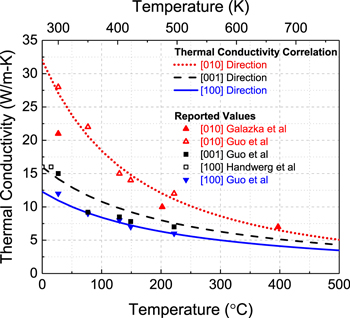
Figure 1. Temperature dependence of the thermal conductivity of β-Ga2O3 in different crystallographic directions.
Download figure:
Standard image High-resolution imageA potential early insertion point for Ga2O3 devices is for vertical geometry Schottky rectifiers, based on the availability of both thick epitaxial layers and conducting substrates.30–33 To achieve high reverse blocking capability in Ga2O3 rectifiers, a low doped n-type epitaxial layer is required, which leads to lower electrical conductance and in turn exacerbates heat generation in the epitaxial layer. Under deliberately induced failure at high current forward bias conditions, cracks may appear on the Schottky contact and delamination along the [010] crystal orientation has been observed.31,32 The failure mechanism has been mainly ascribed to plastic deformation of the lattice structure during device self-heating. Previous thermal simulations have shown that the main mechanism of heat generation in a vertical β-Ga2O3 Schottky device is Joule heating, and the highest temperature was observed near the metal-epi interface.34 Therefore, optimized thermal management has become a key consideration for advancement in device performance and mitigation of potential device failure under high-power operation conditions.1
We have previously shown that over a broad range of Schottky contact size (40–800 μm diameter), the devices fail at similar temperatures (270 °C–350 °C), independent of area, but that the current density at which failure occurs under forward bias is a strong function of contact size.31 For example, small devices (40 μm diameter) were able to achieve a forward current density of ∼2200 A.cm−2 before failure, while large devices (800 μm diameter) failed at < 200 A.cm2. The anisotropic thermal conductivity suggests that contact orientation may also play a role in determining the forward bias failure conditions.31
In this paper, we report on the orientation dependence of the Schottky contact on Ga2O3 rectifiers on the maximum achievable forward currents and the forward voltage threshold for the onset of thermally-induced damage. The use of asymmetric Schottky contacts with their long axis perpendicular to the [010] crystallographic direction is the optimum choice to maximize forward currents. This is a part of an effort to better understand thermal gradients in rectifiers to better understand device performance and to link these to fundamental failure and reliability mechanisms.
Experimental
The fabrication sequence for the Schottky rectifiers has been described previously,30–33 but in brief, begins with a layer structure of 10 μm Si-doped (3.5 × 1016 cm−3) epitaxial layer grown by Halide Vapor Epitaxy (HVPE) on (001) orientated 650 μm β-phase Sn-doped (n = 3.6 × 1018 cm−3) Ga2O3 substrate (Novel Crystal Technology). A full area backside Ohmic contact (20 nm/80 nm Ti/Au) was deposited by electron beam (e-beam) evaporation and annealed for 30 s at 550 °C in N2 using an SSI SOLARIS 150 rapid thermal annealer. To form a field plate, 40 nm Al2O3 and 360 nm SiNx dielectric were deposited using Cambridge-Nano-Fiji Atomic Layer Deposition and Plasma-Therm Plasma Enhanced Chemical Vapor Deposition tools, respectively. Windows with different geometries (0.25 × 0.5 mm2 rectangles with the long axis oriented perpendicular to either the [100] or [010] crystallographic directions or 0.354 × 0.354 mm2 squares of the same area) were opened using 1:10 diluted Buffered Oxide Etchant (BOE). Figure 2 shows images of the different contact orientations and shapes. The purpose of having these different Schottky contact geometries was to test the orientation dependence of forward bias current and resistance to damage under forward biasing stressing. The sample surface was then treated in O3 for 20 min to remove hydrocarbon and other contamination species. 400 μm Ni/Au (80 nm/320 nm) Schottky metal was subsequently deposited using E-beam evaporation with standard acetone lift-off.
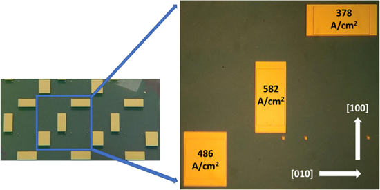
Figure 2. Optical microscope images of 0.25 × 0.5 mm2 rectangular Schottky rectifiers oriented with their long axis perpendicular to either [100] or [010] orientations and a standard square geometry rectifier of the same area. The maximum current density achievable with each orientation is also shown.
Download figure:
Standard image High-resolution imageThe rectifier forward and reverse current-voltage (I-V) characteristics were recorded on a Tektronix 370-A curve tracer. For forward bias stressing of the rectifiers, an Agilent Technologies 8114A pulse generator was used to apply continuous voltage bias at 95% duty cycle for 1 min at various voltage levels up to the point of device failure. The forward voltage was increased gradually by 1 V until a sudden irreversible increase of the reverse bias leakage current and irreversible decrease of breakdown occurred at a given reverse bias voltage. The forward currents were corrected for the probe resistance of 1.34Ω. Thermal images of the sample were taken using an Optris PI640 infrared camera. Some in situ Transmission Electron Microscopy images of devices operated to the failure point were taken using electron transparent functional specimens from the fabricated bulk β-Ga2O3 Schottky diode using focused ion beam (FIB).41–43 Electrical characterization was performed inside a field emission 200 kV FEI Talos F200X TEM equipped with energy dispersive spectroscopy (EDS) with 1.2 Å resolution.
For thermal simulations, a 3-D finite element analysis was employed to calculate the temperature distribution. The details of this steady state energy balance approach have been given previously. The steady state temperature contours of the rectifiers with various geometries were simulated at the maximum forward bias measured experimentally. The highest junction temperature at the center of the metal contact was used to compare the temperature rises of the different contact geometries and orientations.
Results and Discussion
Figure 3 shows forward I-V characteristics up to the failure point for rectifiers with either rectangular shaped contacts oriented in the two different directions, or the square contacts. Note that the absolute forward currents reached range from 0.48 A to 0.74 A, corresponding to current densities of 384–592 A cm−2 current density. Orienting the rectangular shaped contacts with the long side perpendicular to the [010] crystallographic direction in the Ga2O3 produces the largest current by ∼0.14 A relative to the square shape, while placing the long side perpendicular to [100] produces a similar penalty of 0.13 A relative to the square control contact. This is a clear demonstration of the need to take account of the anisotropic thermal properties of Ga2O3.

Figure 3. Forward I-V characteristics from the rectangular rectifiers oriented in the two different crystallographic directions and also the control (square) rectifier of the same area.
Download figure:
Standard image High-resolution imageFigure 4 shows the leakage current at −100V reverse bias for the three different geometry rectifiers as a function of the forward bias to which the devices were subjected. The three devices show a clear difference in the forward bias at which the onset of degradation, as measured by the sudden and concurrent increase in reverse current, is observed. The use of asymmetric Schottky contacts oriented in the correct direction can increase the threshold at which device degradation occurs by taking advantage of the higher thermal conductivity in the [010] direction. Figure 5 shows the full spectrum of device reverse leakage current vs voltage bias, where the device breakdown was defined as 3 mA cm−2. A breakdown voltage of ∼570 V was reported in this work, which is consistent with previously reported 10 μm epi device.
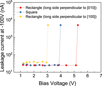
Figure 4. Reverse leakage current at −100V reverse bias for the different oriented rectangular rectifiers and the square rectifier, as a function of the forward bias at failure.
Download figure:
Standard image High-resolution image
Figure 5. Device leakage current and current density as a function of reverse voltage bias.
Download figure:
Standard image High-resolution imageThe rectifiers that failed consistently showed delamination of the epitaxial layer. There were also multiple crack lines observed along the [010] direction. Figure 6 shows a scanning electron microscope (SEM) image of a after forward biasing to failure. Note the oriented cracks that appear on the epitaxial layer surface-these eventually lead to complete delamination of this layer along the [101] crystallographic direction.31,32 Previous ultra-fast laser irradiation experiments44 showed that the inability to dissipate the heat in Ga2O3 produces mechanical failure of the material along natural cleavage planes. The concentration of heat in the lightly doped epitaxial layer relative to the heavily doped substrate leads to differential thermal expansion and delamination of the epitaxial layer. Raman mapping of Ga2O3 Schottky rectifiers confirms the concentrated heat generation near the metal/Ga2O3 interface.45 We have observed this for many samples, from different wafers and different contact sizes and orientations.
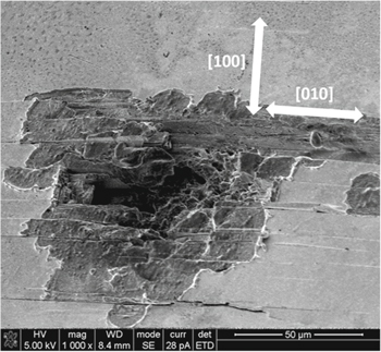
Figure 6. SEM micrograph of rectifier after forward biasing to failure.
Download figure:
Standard image High-resolution imageThe in situ TEM was also instructive. Figure 7 shows I-V's and TEM cross-sectional images of the symmetric contact rectifiers before and after failure. These rectifiers were formed into a TEM coupon by focused ion beam milling and thus one cannot compare the I-V's to the thin film devices. The current densities are shown on both log and linear scales at the top left and bottom right corner of the figure to amplify the differences, while TEM bright field images are shown for the total forward current through the electron transparent foil. There are defect clusters created near the top and bottom electrodes, which occur prior to the cracking and delamination. The elemental compositions in these clusters derived from the EDS data is shown in Fig. 8. There is a gold (Au) ball formed on the top surface as the cathode degrades, as well as Ga-rich and Au-Si-rich droplets formed within the Si-doped Ga2O3 epitaxial layer. These are stable to the point where the cracking and delamination leads to complete failure of the device. It will be interesting to see if the asymmetric contact design delays the creation of these droplets relative to the symmetric contact design.

Figure 7. In situ TEM micrographs of rectifiers before and after failure under forward bias conditions. The corresponding I-Vs and current densities are also shown for each condition.
Download figure:
Standard image High-resolution image
Figure 8. TEM and EDS data to identify the chemical composition in the observed defect clusters produced in the symmetric contact rectifiers by forward biasing. The Schottky contact is at the top of each image, while the bottom is the Ohmic contact.
Download figure:
Standard image High-resolution imageFigure 9 shows the steady state thermal simulation temperature profiles on the epi surface for the three different contact geometries, with the rectifiers biased at the corresponding failure condition. The anisotropic thermal conductivity leads to oval-shaped temperature patterns adjacent to the contact the thermal pictures for all three geometries, but a lower maximum temperature for the rectangular contact oriented perpendicular to [010]. The simulations assumed constant current density over the entire contact area, but the spreading resistance on the metal contact could lead to current crowding during experimental measurements with a probe.31 The experimental profiles recorded on the thermal camera under different contrast conditions are shown in Fig. 10. These were obtained at a current density of ∼120 A cm−2. We observe a circular temperature profile for the optimized oriented rectangular contact, oval for the square device, and a strong oval pattern for the rectangular device oriented with the long side perpendicular to [100]. For diodes with the same surface but only with different orientation, it is clear that the [100] direction greatly facilitate the dissipation of heat and enables a more spread-out thermal profile for diode with long edge perpendicular to this direction, and therefore a higher surface area for lateral thermal dissipation through the bottom heat sink. The impact of the anisotropic thermal conductivity is very pronounced in terms of the temperature profile generated.
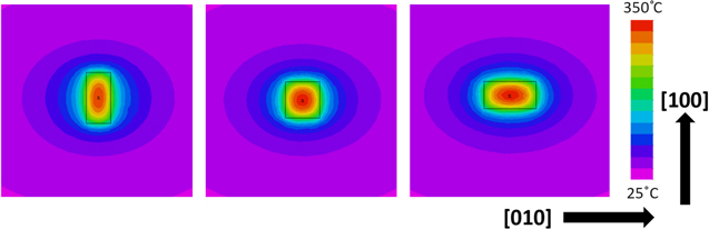
Figure 9. Simulated temperature distributions for different geometry rectifiers at their maximum forward bias.
Download figure:
Standard image High-resolution image
Figure 10. Thermal images of different geometry rectifiers at their maximum forward bias.
Download figure:
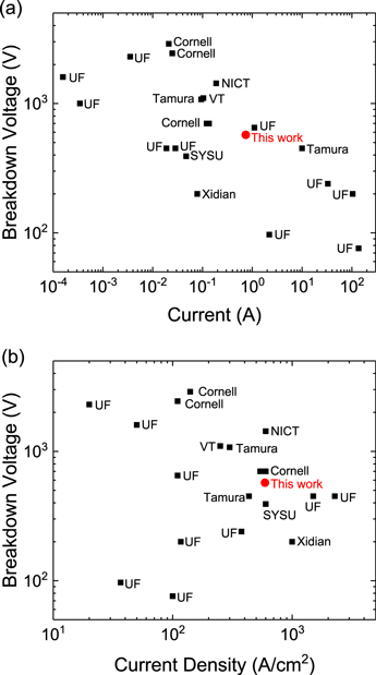
Standard image High-resolution imageFigure 11 shows the current performance for the state-of-the-art Ga2O3 vertical Schottky diodes in terms of breakdown voltage vs the maximum measured current Fig. 11a and current density Fig. 11b. A strong negative correlation can be found between the diode current and their respective breakdown voltage. The optimized diode design is inline with the published datapoints, and with the improvement of material growth, the breakdown voltage is expected to continue to improve for larger sized diode.17,30–33,46–58
Figure 11. Comparison of diode breakdown voltage vs device maximum measured current (a) and current density (b).
Download figure:
Standard image High-resolution image
Conclusions
The current state-of-the-art β-Ga2O3 vertical Schottky rectifiers are now reaching forward currents where thermal-induced failure can occur due to plastic crystallographic deformation near the epi-substrate interface. The thermal interfaces between the epitaxial drift layer and the underlying substrate is a bottleneck for heat dissipation. With an Arrhenius relationship between device mean time to failure (MTTF) and operating temperature, small changes in the device temperature can result in orders of magnitude differences in lifetime.38 The low and anisotropic thermal conductivity means that thermal management approaches are critical for Ga2O3. Direct evidence for this has been captured using an IR camera. One possible method that will form part of a larger scheme to address this is the fabrication of asymmetrical contacts along the higher thermal conductivity directions. It should be emphasized that in addition to device-level approaches, there is also a need for a holistic approach in which novel packaging materials, integration methods, and thermal management techniques that include transport across complex multi-material interfaces at the package and system levels are essential to produce Schottky rectifiers operating at realistic current levels.1,34–37,39,45,59 The traditional method of cooling electronic devices via heat spreading through thermal interface materials and high conductivity heat spreaders is likely insufficient for the applications envisaged for Ga2O3.60
Acknowledgments
The project was sponsored by the Department of the Defense, Defense Threat Reduction Agency, HDTRA1-17-1-011, monitored by Jacob Calkins and also by NSF DMR 1856662 (Tania Paskova). Research at NRL was supported by the Office of Naval Research, partially under Award Number N00014-15-1-2392. The content of the information does not necessarily reflect the position or the policy of the federal government, and no official endorsement should be inferred.