
Abstract
The demand for ultrasensitive and reliable sensors for biomolecules detection and disease diagnostics has increased in modern-day scientific research. Semiconductor nanowire field-effect transistors (FET) can be used as biochemical sensors for ultrasensitive, selective, and label-free detection of low ion concentrations, molecules, proteins, DNA, and viruses. Thus, most devices with back gates for these nanowires are limited to large-scale fabrication and integration. In this study, a novel side-gated silicon nanowire (SiNW) FET was fabricated using complementary metal oxide semiconductor compatible technology. The side-gated SiNW-FET was employed as a biosensor for ultrasensitive detection of BRAFV599E gene mutation. Specific electrical performance was observed when the nanowire surface was functionalized using complementary and 1-base mismatch target DNA. A nanowire-based sensor was used to distinguish between the complementary and 1-base mismatch DNA through the dehybridization process at different melting temperatures. Results demonstrated that the side-gated SiNW-FET device could act as a label-free, highly sensitive, and selective biosensor for gene mutation sensing. Our approach offers the possibility of multidetection of the biological species with local control elements in a single integrated circuit.
Export citation and abstract BibTeX RIS

This is an open access article distributed under the terms of the Creative Commons Attribution 4.0 License (CC BY, http://creativecommons.org/licenses/by/4.0/), which permits unrestricted reuse of the work in any medium, provided the original work is properly cited.
Ultrasensitive and selective biochemical sensors have been widely developed and used in the fields of biomedical diagnostics, drug discovery, genomics, and proteomics.1,2 Recent research have shown tremendous advancements in the use of nanomaterials configured as field-effect transistors (FET) for biomolecule analysis. Silicon nanowires (SiNW) have been reported as one of the most promising platforms for label-free, real-time, and ultrasensitive electrical detection of proteins and many other biological species. Ultrasensitive biological and chemical species are significant and fundamental targets for early detection and screening of diseases, viruses, and flu because of their small size and large surface-to-volume ratio.3–6 This enables local charge carriers to cause a change in current due to the electric field when the analytical molecules bind to specific recognition molecules at the nanowires surface.7 This effect is strong for the charges at the surface of a nanowire to be sensed because of depletion or accumulation of charge carriers, which affects the conduction pathway of nanowires.8,9 Several approaches and structures have been proposed to achieve this effect; among them, one-dimensional nanostructures have demonstrated to be an excellent candidate for ultrasensitive, miniaturized molecule sensors. Semiconductor-nanostructure-based sensors such as single-wall carbon nanotubes,10 silicon nanowires,6 SnO2 nanowires,11 and In2O3 nanowires12 can be used to detect changes in surface charge in the presence or absence of molecular species in the nanostructure. Furthermore, the high surface-to-volume ratio of nanostructures and their conductance as the sensitivity may be sufficient for the detection of a single molecule.
Recent studies based on "bottom-up" nanostructures have been limited by complex integration, which requires transferring and positioning of the nanostructure for a reliable sensor property.13,14 In this study, a standard "top-down" semiconductor15,16 process was employed to fabricate SiNWs to address these issues, and the SiNWs were used as a biosensor for the screening of DNA molecules based on their intrinsic charge.17,18 The fabrication approach employed creates high-density and high-quality nanoscale sensors that can be incorporated into silicon-based signal processing and communication circuits.
Global "back-gate" structures have been commonly used to obtain working SiNW-FETs.19 In such structures, all devices on the wafer are applied to the same gate voltage and cannot be controlled individually. This allows the "back gate" to cover the entire source/drain (S/D) region,19–21 inducing large parasitic capacitance due to the gate and S/D metal electrodes. Therefore, these problems can be solved by using the proposed "top-gate" and local "back-gate" configurations. However, "top-gate" designs lack a contact area with the biomolecules, and local back gates remain limited because of the difficulty of their large-scale integration.22
This study addressed the aforementioned problems of SiNW-FETs using an in situ local oxidation of silicon (LOCOS) isolation process to propose and demonstrate a side-gated SiNW-FET configuration.23 By patterning a doped silicon-on-insulator (SOI) film to form local gates, a selected gate for each specified SiNW-FET can be realized.
The LOCOS process helps to obtain a higher surface-to-volume ratio in shrinking the nanowire.5,24 Thus, the detection sensitivity of LOCOS-produced devices is high because the signal transduces efficiently due to the sizeable surface-to-volume ratio. The side-gated SiNW-FETs fabricated using SOI wafers in this study provide an individual gate for each device and hence exhibit low current leakage and excellent field effect properties. Thus, these FETs will be easily integrated into integrated circuits (ICs) for the development of multidetection systems in the future.
False positive error and sensitivity are important factors in the application of SiNW-FET biosensors. False positive errors reduce the reliability of a biosensor system. Therefore, we determined whether fully complementary and one-mismatch DNA sequences could be distinguished using our device. The ability of the fabricated side-gated SiNW-FET as a label-free biosensor was evaluated through detection of the BRAFV599E gene mutation. A BRAF gene mutation causes cancer in humans, most notably melanomas, as well as the most common aberration discovered in sporadic papillary thyroid carcinomas (PTCs).25,26 Increased basal kinase activity and decreased oncogenic stimulation were observed in individuals with BRAFV599E gene mutations.26 Therefore, excellent background analysis is required to characterize BRAFV599E gene mutations at the molecular level for early tumor detection.
Materials and Methods
Fabrication of side-gated SiNW-FET
A "top-down" CMOS wafer microfabrication technique was employed to produce the side-gated SiNW-FET; this technique has advantages such as high consistency and suitability for ICs and large-scale production. Figure 1. illustrates the proposed technique and procedures for device fabrication. First, standard RCA cleaning was performed on a silicon wafer. A 6-inch (100) commercially available SOI wafer was used, which required definition of the lateral active layer (in-plane, two-dimensional) to determine its nanoscale dimensions necessary for the nanowire-type device. The sensitivity of the sensor is strongly affected by the size of SiNW. Consequently, SOI wafers with 50 and 150 nm thick intrinsic silicon and buried oxide, respectively, were selected as the device substrate (Fig. 1a). Fig. 1b shows the formation of a shrinking nanowire through the LOCOS process. The fabrication process employed was based on our previously reported methods.24,27 Stacked films of silicon oxide and silicon nitride were deposited sequentially to serve as the masking layer. Optical lithography and plasma etching were used to define the active region, followed by an oxidation process to oxidize the exposed silicon. The underlying silicon film was then shrunk to form a nanowire as well as the source, drain, and side gate. After removing the silicon oxide and silicon nitride films, ion implantation was performed using 20 keV and a dosage of 5 × 1015 cm−2 through an arsenic ion beam (As+) on the source, drain, and side-gate areas. Thereafter, rapid thermal annealing was performed at 1050°C for 30 s in a nitrogen atmosphere (Fig. 1c). A tetraethyl orthosilicate oxide film was formed as the passivation layer, and the contact pad regions at the source, drain, and gate areas were opened. A metal film formed using a physical vapor deposition sputter system was deposited as the electrode through a lift-off process (Fig. 1d). In the final stages of the fabrication, the detection area was etched back to expose the silicon nanowires (Fig. 1e). Prior to immobilization, all the devices were preserved in a clean room for at least 1 week to ensure thickness saturation of the native oxide.
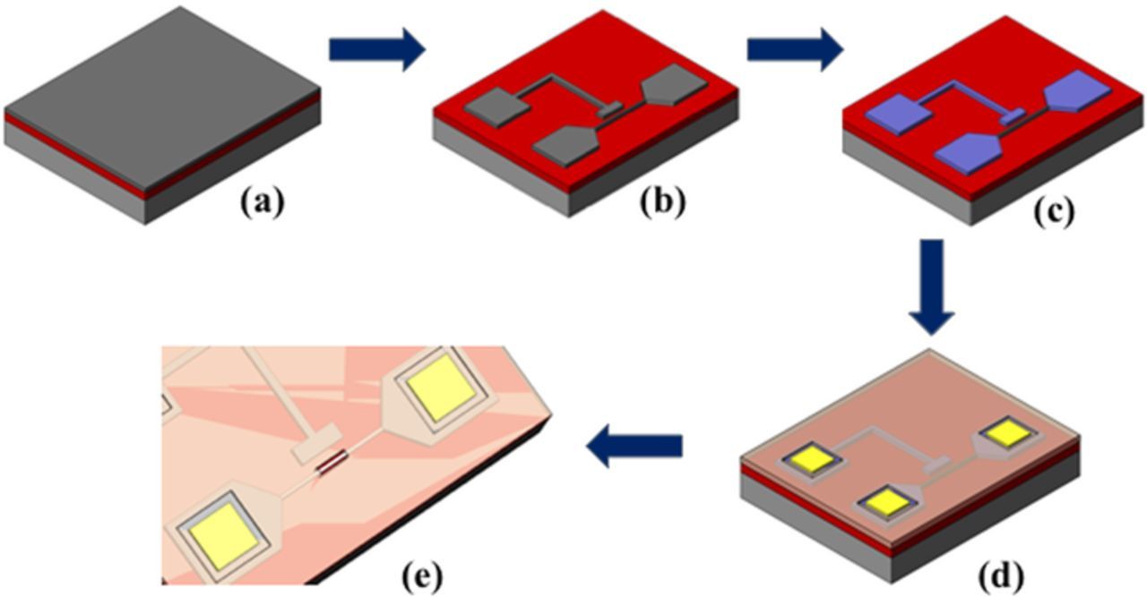
Figure 1. Flowchart of the side-gated SiNW-FET device fabrication process on an SOI wafer. (a) The 6-inch SOI wafer (50-nm intrinsic Si; 150-nm buried oxide) employed as the substrate. (b) Patterning using photolithography and dry etching systems. (c) Source/drain implantation and annealing. (d) Contact pad deposition at the source/drain. (e) Formation of a passivation layer, followed by etching back the detection region for DNA immobilization (red circle).
Covalent attachment of capture DNA to the nanowire
Chemical modification of the SiNW surfaces was necessary because it allowed and enhanced binding of the biological probe molecules. Therefore, prior to immobilization and sensing, the device was thoroughly cleaned using the standard cleaning process and protocol to avoid contamination. The nanowire surface was modified to enable DNA attachment for biosensing. Therefore, the nanowire surface was modified using the amino group APTES (3-amino-propyl-triethoxy-silane). Samples were prepared based on the following three primary processes, as illustrated in Fig. 2.
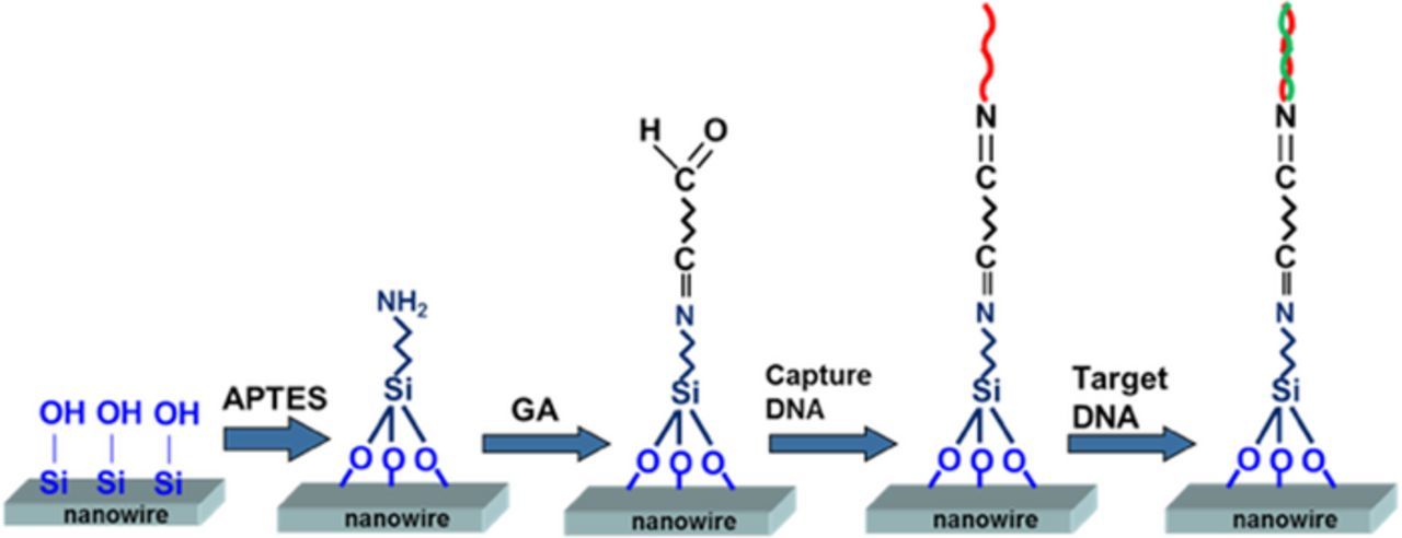
Figure 2. Self-assembly processes for immobilization of the capture DNA and hybridization of the target DNA. (I) SiNW presents a native oxide on its surface coated with APTES. (II) Glutaraldehyde linkage to amino groups. (III) Terminal 3-amino groups of the capture DNA strands react with the aldehyde groups. (IV) Complementary target DNA is hybridized to the capture DNA on the SiNW surface.
Surface immobilization
First, the SiNW-FET was cleaned using acetone and ethanol for 30 min, rinsed with deionized (DI) water, and then dried clean using nitrogen (N2) purge. The devices were carefully handled to avoid contamination through touching of the SiNW surfaces after cleaning. Thereafter, the samples were immersed in 10% APTES in aqueous solution for 30 min at 37°C. Then, the samples were rinsed with DI water and dry heat at 120°C for 10 min. After heating, the SiNWs were immersed in a linker solution of 2.5% glutaraldehyde for 30 min at room temperature, followed by rinsing with phosphate-buffered saline (PBS; 120 mM NaCl, 2.7 mM KCl, and 10 mM phosphate buffer; pH 7.4; Sigma–Aldrich) solution and drying using an N2 purge.
Single strand DNA (ssDNA) immobilization
Covalent immobilization was performed to bind the terminal 3'-amine group of the oligonucleotides to carbonyl groups on the SiNW surfaces. One drop (100 μL) of a prepared solution containing 1 μM ssDNA named capture DNA (Blossom Biotechnologies, Taipei, Taiwan) was placed in the detection region for 1 h to ensure DNA immobilization on the SiNWs. Unreacted carbonyl groups were blocked using ethanolamine (Sigma–Aldrich). Immediately after immobilization, DI water was used to wash the SiNW surfaces, which were then dried using N2.
Complementary and noncomplementary ssDNA detection
After the functionalization of the immobilized capture DNA, probe binding was performed as described in Surface immobilization and Single strand DNA (ssDNA) immobilization sections. Another ssDNA named target DNA, which is complementary to capture DNA was applied to hybridize with the capture DNA. To examine the detection ability of the SiNW-FET device, the target DNA was diluted to various concentrations with PBS buffer solution. The target DNA was injected into the microfluidic channel. After that, the channel was washed with PBS to remove the excess target DNA and purged through N2 drying. The mismatched target DNA strands were used to demonstrate the detection ability of the sensor.
Electrical measurement of SiNW-FET devices for detecting target DNA
The electrical properties of the immobilized DNA sensors were characterized using a semiconductor parameter analyzer (Agilent 4156A). The IDS–VGS curves were analyzed in each step to ensure surface modification and immobilization were done efficiently. The IDS–VGS curves of the SiNW-FET devices were recorded when the complementary target DNA was injected into the detection area; hybridization was performed to capture the DNA. The specific detection ability of the SiNW-FET was examined through mismatch DNA strands by comparing its electrical properties.
Results and Discussion
In the LOCOS method, lateral oxidation is a key process and affects the narrowing of the nanowires, causing a certain degree of deviation from the original design. Fig. 3a shows a schematic of the nanowire shrinkage process using lateral oxidation. Atomic force microscopy images of the gate and nanowire are shown in Fig. 3b. The rise in morphology indicated in the figure can be attributed to the silicon-oxide film formed by the LOCOS process. Fig. 3c presents scanning electron microscopy (SEM) images of the fabricated side-gated SiNW-FET. The length of the nanowire in our design was 12 μm. The nanowire width was estimated to be 120 nm.

Figure 3. (a) Schematic of the LOCOS process used to narrow the nanowire. (b) Atomic force microscopy image of the gate and nanowire of the SiNW-FET device. SEM images of a 120-nm side-gated SiNW: (c) top view and (d) amplification of the area.
A MOSFET gate was used to control the energy barrier and Ion/Ioff state. Figure 4a shows the dependence of drain current (IDS) and square root of drain current (IDS1/2) on gate voltage (VGS) at drain voltages (VDS) of 1.0 V, and the plots of IDS versus VDS for various VGS are shown in Fig. 4b. In Fig. 4a, IDS1/2 vs VGS is linear, and the x-intercept of this straight line is mathematically defined as the threshold voltage (Vth).28 Therefore, the threshold voltage is estimated to be −0.5 V from Fig. 4a. The Vth of an n-channel MOSFET (nMOSFET) can be defined as the VGS that results in the electron concentration in an inverted n-type channel is the same of hole concentration in the transistor substrate. When a voltage is applied to the gate, the electric field induced the electrons in the nearest substrate to become highly concentrated in that region. Thus, when the VGS is less than the Vth, the transistor is turned off, and no current passes from the drain to source. If the VGS is higher than the Vth, the transistor turns on because of the accumulation of more electrons than holes near the substrate gate. Therefore, the channel should be subjected to strong inversion to create more current flow from the drain to the source region.
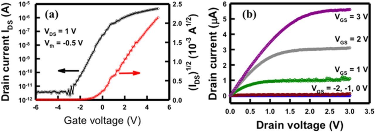
Figure 4. Electrical properties of side-gated SiNW-FET. (a) the dependence of drain current (IDS) and square root of drain current (IDS1/2) on gate voltage (VGS) at drain voltages (VDS) of 1.0 V; (b) IDS–VDS characteristics of the device for VGS was from −2 to 3 V.
The fabricated side-gate SiNW-FET was an n-channel FET device; the electron carriers passing through the SiNW-FET from the source to drain could be efficiently modulated by biasing the side-gate voltage. For example, the channel electron barrier was enhanced and the drain current was decreased when a negative voltage was applied to the gate, whereas the drain current was increased when a positive voltage was applied.5
The attachment of positively or negatively charged molecules to the nanowire surface resulted in additional charges in the channel, thereby altering the detected current. If an electrically charged molecule is adsorbed onto the nanowire surface, an electric field was then created, which either accumulates or depletes electrons within the channel surface. However, this depends on the bonded charge molecule and charge carriers of the same or opposite charge. DNA is suggested to be negatively charged,18 therefore, when the DNA becomes bound to the nanowire, a right-shifted IDS–VGS curve is obtained; that is, a high VGS can be applied to prompt the inversion layer to shift the Vth positively. Thus, we can measure the Vth shift to ensure binding of the target DNA and the capture of the DNA for detection.
In this study, a fragment of BRAFV599E gene mutation was selected as the target DNA. Through the use of the charge effect, the SiNW-FET device was used as a biosensor to detect biochemical molecules. A 30-mer DNA strand of the sequence 5'-AAATATATTA-TTACTCTTGA-GGTCTCTGTG-3' was used as the capture DNA. This capture DNA sequence was fully complementary to that of the BRAFV599E gene mutation. Typically, DNA has a double-stranded helix structure. The complementary base pairs of double-stranded DNA (dsDNA) are linked by hydrogen bonds, guanine (G) links to cytosine (C), and adenine (A) links to thymine (T). Therefore, the BRAFV599E gene mutation was designed to the specific gene sequence 3'-TTTATATAAT-AATGAGAACT-CCAGAGACAC-5'. Fig. 5a illustrates the ability of the SiNW-FET biosensor to detect cancer-related BRAFV599E gene mutation. The Vth of the device by the capture DNA modified, measured in PBS buffer solution, was −0.5 V (baseline). Various concentrations of the target DNA were assessed. The BRAFV599E gene mutation adsorbed onto the surface of the sensor. The results revealed a further shift of the IDS–VGS curve to a higher voltage as the target DNA concentration was increased. The curves shifted to higher voltage because the DNA had negative charge and hybridization of the target DNA to the capture DNA induced more negative charge on the nanowire surface, most likely a negative gate voltage applied to the SiNW-FET device.29 Therefore, the shift to higher voltage of the IDS–VGS curve indicates successful hybridization of the complementary gene mutation with the capture DNA. The IDS1/2 vs VGS plot is shown in the inset of Fig. 5a. It is noted that the gate of the SiNW-FET device was buried under an oxide film, the gate did not directly contact to the buffer solution. This structure provides a stable sensing property because the gate leakage is very small.30,31

Figure 5. Concentration-dependent electrical response of the capture-DNA-modified SiNW-FET sensor in detecting the target DNA. The IDS–VGS curve of the baseline was obtained in PBS buffer (black line); PBS buffer solutions containing target DNA at various concentrations (10 fM, 1 pM, 100 pM, 10 nM) were injected, respectively, and IDS–VGS curves were recorded. Inset is the IDS1/2 –VGS plot of FET sesnor. (b) Voltage shift (from n = 4) of the SiNW-FET sensor plotted with respect to the target DNA concentration. The voltage shift was extracted from (a) at a constant drain current (IDS = 1 nA).
The relationship between capture DNA concentration and the voltage shift of the SiNW-FET biosensor is illustrated in Fig. 5b. The relationship between voltage shift and the logarithm of target DNA concentration (10 fM, 1 pM, 100 pM, and 10 nM) is highly dependent and linear. As reported by Nair and Alam,32 the relationship between the biosensor response and DNA concentration can be given as follows:
![Equation ([1])](https://content.cld.iop.org/journals/1945-7111/165/13/B576/revision1/d0001.gif)
Where S(t) is the sensor's response to either a voltage or current shift and [ρ0] is the DNA concentration. Our detection results are in agreement with this equation, which indicates that the response of the SiNW-FET biosensor exhibited a logarithmic dependence on the DNA concentration. The linear fit of the calibration curve of the SiNW-FET can be expressed as
![Equation ([2])](https://content.cld.iop.org/journals/1945-7111/165/13/B576/revision1/d0002.gif)
For a detected concentration range of 10 fM–10 nM, the correlation coefficient was 0.981. The detection limit of the fabricated SiNW-FET biosensor was estimated to be 0.83 fM. The detection limit was obtained from the minimal DNA concentration, which yielded a voltage shift that is three times the standard deviation.
The specific detection ability of the target DNA is a critical factor for the biosensor. Determining the thermal stability of nucleic acid is one of the methods used to evaluate whether DNA is fully complementary or mismatched. DNA is typically a double-stranded structure at room temperature. When the temperature is increased, hydrogen bonds within DNA are broken, the double strand melts, and a single-stranded structure is formed. Melting temperature (Tm) is an index of the thermal stability of dsDNA, which is dependent on the DNA sequence, base number, concentration, solvent condition, and mismatch structure.33,34 For fully complementary dsDNA strands, the binding strength is larger than that of mismatched dsDNA; thus, the melting temperature of complementary dsDNA is higher than that of mismatched DNA.
ssDNA exhibits a UV absorption peak at a wavelength of 260 nm because of its aromatic ring structure. When the temperature is increased, dsDNA melts, and thus, its UV absorbance increases. Therefore, the melting level of DNA strands can be determined by measuring their UV absorption. Fig. 6 illustrates the absorbance of the fully complementary target dsDNA at various temperatures. Initially, the temperature was retained at 23°C, and the absorbance value was low. When the temperature was increased up to 72°C, the absorbance increased sharply, indicating dsDNA denaturation. When the sample was cooled, the ssDNA rehybridized into dsDNA, and thus, the absorbance gradually decreased to its initial level.

Figure 6. UV absorbance response of the fully complementary target dsDNA at various temperatures.
Fig. 7 shows the electrical responses of the SiNW-FET biosensor in detecting the complementary and 1-base mismatched DNA strands. For the complementary target DNA detection illustrated in Fig. 7a, when the capture DNA first became attached to the nanowire surface, Vth shifted toward a higher voltage. Next, the 10 nM complementary target DNA was employed to hybridize the capture DNA, which resulted in a further positive shift of Vth. This explains the result of high negative charge on the nanowire. In this study, denaturation was performed. The hybridized target DNA was first washed with DI water at 60°C, and the electrical response was measured. As shown in Fig. 7a, the I–V curve after DI water washing at 60°C was unchanged, implying that the target DNA was fully complementary to the capture DNA. When the sensors were washed with DI water at 72°C, the nanowire device was restored to its near-original Vth once the only capture DNA attachment was complete. The electrical response of the SiNW-FET device after DI water washing 72°C indicates the occurrence of denaturation; that is, the complementary target DNA separated from the capture DNA and was stripped off through washing. The detection process shown in Fig. 7a demonstrates that DI water washing at 72°C efficiently dehybridized the complementary target DNA from the probe DNA, which was consistent with the UV absorption results presented in Fig. 6.

Figure 7. Electrical response of the capture-DNA-modified SiNW-FET sensor in detecting complementary and mismatched target DNA. (a) IDS–VGS curve of complementary DNA detection; (b) IDS–VGS curve of mismatched DNA detection; PBS buffer solution containing three-base-mismatched target DNA strands (10 nM) was injected and the IDS–VGS curves were recorded.
For comparison, noncomplementary DNA was also used as the target DNA of the SiNW-FET device. We designed a DNA sequence containing one mismatch compared with the probe DNA sequence, 3'-TTTATATAAT-AATGACAACT-CCAGAGACAC-5', and the electrical response is illustrated in Fig. 7b. When the mismatch target DNA hybridized to the capture DNA on the SiNW-FET device, a positive shift of the ID–VGS curve was also observed. However, when the mismatched DNA was washed using 60°C DI water, the ID–VGS curve shifted back to that of the capture DNA attachment only, indicating that the mismatch target DNA was stripped off by washing with 60°C DI water. Compared with the result obtained for complementary target DNA shown in Fig. 7a, the mismatched samples could be dehybridized using DI water as low as 60°C because of the lower melting temperature of the mismatched dsDNA sequence. Thus, both the complementary target DNA and mismatch DNA caused shifts in the biosensor's electrical properties. Although it cannot be confirmed that the ID–VGS current changes were caused by the target or mismatched DNA binding to the SiNW-FET,35 the melting temperatures of the complementary and mismatched DNA are different; therefore, we can identify complementary and mismatched DNA by washing with DI water of different temperatures. Figure 8 shows a comparison of the Vth shift of the SiNW-FET in detecting complementary and mismatch target DNA sequences. It can be seen that the difference between complementary and mismatch target DNA sequences after 60°C DI water washing.
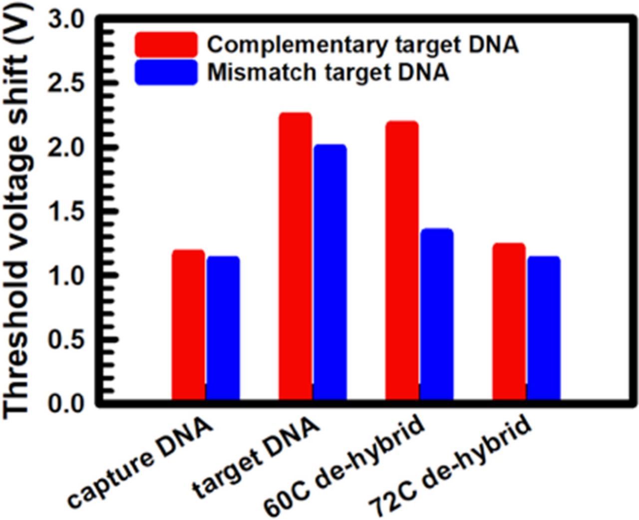
Figure 8. Comparison of threshold voltage shifts of the SiNW-FET sensors in detecting complementary and mismatched target DNA at capture DNA only, target DNA hybridized, 60°C DI water hybridization, and 72°C DI water hybridization.
Conclusions
We demonstrated a novel approach to the fabrication and immobilization of side-gated SiNW-FETs for detection of BRAFV599E gene mutation. Our fabrication technique showed crucial positive results by integrating "top-down" CMOS-FET compatible technology and the LOCOS isolation process. The fabricated device has lower current leakage and excellent field effect properties compared with on-air dielectrics; moreover, it is capable of being integrated into ICs. The IDS–VGS characteristic curve of the SiNW-FET exhibits approximately six orders of magnitude on Ion/Ioff, and the Vth positively shifted by 0.91 ± 0.03 V after hybridization of 10 nM concentrations of BRAFV599E gene mutation. These results, the different melting points (temperatures) in particular, demonstrate that the SiNW-FET detects favorably under different temperatures and is sensitive and selective for gene mutation sensing. Finally, we believe that this approach could help in the development of highly parallel detection techniques for multiple biochemical species on control elements in a single IC in the future.
Acknowledgments
This study is financially supported by the Ministry of Science and Technology, Taiwan, through grant number MOST106-3114-E-009-001. The authors would also like to thank the Nano Device Laboratories for their support in the fabrication process.
ORCID
Chi-Chang Wu 0000-0002-3013-8401