Abstract
This paper presents a switching circuit for high breakdown-voltage Ga2O3 vertical Schottky rectifiers. Field-plated edge-terminated (FPET) vertical Schottky diodes were fabricated on a 20-μm thick Si-doped n-type Ga2O3 drift layer which was grown on the 650-μm thick β-Ga2O3 substrate via halide vapor phase epitaxy (HVPE). The measured reverse recovery time of the proposed Ga2O3 Schottky diode was 81 ns when switched to a reverse bias voltage of −900 V. The implementation of a switching circuit with the novel Ga2O3 diode is the first demonstrated at such a high switching voltage. This paper also provides insights for the practical implementation of the Ga2O3 vertical Schottky rectifiers from device fabrication to circuit design.
Export citation and abstract BibTeX RIS

This is an open access article distributed under the terms of the Creative Commons Attribution 4.0 License (CC BY, http://creativecommons.org/licenses/by/4.0/), which permits unrestricted reuse of the work in any medium, provided the original work is properly cited.
With the increasing demands of switching power electronics, wide-bandgap materials such as silicon carbide (SiC), gallium nitride (GaN), and gallium oxide (Ga2O3) have attracted intensive research and development. Wide-bandgap materials can provide higher switching speeds, larger blocking voltages, lower on-resistance (losses), and higher operating temperature ranges than conventional silicon-based materials. Among various wide-bandgap materials, Ga2O3 has been considered a potential candidate for next-generation power electronics because of its ultra-wide bandgaps (Eg) of 5.3 eV (α-phase) and 4.9 eV (β-phase),1–3 which translate to around 5–9 MV/cm of a critical electric field. Compared with SiC and GaN, the larger bandgap and melt growth options with Ga2O3 offers the potential for higher breakdown fields, high Baliga's Figure of Merit (BFoM), and potentially lower costs in materials and fabrication processes.1–17 From both theoretical analysis and state-of-the-art prototype, Ga2O3 materials help to minimize the size of power devices while maintaining high operation efficiency in switching power electronics.
Since p-type doping, which would improve the breakdown voltage of devices with guard rings, has not yet been demonstrated for Ga2O3, the focus has been on field-plated vertical rectifiers to achieve high reverse blocking capability characteristics at high current density. A Schottky rectifier is an attractive unipolar high-power device, which is formed by Schottky non-linear contact on top of a drift region;17–19 it provides fast, soft switching characteristics to avoid unwanted electromagnetic interference (EMI) output.
Switching power devices have been implanted into different applications such as electric motor drivers, DC-DC, and AC/DC converters.18,20,21 A common approach is to use hybrid power converters consisting of Si MOSFETs and SiC rectifiers,22 Schottky rectifiers can provide high-power efficiency due to their fast switching speed, low switching power losses, and high-temperature operation capabilities.18 Moreover, vertical geometry Ga2O3 rectifiers have shown promise for future high-power devices and high-current switching capabilities. Yang et al.23 demonstrated that Ga2O3 vertical rectifiers could reach 2300 V of breakdown by using a thicker drift layer and lower carrier concentration with field plate design. Also, Ga2O3 diodes for high-current switching applications have been demonstrated.24–26 However, the switching capability of Ga2O3 vertical Schottky rectifiers has only been demonstrated at low reverse voltages (VR).23,25,27 There are limited studies on high-voltage switching of Ga2O3 Schottky diodes. Furthermore, the practical implementation of high-voltage Ga2O3 Schottky rectifier circuits still faces many challenges, such as high-current tolerance and speed constraints from stray board parasitics and the quality of driving signals.
Recently, promising progress in the development and fabrication of Ga2O3 materials and devices has shown the potential for practical applications. However, due to the limited numbers of prototypes in early development, device model and circuit analysis for realizing Ga2O3 power electronics is necessary. Some research works28 investigated the modeling of new Ga2O3 devices via computer-aided-design (CAD) tools, which helped to speed up device characterization and predicted developed device performance. With accurate parameter extraction and modeling, a circuit-intensive simulator can be used to build power electronic circuits for practical applications and performance improvement.
This paper presents the design flow for device modeling, circuit implementation, 900 V Ga2O3 device fabrication, and integration of a Ga2O3 rectifier. The first section describes how Ga2O3 vertical Schottky rectifiers were fabricated on a 20-μm drift layer with a high-voltage switching circuit at 900 V for nanosecond reverse-recovery time. The following section analyzes the design details of the circuit in order to accommodate the high reverse voltage and to enhance the switching speed. The final section presents the measurement results of the proposed circuit design techniques for the Ga2O3 vertical Schottky rectifiers.
Fabrication and Characterization of High-Reverse Voltage Ga2O3 Schottky Rectifiers
Field-plated, edge-terminated (FPET) vertical Schottky diodes were fabricated on a 20-μm thick Si-doped n-type Ga2O3 drift layer grown on a 650-μm thick β-Ga2O3 substrate using halide vapor phase epitaxy (HVPE).23–26 The epi layer growth for Ga2O3 is still developing, and the breakdown voltage of the vertical diode is heavily relating to the number of defects within the drift region. Besides, the breakdown would still occur on the edges of these device contacts. Therefore, a careful fabrication procedure is essential. The β-Ga2O3 substrate was an Sn-doped Ga2O3 single crystal wafer with (001) surface orientation grown by the edge-defined film-fed method with a carrier concentration of 3.6 × 1018 cm−3. A back side ohmic contact was formed with electron beam deposited Ti/Au followed by rapid thermal annealing at 550°C for 30 seconds in nitrogen (N2). Next, 40 nm of SiO2 and 360 nm of SiNx were deposited as dielectric layers. Dielectric contact windows were opened with buffered oxide etchant (BOE). E-beam evaporated Ni/Au (80/420 nm) metallization was used for the Schottky contacts, which overlapped the dielectric windows by 10 μm. Figure 1 shows a cross-sectional schematic and micrograph of the FPET rectifiers with a dielectric window opening of 400 μm × 400 μm.
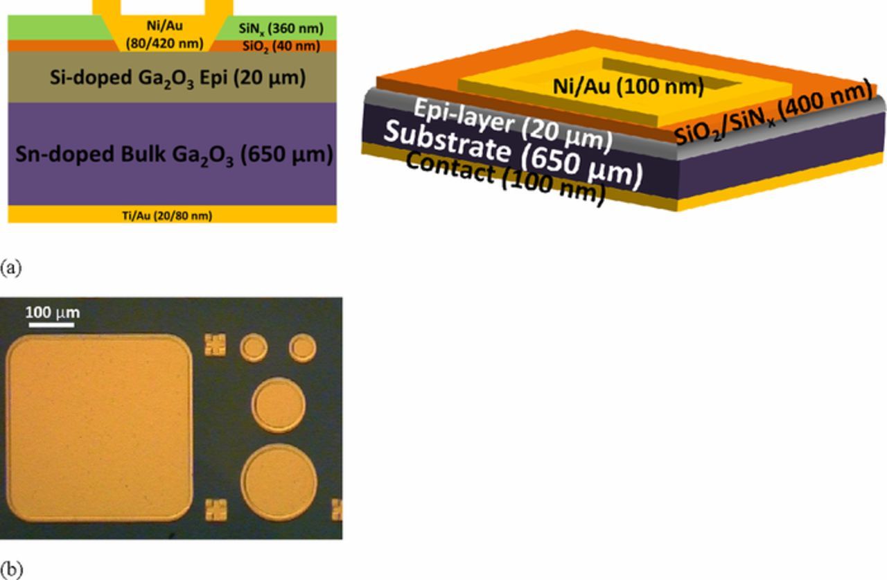
Figure 1. (a) Schematic of field-plated edge-terminated Ga2O3 vertical geometry Ni/Au Schottky rectifier structure with a 20-μm drift layer (b) micrograph of the fabricated Ga2O3 diode.
An Agilent 4156C was used to measure the diode DC characteristics up to the equipment's voltage and current limits of 100 V and 100 mA, respectively. Beyond these limits, a Tektronix 370A curve tracer was used to measure the reverse breakdown voltage. A current probe along with a Micsig (DP10013) differential probe were used to characterize the diode switching characteristics. Figure 2a shows the forward-biased diode characteristics that were measured from a 0–1.5 V bias voltage. The extrapolated Schottky barrier height (φb) and ideality factors were 1.05 eV and 1.03, respectively, consistent with reported values.14 The carrier concentration in the drift region was calculated from capacitance-voltage measurements to be 2.01 × 1015 cm−3. The diode on-state resistance was 18.2 mΩ-cm2, which yields a figure of merit (VB2/RON) value of 159 MW-cm−2. Figure 2b shows the diode reverse characteristics with a reverse breakdown voltage of 1711 V. This high breakdown voltage offers an opportunity for high-voltage power switching applications, such as AC-DC converters and automotive chargers.
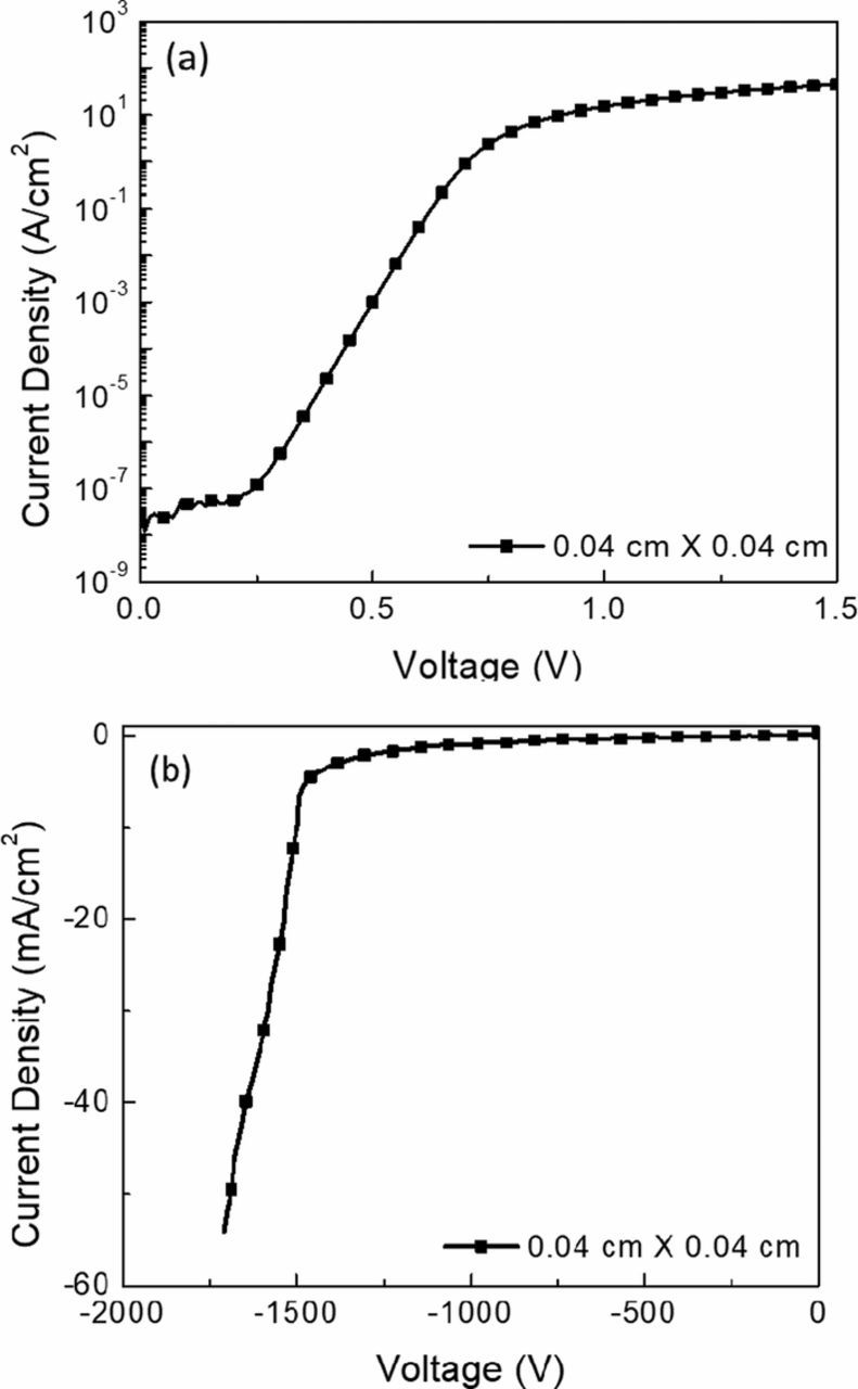
Figure 2. (a) Forward and (b) reverse current density-voltage characteristic for a Ga2O3 field-plated rectifier with a breakdown voltage of 1711 V for device size of 0.4 cm × 0.4 cm.
Modeling for High-Voltage Ga2O3 Vertical Schottky Rectifiers
Based on the current-voltage (I-V) characteristics, essential SPICE parameters of the fabricated Ga2O3 diode can be extracted for device modeling with a computer-aided design (CAD) tool. The forward I-V characteristics for these Schottky contacts on a moderately doped drift region were modeled using the thermionic emission model:
![Equation ([1])](https://content.cld.iop.org/journals/2162-8777/8/7/Q3229/revision1/d0001.gif)
where e is the electronic charge, k is Boltzmann's constant, n is the ideality factor, T is the temperature, and Is is the saturation current. The saturation current (Is) is given by
![Equation ([2])](https://content.cld.iop.org/journals/2162-8777/8/7/Q3229/revision1/d0002.gif)
where A is the Schottky contact area, A** is the Richardson constant, and φb is the Schottky barrier height. The effective Richardson constant for Ga2O3 has been reported in Ref. 29. In this study, a Richardson constant of 43.35 A.cm−2.k−2 was used for calculation of the Schottky barrier heights and ideality factors, and the extrapolation method for these calculations was described by Cheung et al.30
In addition to the static I-V response, dynamic switching characteristics are essential in the power rectifier design. A Ga2O3 diode takes a finite time to transit from the reverse bias (off state) to forward bias (on state) state and vice versa. This behavior is crucial for high-power systems since the power loss in the transitions is the significant loss of the switching behavior. A Ga2O3 Schottky diode has a minimal current overshoot during the switch from forward-biased conduction to the reverse blocking state because the reverse recovery time only depends on the capacitance, rather than on the minority carrier recombination. However, measuring fast response times at a high reverse voltage remains challenging. Therefore, due to the limitations of the available high-speed and high-voltage measurement instrument, a fast switching circuit was used to verify the Ga2O3 rectifier operation in high reverse voltage situations.
Circuit Implementation and Design Considerations for Fast-Switching Ga2O3 Diodes
Figure 3a shows the schematic of the rectifier circuit, which consists of an inductor (J.W. Miller 1140–153K-RC, 15 mH), a 900 V Ga2O3 rectifier, and a power transistor (STMicroelectronics STW9N150, 1.5 kV, 8A n-channel MOSFET) controlled by a pulse signal. Figure 3b shows the operational waveforms of the switching circuit. At startup (region 1), the inductor is charged from the DC power supply to accumulate energy by turning on the power switching transistor. The inductor current can be derived as follows:
![Equation ([3])](https://content.cld.iop.org/journals/2162-8777/8/7/Q3229/revision1/d0003.gif)
where L is the inductance, Vs is the supply voltage, D is the duty cycle of the control signal, and Ts is the period of the control signal. When the power transistor turns off (region 2), the inductor current is discharged through the forward-biased rectifier. The voltage across the diode then becomes the following:
![Equation ([4])](https://content.cld.iop.org/journals/2162-8777/8/7/Q3229/revision1/d0004.gif)
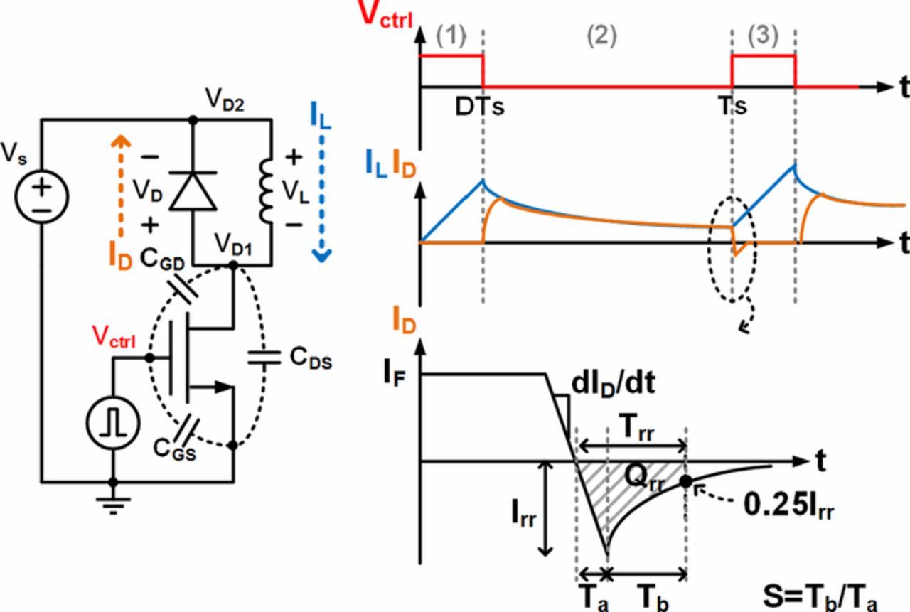
Figure 3. (a) Schematic of switching circuitry (b) voltage and current waveforms of the circuit operations
Moreover, the relationship between the inductor current and the diode current can be expressed as follows:
![Equation ([5])](https://content.cld.iop.org/journals/2162-8777/8/7/Q3229/revision1/d0005.gif)
The decayed current at time Ts determines the diode's forward current (IF). As the power transistor is reactivated (region 3), the Ga2O3 device starts transitioning from the on-state to the off-state. The charges in the diode are removed through a reverse current. After the charge carriers in the diode are removed, the diode is reverse biased to provide a high impedance in the discharge path. Eventually, the current reaches zero. The recovered charge Qrr is proportional to the on-state stored charge, which increases with the forward current ( ) and can be expressed as stated in Refs. 31,32:
![Equation ([6])](https://content.cld.iop.org/journals/2162-8777/8/7/Q3229/revision1/d0006.gif)
where Trr is the reverse recovery time, Irr is the peak reverse recovery current, and S is the snappiness factor (also called softness factor), which is determined by the diode construction and the test circuit environment. According to Equation 6, the Irr and Trr can be derived as follows:
![Equation ([7])](https://content.cld.iop.org/journals/2162-8777/8/7/Q3229/revision1/d0007.gif)
This equation shows how the forward current (IF) and current switching rate (dID/dt) affect the reverse recovery behaviors. The IF and the dID/dt can be controlled with the setup of the test board, such as the pulse voltage, pulse duration, inductor values, and quality factor of the inductor. Trr and Irr are simulated using a circuit simulator with the extracted Ga2O3 Schottky diode model to verify the switching characteristics. Figure 4 is the simulation of these factors on how to influence the diode reverse recovery behaviors. Regarding the simulation setup, the reverse bias voltage is −900 V, the inductance is 15 mH (Q is about 55), and the transistor is driven by a 10V, 2% duration, 50-μs period pulse signal.
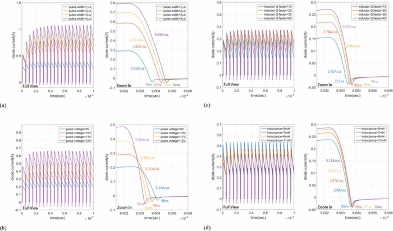
Figure 4. Simulation results of the effects of (a) pulse duration, (b) pulse voltage, (c) Q factor of the inductor, and (d) inductance of the inductor on the Trr.
Figure 4a shows the simulated effects of the duty cycle. The duty cycle is from 2% (1 μs) to 8% (4 μs), and the resulting dID/dt and Trr are from 3.11 A/μs to 4.19 A/μs and from 76 ns to 54 ns, respectively. The duty cycle defines the inductor charging time as it relates to the number of accumulated charges stored in the inductor. The longer the on-time of a pulse, the larger the integral forward current. Figure 4b shows the simulation results of the driven voltage from 9 V to 12 V; the values of the dID/dt and Trr are from 2.14 A/μs to 5.56 A/μs and from 96 ns to 55 ns, respectively. The high drive voltage to the transistor results in low on-resistance and also provides a large forward current at a fixed on-time of the pulse signal. The current switching rate also increases with the duration of the pulse, which can improve the reverse recovery time.
Furthermore, the off-time of the pulse signal dictates the discharging time, and the amount of forward current before the Ga2O3 diode starts switching from the forward state to the reverse-biased state. Thus, the long off-time causes low forward current and current switching rate. In addition to the control signals, the inductor value and quality factor influence the forward current. Figure 4c shows the simulated effects of the inductor Q factor. The Q factor was from 10 to 40, and the resulting dID/dt and Trr were from 2.62 A/μs to 2.97 A/μs and from 115 ns to 78 ns, respectively. Figure 4d shows the simulation results of the inductance from 5 mH to 11 mH, and the values of the dID/dt and Trr were from 2.9 A/μs to 3.13 A/μs and from 85 ns to 76 ns, respectively. The energy stored in the inductor was proportional to the inductance and the quality factor when the charging time was constant. Therefore, increasing the quality factor and inductance helped increase the switching rate. However, the switching rate should be limited to prevent high current flow in a short time. Besides, at the reverse recovery of a diode, the oscillation at the abrupt switching of the transistor comes from the resonator circuit of the stray inductance and capacitance along with the diode. Figure 5 shows the simulation results of the influence of stray inductance and capacitance. The oscillation may deteriorate the recovery time of the diode and damping ripples in the switching circuits. Therefore, stray inductance should be minimized by shortening the wire connections.
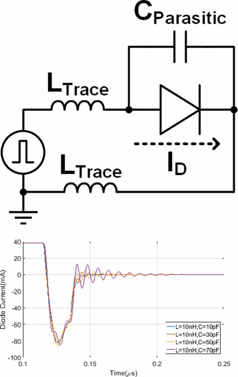
Figure 5. (a) The circuit model of the stray inductance and capacitance from the circuit board and intrinsic diode (b) the simulation results of the damping effects due to the stray parasitics.
In summary, Trr can be reduced by increasing the change rate of the forward current (dID/dt) or decreasing the absolute forward current (IF).31,32 Therefore, increasing the dID/dt helps to reduce the Trr significantly. In contrast, Irr increases with IF and dID/dt. However, increasing the change rate of the forward current would increase the Irr and Vrr, which may destroy the diode and thus limit its recovery speed.
Experimental Results and Discussion
Figure 6 depicts the measurement setup and the circuit board. The fabricated Ga2O3 rectifier was placed on the probe station and wire-connected to the readout PCB for characterization of the reverse recovery dynamics. Figure 7 shows the switching performance of the rectifier. The reverse breakdown voltage of the proposed rectifier was 1711 V. The switching parameters were measured with a forward current of 0.3 A, and the voltage was switched to −900 V. The reverse recovery time was defined as the time required to recover to 25% of the current level of Irr. The fabricated Ga2O3 Schottky diode achieved a reverse recovery time of 81 ns, an Irr of 38 mA, and a dID/dt of 2.5 A/μs. During the switching measurements, the pulse used to drive the Si transistor was operated at a period of 50 μs with a duty cycle of 1 μs. The drive voltage of 10 V was applied to the gate of the transistor while the supply voltage was 900 V. Fig. 7b shows the simulation results, which fits the measurement results by adding the cable and trace parasitics with the diode model in the simulation. The extracted stray inductor is about 800nH and 100nF, including the cable and large trace for accommodating large current flowing to the inductor and diode. The design demonstrated a fast recovery response at a very high voltage for the power-switching Ga2O3 Schottky diode. Table I shows the performance comparison with the state-of-the-art Ga2O3 Schottky diode. The design can achieve a high breakdown voltage and demonstrates a switching voltage up to 900V while Trr. is less than 100ns. The careful design to reduce the parasitics on the PCB and cables are required for optimizing Trr. of the Ga2O3 Schottky diode.
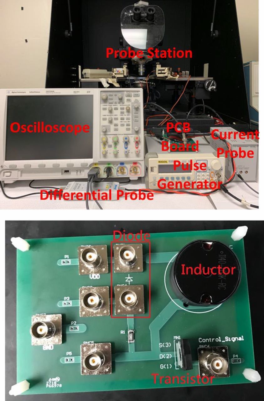
Figure 6. Pictures of the measurement setup and the circuit board.
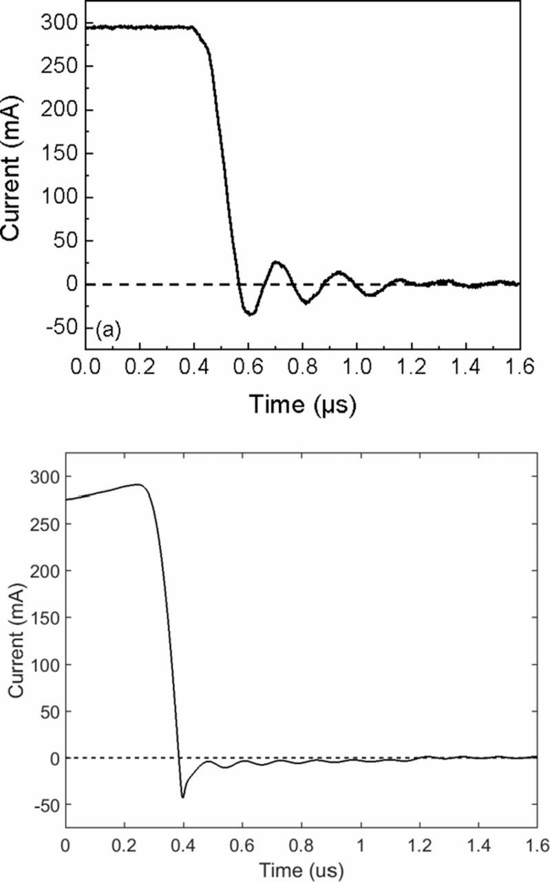
Figure 7. The switching performance of the Ga2O3 Schottky diode using the designed circuit board: (a) measured reverse-recovery time versus (b) simulation results.
Table I. Performance summary and comparison with other Ga2O3 Schottky diode works.
| J. Yang23 | J. Yang25 | A. Takatsuka27 | This work | |
|---|---|---|---|---|
| Material | β-Ga2O3 | β-Ga2O3 | β-Ga2O3 | β-Ga2O3 |
| Breakdown voltage | 2300V | 760V | 300V | 1711V |
| Switching performance | Trr = 22ns@from +2V to −2V | 1 Trr = 11ns @from +10V to −35V 2 Trr = 64ns Irr = 0.82A @IF = 1A, VR = −300V | Trr = 7.6ns Irr = 0.42A@IF = 1A, VR = −100V | Trr = 81ns Irr = 38mA@ IF = 0.3A, VR = −900V |
Conclusions
In this paper, a high breakdown voltage vertical Ga2O3 Schottky diode was fabricated on a 20-μm thick Si-doped n-type Ga2O3 drift layer that demonstrated a 1711 V breakdown voltage and an 81 ns reverse recovery time at a −900 V reverse voltage. A switching circuit using discrete components was implemented in order to achieve a high-voltage switching performance. The design flows, device model and circuit design were analyzed to realize a switching board with the fabricated Ga2O3 Schottky diode. Using this Ga2O3 Schottky diode design that can operate at a high switchable voltage of up to 900 V brings practical power electronics applications a step closer.
Acknowledgments
The authors would like to thank the Ministry of Science and Technology, Taiwan, for their financial support under the grants MOST 107-2918-I-009-010 and 108-2636-E-009-008. The project at the University of Florida was funded by the Department of Defense, Defense Threat Reduction Agency, HDTRA1-17-1-011 monitored by Jacob Calkins and by NSF DMR 1856662 (Tania Paskova). Research at NRL was partially supported by the Office of Naval Research, under contract N0014-15-1-2392. Research at Novel Crystal Technology is partially supported by ONR Global with grant # N62909-16-1-2217.
ORCID
Fan Ren 0000-0001-9234-019X
Jenshan Lin 0000-0002-7439-9259
S. J. Pearton 0000-0001-6498-1256
Marko J. Tadjer 0000-0002-2388-2937
Yu-Te Liao 0000-0002-6868-6729