Abstract
The electroplating of copper by the damascene process is the predominantly used technique for on-chip wiring in the fabrication of ultra-large scale integrated microchips. In this process, void-free superconformal filling of trenches is achieved by multicomponent electrolytes, containing chloride and organic additives in addition to the Cu ions. In this paper we review studies of the atomic-scale Cu interface structure and homoepitaxial Cu electrodeposition behavior in acidic (pH 1–3) Cl-containing electrolyte by in-situ surface X-ray diffraction. This technique provides detailed insight on the 3D atomic arrangement at the electrode surface and fast time-resolved data on the kinetic growth mode. On Cu(111) a complex potential-dependent adlayer structure is found, involving transitions between a chemisorbed oxygen species to a hexagonal close-packed incommensurate chloride adlayer. In contrast, on Cu(001) a simple disorder-order transition to a c(2 × 2) Cl adlayer is found. Parallel to the latter, a crossover from step-flow to layer-by-layer and finally 3D growth occurs during Cu(001) electrodeposition, indicating a decreasing Cu surface mobility toward more positive potentials. The presence of the organic additive polyethylene glycol (PEG) stabilizes the partial c(2 × 2) Cl adlayer on the Cu(001) surface and leads to an inhibition of Cu deposition with a tendency to rougher growth.
Export citation and abstract BibTeX RIS

This is an open access article distributed under the terms of the Creative Commons Attribution 4.0 License (CC BY, http://creativecommons.org/licenses/by/4.0/), which permits unrestricted reuse of the work in any medium, provided the original work is properly cited.
The metallization of microelectronic components by copper damascene plating is arguably the most important electrodeposition process developed in the last decades. Its further development requires better fundamental understanding of the underlying atomic scale mechanisms, which has been a topic of intense research. The central characteristic feature of damascene plating – superconformal filling of nanoscale trenches in the substrate electrode – is achieved by using acidic Cu2+-containing plating baths with several different additives.1–5 In the simplest case, chloride ions in varying concentrations, a polymer that inhibits Cu deposition, most commonly polyethylene glycol (PEG), and an organic catalyst that locally accelerates the deposition in the presence of the inhibitor, such as 3-mercapto-1-propane sulfonic acid (MPSA), are employed. In addition, further organic compounds are often added as levellers and brighteners.
Most studies of damascene plating rely on a combination of electrochemical measurements and ex-situ electron microscopy to determine the evolution of the deposit morphology during growth. These showed phenomenologically the influence of different inhibitor and accelerator species and revealed a strong interdependence of all electrolyte species. In addition, in-situ spectroscopy and ellipsometry were used to study the adsorbate layer on top of the growing Cu deposit, providing a detailed picture of the interplay of halide adsorbates and organic additives.1–3,6 On the basis of these results, thermodynamic data, and numeric simulations, different growth models were suggested.1,2 However, the precise microscopic mechanisms by which the different adsorbates on the Cu surface interact and affect the elementary atomic-scale steps of the growth process could not be assessed by these methods.
A better understanding of these fundamental processes can be obtained by in-situ methods that provide surface structural data on the Cu-electrolyte interface, specifically scanning tunneling microscopy (STM) and surface X-ray diffraction (SXRD). Both techniques have been employed for characterizing the atomic-scale interface structure and electrochemical Cu growth on well-defined single crystal electrodes, each with its distinct advantages and disadvantages. They allow not only investigations of static interfaces, but also under dynamic conditions, which – in the most advanced studies – can approach those in actual plating baths.
Furthermore, the results obtained in such in-situ studies can be directly compared with the vast body of data on Cu surface structure and homoepitaxial deposition under ultra-high vacuum (UHV) conditions. In this environment, Cu growth has been widely studied by STM and scattering techniques. Depending on crystal orientation, deposition rate, and temperature, (i) multi-layer or three dimensional growth, (ii) layer-by-layer growth, and (iii) step-flow growth was found.7,8 These kinetic growth modes and the morphology of the resulting film depends to a large extent on the intra- and interlayer Cu surface diffusion and thus provide insights into the latter.9 However, homoepitaxial growth studies in UHV almost exclusively have addressed growth on clean Cu surfaces. In contrast, Cu electrodeposition is influenced by the presence of adlayers, containing ions and additives from the electrolyte, and by the electrode potential, which can alter the Cu surface transport and the resulting growth behavior in electrochemical environment. Unravelling these effects is a central concern of in-situ studies of electrodeposition processes.
In this review, we focus on the use of SXRD using synchrotron X-ray radiation for static and dynamic studies of the atomic structure of Cu single crystal surfaces and Cu electrodeposition in chloride-containing electrolyte. SXRD is still a more rarely used in-situ method, despite indisputable benefits for such studies. We therefore first briefly introduce into the method and its advantages as compared to competing techniques. Subsequently, we discuss the potential-dependent surface structure of Cu(111) and Cu(001) in chloride-containing acidic electrolyte and, finally, the homoepitaxial electrodeposition on Cu(001) in such electrolyte. In these chapters, we also address the effect of PEG on the interface structure and growth behavior.
Static and Dynamic in-situ Surface X-ray Diffraction Studies
It is beyond the scope of this article to provide a comprehensive description of SXRD and we refer the reader to reviews of the technique.10–14 Briefly, the beam of incident X-rays is scattered at the electrons of the sample and this scattering is measured as a function of the orientation of the sample and the X-ray detector (Figure 1a). Spatial correlations in the sample lead to interference of the individual scattered X-ray waves, resulting in a modulation of the measured intensity distribution (e.g. sharp Bragg peaks in the case of a perfect 3D crystal lattice), which conveniently is described and analyzed in reciprocal space. For scattering at the surface of a crystalline solid, scattered intensity is found along lines which are oriented perpendicular to the surface and arranged in a 2D lattice that reflects the in-plane geometry of the surface (Figures 1b and 1c). For describing these crystal truncation rods (CTRs), typically coordinate systems are chosen where the vector components qx and qy in reciprocal space (denoted by indexes H and K) are in the surface plane and the component qz (denoted by L) is oriented along the surface normal, i.e. along the CTRs. From quantitative measurements of the L-dependent intensity distribution along the CTRs detailed information on the atomic arrangement near the interface can be obtained, including the spacing of the atomic layers, the occupancy of these layers by atoms, the average displacements of the atoms from the equilibrium positions, and the surface roughness. Additional superstructure rods are observed for adlayers with a symmetry different from that of the underlying bulk crystal lattice, allowing to probe the scattering from the adlayer independently from that of the substrate. By combined analysis of several CTRs and superstructure rods the full 3D atomic interface structure can be obtained with up to picometer resolution.10,12,15

Figure 1. (a) Schematic experimental setup of in-situ electrodeposition studies by SXRD, illustrating the diffraction geometry with incoming and diffracted X-ray beam (orange), 1D detector, and the employed electrochemical transmission. Reciprocal space geometry of (b) Cu(001) and (c) Cu(111).
The structural detail of such studies is unsurpassed by other techniques suitable for in-situ studies, but some limitations exist. First, the scattering from light elements is weak, making the localization of species such as oxygen or carbon atoms difficult, in particular in electrochemical environment, where the contrast to the bulk electrolyte is low. However, the adsorption of such species is often accompanied by positional changes of other, more strongly scattering atoms, e.g. those of the substrate, allowing indirect detection. Second, the structure of isolated local defects, e.g. steps or adatoms, is usually not accessible, unless their density is high. Third, a prerequisite for determining the in-plane arrangement of adsorbates is long-range order. However, even for disordered adlayers structural information along the surface normal direction (e.g. average spacings and adlayer densities) can be obtained by measuring the intensity of the reflected X-ray beam (also called specular CTR). Finally, the high X-ray intensity available at modern synchrotron sources may lead to radiochemical changes of the sample and surrounding environment. For this reason, possible effects of the X-ray beam on the interface structure have to be carefully evaluated by control experiments and minimized by suitable adaption of the experimental parameters (e.g. the X-ray flux).
For in-situ studies of electrochemical interfaces the sample has to be mounted inside a suitable electrochemical cell. In the studies reviewed in this paper a cell design using a transmission geometry was employed, where the beam travels through the electrolyte volume of several millimeter thickness (schematically shown in Figure 1a). Compared to more commonly used thin-layer cells,16,17 this geometry provides unrestricted mass transport and a low cell resistance which are vital for high-quality in-situ investigations of electrochemical growth processes under realistic reaction conditions, i.e., at high deposition rates. The cell is formed by two separated compartments and holds a volume of approximately 1 ml electrolyte. The upper compartment contains a Ag/AgCl (3 M KCl) reference electrode which is separated from the bulk electrolyte via a liquid bridge and incorporated into the electrolyte inlet. The lower compartment contains a Pt-sheet as a counter electrode, incorporated into the electrolyte outlet, and a glass capillary. A thin tube, serving as Luggin capillary, is leading from the upper through the lower compartment, stopping about 4 mm above the electrode surface. The X-ray beam passes through an almost cylindrical freestanding meniscus of electrolyte, established between the electrode surface and a glass capillary. In grazing incidence geometry and with a meniscus volume of ∼50 μl, the sample passes through ∼7 mm of electrolyte. For X-ray energies ≥25 keV, this results in less than 25% absorption of the X-ray beam intensity by the liquid. The electrochemical cell is a standard three electrode configuration with a platinum sheet as counter electrode. In addition inner and outer tube also serve as inlet and outlet for the electrolyte, respectively, allowing adjusting the meniscus size and electrolyte exchange during the experiment via a remotely controlled syringe pump system. The successful applicability of this set-up for high quality electrochemical and in-situ SXRD studies was shown with studies of homoepitaxial deposition on gold electrodes.18–20
A key challenge for studies of electrochemical processes, in particular homoepitaxial growth of noble metals, is the high reversibility and fast reaction kinetics. In contrast to growth studies under UHV conditions, where deposition can be quickly terminated by stopping the flux of atoms to the sample, either electrochemical deposition or dissolution occurs, depending on potential. Even at the equilibrium potential both of these processes proceed with high rate, which may lead to rapid structural changes. Conventional SXRD measurements require several minutes for recording a single CTR and 1 to 2 hours for a full CTR set, suitable for detailed structural analysis. While the latter is possible for static interfaces, measured in the double layer range in the absence of electrode reactions, other approaches are required to study the interface during potential changes or under the more dynamic conditions described above. The most simple method for this are potentiodynamic measurements, where the scattered X-ray intensity is measured as a function of time at a specific point in reciprocal space, typically on a CTR far away from the Bragg peaks or at a superstructure rod, while the potential is cycled, scanned or stepped. These can give information on structural changes during adsorption or deposition processes, providing insight into the interface dynamics and intermediate phases at the surface.21,22 For example, the potential dependence of the scattered X-ray intensity from an ordered surface layer with a different symmetry to that of the underlying bulk crystal (e.g. a surface reconstruction or adlayer) directly indicates the potential range of stability of the structure and its potential-dependent coverage. Parallel or subsequently measured cyclic voltammograms (CVs) can be directly correlated with these X-ray data.
More detailed information can be obtained by performing this type of experiment sequentially at different reciprocal space positions and correlating the obtained data. This may even allow reconstructing whole CTRs, providing in-depth structural data with sub-second time resolution.19 Even more significant advancement have recently been made through the availability of fast photon-counting 1D and 2D X-ray detectors. These not only allow following processes at one specific point in reciprocal space but make it possible to record whole diffraction peaks, giving access to peak widths and positions, background signal and, combined with X-rays of very high photon energies, extended areas of the reciprocal space.23–25 In addition, these devices offer faster data sampling with acquisition times of a few milliseconds, which is essential to follow deposition and dissolution rates approaching those employed in technological processes. As the scattered intensities at the surface sensitive positions are low, being able to integrate the scattered, background corrected intensity of the full reflection is of advantage. Such a setup was employed to study the dissolution of Au(001) at rates up to 20 ML/s using a one-dimensional X-ray detector (Dectris Mythen 1K), which allows sampling rates of 600 Hz (compared to ∼10 Hz accessible with NaI point detectors, the standard detector up to ca. 2000).26 The same setup, with the 1D detector oriented in the surface plane (see Figure 1a), was employed in the Cu electrodeposition studies, allowing simultaneous recording of the full diffraction peak cross-section with high data acquisition rate. From the recorded data, transients of the peak intensity, the full width at half maximum (FWHM), and peak position were recorded and information on the lateral surface structure could be obtained, which gave insight into the evolution of strain and domain sizes in addition to the growth behavior.
The high time resolution is a clear advantage of SXRD as compared to electrodeposition studies by other in-situ structure-sensitive methods, in particular scanning probe techniques. Although specific scanning probe setups also can reach data acquisition rates in the millisecond regime27–29 the limited mass transport due to the presence of scanning tip usually obstructs studies under conditions involving high current densities, beyond the double-layer range, and substantial atomic mass transport in the electrolyte.30 High time resolution was also demonstrated in recent in-situ electron microscopy studies of Cu electrodeposition,31 but the influence of the beam on the deposition process is significant in these experiments.
In the following, we describe SXRD results for Cu(001) and Cu(111) in Cl-containing acidic electrolyte. Standard bulk coordinates of the Cu(001) surface will be used. The units for H, K and L are a* = b* = c* = 2π/aNN, where aNN = a0/√2 = 2.56 Å (with a0 the standard cubic lattice constant) is nearest neighbor spacing of the Cu atoms and the index L is along the direction perpendicular to the surface. The close-packed (111) surface has a hexagonal unit cell that is defined such that the surface normal is along the (0, 0, L)hex direction and the (H, 0, 0)hex and (0, K, 0)hex vectors lie in the plane of the surface and subtend 60°. Here, the units for H, K and L are a* = b* = 2π/aNN and c* = 2π/(√6 aNN).
Interface Structure of Cu Electrodes in Chloride-Containing Electrolyte
Chloride is ubiquitous in natural and technological environments and thus its adsorption behavior and adlayer structure on metal electrode surfaces has been studied extensively by a variety of techniques.32 Specifically, chloride is an indispensable component of damascene plating baths. Typical copper electroplating baths used in the damascene process contain chloride ion concentrations between 0.2 and 1.5 mM. In the potential regime which is of relevance for the damascene process, the low index surfaces Cu(001), Cu(110), and Cu(111) exhibit well-defined, densely packed Cl− adlayers. We will present a summary of the current knowledge about chloride on the Cu(001) and Cu(111) surfaces, focussing on the results obtained from SXRD studies.
Cu(111) in Cl-containing solution
Studies of the chloride adlayers on Cu(111) electrodes have been reported using a range of ex-situ and in-situ characterization methods. In UHV, chloride forms a coverage dependent adlayer with a uniaxial compressible structure locking into a (√3 x√3) R30° at a coverage of 1/3 ML (monolayer).33 Stickney and Ehlers were the first to report structural data on the chloride adlayer structure on Cu(111) surfaces by ex-situ low energy electron diffraction (LEED).34 They reported a (12 × 12) superstructure with local (√3 x√3) R30° arrangement and a regular array of domain boundaries. Since then further ex-situ LEED and in-situ STM studies have let to suggestions of a (6√3 × 6√3) R30°,35 a (√3 x√3) R30°,36,37 or a uniaxially compressed chloride adlayer.38
Recent SXRD and electrochemical studies of chloride adlayer formation in acidic electrolyte have found a more complex structural behavior.39 Between potentials of −0.12 and −0.28 VAg/AgCl (at 1 mM Cl− concentration), a hexagonal chloride adlayer was found, which was rotated by about 6° with respect to the high symmetry directions of the underlying Cu(111) surface. The rotation angle and chloride-chloride distance showed a nearly linear dependence on the potential with the highest compression and largest rotation angles at the positive end of the potential range. Rotation angles between 5.3° and 6.3° where observed while the chloride-chloride distance varied from 4.17 to 4.13 Å, which is slightly smaller than the distance expected for the commensurable (√3 x√3) R30° structure (d(√3 x√3) R30° = 4.427 Å). The observed compressibility is much lower than those found for halide adsorption on Ag(111) and Au(111)32,40 and closer to the electrocompressibility found for electrodeposited metal adlayers.41–43
At potentials negative of −0.28 VAg/AgCl, neither this incommensurate adlayer structure nor a (√3 x√3) R30° superstructure or uniaxial-incommensurate structures were observed by SXRD. In contrast, in-situ STM observations reported a (√3 x√3) R30° structure down to potentials of about 200 mV more negative,36,37 which was attributed to an ordered chloride adlayer. Due to the lack of lateral resolution of STM no information could be gained on a possible reordering of the Cu surface.
Additional electrochemical characterization of the Cu(111) surface in electrolyte of different chloride concentrations and different pH-values shed more light on the adsorption behavior for potentials at which no direct superstructure could be observed by in-situ SXRD. Specifically, cyclic voltammetry and chronoamperometry indicated coadsorption of chloride with an oxygenated species.44 Three different peaks were observed in the cyclic voltammetry which could be directly associated with the adsorption/desorption of chloride (peak II/II' in Figure 2b), the ordering of the chloride adlayer (peak III/III' in Figure 2b) and adsorption/desorption of an oxygenated species. The chloride adsorption (II,II') and ordering (III/III') peak showed a clear potential dependence on the chloride concentration of the electrolyte and the adsorption/desorption peak of the oxygenated species (III/III') showed a dependence on the pH of the electrolyte solution. The cyclic voltammogram is fully reversible representing steady-state conditions and does not undergo any alterations with time in oxygen-free electrolyte solution. By measuring current transients and fitting those to a nucleation and growth model, the coverage and time constants for these processes could be deduced. Comparison to the in-plane SXRD data39 and measurements at selected positions along the CTRs44 allowed to gain a full picture of the potential-dependent adlayer composition on the electrode surface (Figure 2a). At the most positive potentials the Cu(111) surface is fully covered by a compressible chloride adlayer. In an intermediate potential region chloride and an oxygenated species are coadsorbed, with the coverage of both species depending on potential. The chloride coverage decreases toward negative potentials, while the coverage of the oxygenated species increases. At potentials near the onset of hydrogen evolution, both of these adsorbates are desorbed from the Cu(111) surface.
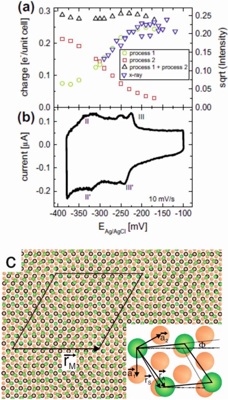
Figure 2. Adlayer phase behavior of Cu(111) in 0.1 NaClO4 + 1 mM HCl. (a) Coverage of chloride (green) and an oxygenated species (red) were deduced from chronoamperometric measurements and compared to the Cl coverage obtained from the intensity of the Cl superstructure peaks (blue). These results show a direct co-adsorption of the two species on Cu(111), which can be linked to features observed in (b) the cyclic voltammogram. (from Ref. 44) (c) Real space structure for the chloride adsorbate (green circles) on the Cu(111) surface (orange circles). The surface unit cells of substrate, (√3 × √3)R30° structure, and the rotated adlayer are shown in the inset. (with permission from Ref. 39).
The process observed in the cyclic voltammogram in chloride containing electrolyte and interpreted in earlier studies as chloride adsorption/desorption45,46 could be identified as the adsorption/desorption of an oxygenated species. Stable adlayers of an adsorbed oxygen species were reported earlier in (chloride free) acidic46,47 and for neutral and alkaline48–50 electrolyte solution. The reversible formation of an underpotentially formed oxide monolayer prior to bulk oxidation was observed. Cu(111) has a binding energy for OH which compared to other transition metals is high and similar to the binding energy for halide ions51,52 which accounts for the possible coadsorption of halides and an oxygenated species. The observed potential dependence indicates that the relative adsorption strength and thus the equilibrium coverage of the two species is potential dependent. Slow adsorption kinetics of the oxygenated species indicate a process involving surface mass transport and a structural rearrangement of the topmost copper layer, though no additional reconstruction peak could be observed by SXRD which could reveal a possible reordering of the Cu surface.
Cu(001) in Cl-containing solution
Most halide adlayers on (001) oriented fcc crystals form commensurate c(2 × 2) adlayer structures, where the adsorbates reside in the energetically preferred fourfold-hollow sites of the metal substrate lattice. For chloride on Cu(001) the c(2 × 2) structure has been reported under UHV conditions53–57 and also found in ex-situ and in-situ studies in Cl-containing electrolyte.58–63 In-situ STM studies could only image the c(2 × 2) adlayer at potentials positive of a critical potential of −0.4 VAg/AgCl for Cl− concentrations of 1 mM. The potential-dependence of the adlayer has been investigated by SXRD for the same chloride concentration. Monitoring the intensity of the superstructure rod at (1 0 0.2) and of the lowest-order CTR at the surface sensitive anti-Bragg position (1 1 0.1) as a function of potential reveals the ordering of the Cl adlayer and the change in Cl coverage, respectively (Figure 3). Three different potential regimes are observed: At potentials positive of E > −0.4 VAg/AgCl up to the potential of copper dissolution, a full c(2 × 2) monolayer with a Cl saturation coverage of θ = 0.5 ML is observed. In an intermediate potential region (−0.4 VAg/AgCl > E > −0.6 VAg/AgCl), the coverage of the chloride adlayer starts to decrease while the c(2 × 2) order in the adlayer still is maintained. At even more negative potentials (E < −0.6 VAg/AgCl), the adlayer is completely disordered, but a significant fraction of the chloride adsorbates remains present on the surface, down to the onset of the hydrogen evolution. The presence of c(2 × 2) order in the SXRD measurements negative of the potential range where the c(2 × 2) structure could be observed by STM is attributed to a high mobility in the adlayer for coverages significantly lower than the saturation value of 0.5 ML. These fluctuations will on the average lead to an equal occupation of the two c(2 × 2) sublattices, leading on the average to a (1 × 1) symmetry within the finite time resolution of STM. Direct support for this could be found in in-situ Video-STM studies, where this was directly observed in the vicinity of highly dynamic c(2 × 2) domain boundaries.64

Figure 3. The potential dependence of the ordered c(2 × 2)-Cl adlayer on Cu(001) can be deduced from the intensity of the Cl superstructure rod at (1, 0, 0.1) (open circles). The Cu CTR at (1, 1, 0.1) (open squares) in addition gives insight into the overall Cl coverage, independent of the ordering. Transitions observed in the potential-dependent X-ray intensity are directly linked to features in the cyclic voltammogram (blue line). The data was obtained in 10 mM HCl as electrolyte solution. (from Ref. 59).
The precise atomic structure of the c(2 × 2) monolayer in the potential regime of saturation coverage was investigated by detailed CTR measurements. This allows the determination of the vertical atomic spacings and thus the bond lengths between the atoms near the electrode surface. A chloride-copper distance of 2.59–2.61 Å was found58,59 suggesting a strong ionic character of the halide-metal bond as this spacing is close to that expected for an in ionic bonding based on the sum of their ionic radii (2.58 Å).65 In contrast, the bond-length deduced from SXRD data of c(2 × 2) chloride adlayers on Cu(001) in UHV53 is closer to that expected for a covalent bonding (2.35 Å). In UHV, also a contribution of the second atomic layer in form of a subsurface buckling has been observed,53 manifesting as an intensity oscillation in the c(2 × 2) superstructure rods (Figure 4a). Here, the second layer Cu atoms below the adsorbed chloride are Δd = 0.012 Å closer to the surface layer than the Cu atoms positioned underneath an unoccupied hollow site.

Figure 4. (a) L-dependence of c(2 × 2) Cl adlayer rod, measured by in-situ SXRD on Cu(001). (from Ref. 82) (b) Top and side view of the c(2 × 2) Cl adlayer structure indicating schematically the subsurface buckling.
Although a similar oscillatory L-dependence of the superstructure rod was observed in electrochemical environment, the exact atomic arrangement at the interface and the contribution of the copper substrate has been controversial. While the very first in-situ SXRD characterization58 did not present any superstructure rods and thus did not allow deduction of the detailed superstructure, later studies found oscillations in the superstructure rod, albeit anti-phase shifted in L as compared to those observed in UHV (Figure 4a). In our own study, we modelled these with a similar oscillation of the subsurface copper atoms, but with an inverted buckling (by Δd = 0.025 Å) where the Cu atoms below the Cl are displaced downward and those below the unoccupied hollow sites upwards (see Figure 4b, bottom).59 The latter was necessary to match the oscillation phase of the L-dependent intensity oscillation. This structure is similar to the one proposed on the basis of in-situ SXRD studies for c(2 × 2) bromide adlayers on Cu(001) electrodes.66 An alternative explanation of the oscillations was suggested by Keller et al., who proposed the presence of laterally ordered layers of water and cations above the layer of adsorbed Cl.60
Further insight into this structure, which may be considered as an exemplary model system for specific-adsorption of anions at electrode surfaces, comes from recent in-situ resonant surface X-ray diffraction studies. In this novel in-situ technique, SXRD measurements are performed at various photon energies near an X-ray absorption edge, which provides local information on the atoms electronic states. The measurements for c(2 × 2) Cl covered Cu(001) showed that the Cu atoms in the second atomic layer have a different electronic structure and thus a remaining charge, depending whether they are located below a halide atom or below a vacant hollow site.67,68 These results support the contribution of the copper substrate to the oscillatory superstructure rod. Furthermore, they specifically allow elucidating the resulting inward pointing dipole moment through the hybridization of the subsurface copper with the halide adsorbate.67
Cu(001) in solution containing Cl and PEG
Surface-enhanced Raman69 and spectroscopic ellipsometry studies70 have shown strong chloride-PEG interaction resulting in the adsorption of a PEG/Cl− layer. Addition of PEG results in a changed cyclic voltammogram with the peak indicating the adsorption/desorption process shifting slightly negative in potential, suggesting that PEG coadsorption induces a slight stabilization of the potential domain in which the Cl adlayer is stable (Figure 5a).71,72 The influence of the organic additive PEG onto the Cl adlayer structure on Cu(001) was investigated by in-situ SXRD, following a modified approach from that described in the section entitled Cu(001) in Cl-containing solution which minimizes the effects of radiolysis.72 This study provided clear evidence of the presence of the ordered c(2 × 2) Cl layer underneath the layer of coadsorbed PEG and of fast, reversible changes of the Cl coverage with potential (Figure 5b). The potential region where the surface was covered by a partial c(2 × 2) adlayer was found to extend to more negative potentials, in accordance with the cyclic voltammetry. In contrast, the fully c(2 × 2) covered surface was reached only at more positive potentials than in PEG-free solution. Thus, the presence of PEG apparently stabilizes an incompletely Cl covered copper surface with local c(2 × 2) ordered chloride adlayer islands. Further structural analysis reveals that the structure of the full c(2 × 2) adlayer is undistinguishable with and without the addition of PEG whereas the partial covered c(2 × 2) layer shows large disorder in the presence of PEG (an increased rms/Debye-Waller Factor). These observations support a microscopic picture where Cl− and PEG coadsorb on the Cu electrode and mutually stabilize each other. They further suggest that this coadsorption may be particularly strong in the (extended) potential range of the partially ordered Cl adlayer, i.e., between −0.6 and −0.3 VAg/AgCl.
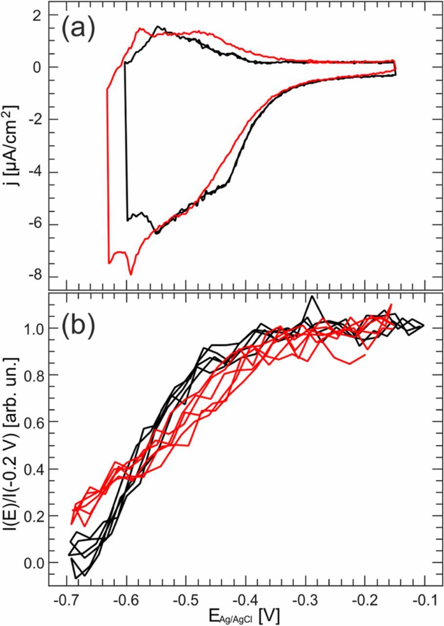
Figure 5. (a) Cyclic voltamogramm and (b) X-ray intensity of the c(2 × 2) superstructure rod at (1,0,0.1) of Cu(001) in PEG-free (black) and 0.1 mM PEG containing (red) 0.1 M HClO4 + 1 mM HCl, recorded at 20 mV/s.(from Ref. 83).
Due to the electron density of PEG and thus the scattering factor being similar, the two cannot be distinguished by SXRD. The stabilization and increased disorder observed in the chloride adlayer hints to a direct interaction of the chloride with the PEG, possibly though a complex formation. The formation of a PEG-Cu-Cl69 or PEG-Cl70 complexes have been suggested earlier by SERS and ellipsometry studies, respectively.
Homoepitaxial Growth on Cu(001)
Growth on Cu(001) in the presence of chloride
In addition to sufficient time resolution, studies during homoepitaxial deposition face another, more general problem, especially if comparison with UHV growth is intended. According to kinetic growth theory, the central parameters that control the resulting morphology in homoepitaxial growth are the flux of adatoms to the growing interface and the rates of surface transport on the growing surface.73 In UHV, both can be easily controlled simultaneously by the evaporation rate of the deposited species and the sample temperature. However, this is different in electrodeposition. Here, the deposition rate decreases at fixed potential until the Nernst diffusion layer has been fully established, which occurs on timescales of about one minute in the transmission SXRD cell used in the experiments. Of course, constant deposition rates can be obtained by galvanostatic deposition, but in this case the potential will change over this time scale. Since the latter strongly affects (i) the composition of the electrochemically adsorbed adlayer, (ii) the rate of surface transport on the electrode surface, and thus (iii) the resulting morphology (see below), controlled studies are not possible this way either. Our solution to this dilemma is to perform the studies under strictly diffusion-controlled conditions, using electrolytes with low metal ion concentrations. In these solutions, we first identify potential regions where the growth occurs via step flow deposition, which maintains and even – after roughening of the surface – allows to reestablish a smooth surface morphology under growth conditions. From this rest potential, steps to other potentials in the diffusion-controlled regime are performed while measuring with time-resolved SXRD the resulting structural changes. This allows growth studies at constant flux of the deposited species, which can be controlled by the ion concentration in the electrolyte, and constant potential. This procedure was developed for studies of Au homoepitaxial electrodeposition18–20,74,75 and used in all studies of Cu growth.
The presence of the halide adlayer on the Cu electrode surface can significantly affect the nanoscale surface morphology and electrochemical deposition behavior. For Cu(001) in Cl-containing electrolyte, already early STM studies revealed a strong influence of the adlayer structure on the orientation of steps on the metal surface. Specifically, a strong faceting of the steps along the [100] and [010] directions was found in the presence of the c(2 × 2) adlayer,62,63,76 which was attributed to an energetic stabilization of those steps by the ordered Cl adlayer. This step faceting is maintained during electrochemical dissolution and deposition at low rates near the equilibrium potential.76,77 The atomic details of the latter processes were revealed by in-situ video STM studies, which directly observed the propagation of kinks along the steps during metal growth and dissolution.28,29 It was shown that kinks of different structure exhibited very different local reaction rates. In particular, the precise arrangement of the halide adlayer at these sites determined the local reactivity.
To determine the influence of the Cl adlayer on Cu electrodeposition at higher growth rates and over a wide potential regime in-situ SXRD growth studies of the type described in the section entitled Static and dynamic in-situ surface x-ray diffraction studies were performed by our group. Here, the homoepitaxial deposition of copper from 0.1 M HClO4 +1 m HCl + x mM Cu(ClO4)2 (for x = 1 and 5) was studied by X-ray transients at the surface sensitive anti-Bragg position (1 1 0.2). Upon stepping the electrochemical potential from −0.6 V, where step flow growth was observed, to more positive potentials, the potential-dependent growth behavior at constant deposition rate could be established.78 These studies revealed transitions between different kinetic growth modes, with a tendency to increasingly rougher growth toward more positive potentials. Specifically, for potential between −0.55 and −0.25 VAg/AgCl oscillations in the intensity at the anti-Bragg position, which are typical for layer-by-layer growth, were observed in 1 mM Cu2+ solution (Figure 6). At the upper end of the potential range, a gradual transition to 3D growth is observed (−0.3 to −0.15 VAg/AgCl), indicated by a reduction in the amplitude of the growth oscillations and a gradual decrease in intensity. From the period of the growth oscillations the deposition rate can be directly determined, yielding 8 ML/min for a Cu2+ concentration of x = 1 mM and 38 ML/min for x = 5 mM. For larger Cu concentrations (x = 20 mM) immediate roughening of the surface by 3D growth was observed even at the most negative potential limit.78

Figure 6. X-ray intensity transients recorded during copper deposition in 0.1 M HClO4 + 1 mM HCl + 1 mM Cu(ClO4)2 electrolyte. The time-dependent intensities at the (1 1 0.1) anti-Bragg position of the Cu CTR (black lines) and the c(2 × 2) superstructure rod at (1,0,0.1) (red lines) were recorded after potential steps from −0.60 VAg/AgCl to the indicated potentials. Oscillations indicate layer-by-layer growth of the Cu surface. (from Ref. 78).
The potential dependent growth behavior can be quantified by comparing the steady state intensity IC at the end of the deposition process to the intensity directly after the potential step IB at the beginning of the deposition process (Figure 7a). The resulting intensity ratio IB/IC (Figure 7b) exhibits a clear change with deposition potential, indicating increasing roughness due to the layer-by-layer to 3D growth transition. This change can be directly related to the chloride adlayer present at the surface. The potential dependent intensity of the superstructure rod at the (1 0 0.1) position in reciprocal space, which is directly related to the coverage of the surface by the c(2 × 2) adlayer, was recorded in copper containing electrolyte and an identical potential dependence of the adlayer as in Cu-free solution could be deduced. At −0.57 VAg/AgCl the order disorder–transition was observed, whereas the saturation coverage into a full c(2 × 2) adlayer is reached at −0.3 VAg/AgCl. The latter correlates with the onset of 3D growth, as can be seen from the decrease in the intensity ratio IB/IC in Figure 7b. In the regime of the fully c(2 × 2) Cl covered surface, the tendency toward 3D growth continuously increases, indicating that the rate of copper interlayer transport gradually decreases toward more positive potentials. This behavior is in contrast to the potential dependence commonly observed for metal self-diffusion, where the mobility usually is higher at more positive potentials. Especially the comparison to the Au(001) electrodeposition in Cl-containing electrolyte show remarkable differences. Here, the in-situ SXRD studies find an opposite potential-dependence of the growth behavior, i.e., a transition from 3D to layer-by-layer and finally step flow growth with increasing potential.75 This is in accordance with STM observations of an increased Au(001) surface mobility toward more positive potentials.79 The anomalous potential dependence of the Cu surface mobility is in good agreement with surface diffusion studies of other adsorbates on the c(2 × 2) Cl covered Cu(001) surface, which also find the mobility decreases with increasing potential, indicating a dominating role of the Cl adlayer. The different behavior in the case of Au(001) may be related to the different nature of the halide adlayers on this electrode surface, which have a quasi-hexagonal in-plane structure32,80 with a more covalent bond and thus a smaller surface dipole moment.68,80

Figure 7. (a) X-ray transient, recorded during a stepwise potential change from −0.5 to −0.6 VAg/AgCl and back in electrolyte of 0.1 M HClO4 + 1 mM HCl + 1 mM Cu(ClO4)2. IB and IC denote the intensity at the start and end of the deposition process, respectively. (b) Intensity ratio IB/IC deduced from transients, recorded for different deposition potentials. A clear decrease in the ratio, indicating development of a rougher surface, can be observed toward more positive potentials. (from Ref. 84).
The interplay between Cl adlayer structure and Cu growth was directly studied by time-resolved studies of the evolution of the c(2 × 2) adlayer during electrodeposition. For this, the intensity of the superstructure rod at (1 0 0.1) was recorded as a function of time in analogous SXRD growth experiments (shown in Figure 6 as red lines). In contrast to Cu-free solution, where the formation of the c(2 × 2) adlayer was observed to be fast (<0.1 s),59 the ordering process is significantly slowed down. Especially in the potential region, where the adlayer eventually reaches the c(2 × 2) saturation coverage (>0.4 VAg/AgCl), the maximal intensity is reached only after ∼20 s. The simultaneously acquired peak width of the superstructure rod decreases parallel to the increase in integrated intensity, showing that the domain size increases together with the overall amount of c(2 × 2) order over this time period.
Similarly, a peak shape analysis of the surface sensitive (1 1 0.1) position of the Cu(001) CTR during the electrodeposition was performed.78 From the in-plane position of this peak the average lateral surface strain at the Cu electrode was deduced. In the potential range of layer-by-layer growth, this strain similar was found to oscillate in phase with the growth oscillations, as also found for homoepitaxial copper deposition in UHV.81 On the basis of a detailed analysis, two contributions to the strain could be identified, which were attributed to strain induced by Cu adatoms and strain at Cu steps. Because the surface densities of both adatoms and steps change during the nucleation and growth of the topmost Cu layer, oscillations are expected for layer-by-layer deposition.
Growth on Cu(001) in the Presence of Chloride and PEG
Similar experiments were carried out to investigate the influence of PEG onto the homoepitaxial copper deposition in 0.1 M HClO4 + 1 mM HCl +1 mM Cu(ClO4)2 + 0.1 mM PEG electrolyte solution under otherwise identical conditions.72 Similar growth oscillations as in PEG-free solution were observed, indicating layer-by-layer growth (Figure 8). However, the oscillation period in the presence of PEG was approximately three times larger as in PEG-free solution, in accordance with the Cu-deposition inhibiting properties of that additive. In the presence of PEG, such growth oscillations are observed between −0.55 and −0.35 VAg/AgCl. Already for potentials larger than −0.4 VAg/AgCl the oscillation become weaker and disappear for potentials positive of −0.35 VAg/AgCl, indicating a transition to 3D growth. This trend is similar to the potential dependent growth behavior observed in PEG-free solution and reflects a reduced Cu adatom mobility toward more positive potentials (see above). However, the presence of PEG shifts the crossover to 3D growth to significantly more negative potentials with the layer-by-layer growth oscillations observed over a wide potential regime, leading to rougher deposits in the potential regime typically employed in damascene plating. This indicates a further reduction of the Cu surface mobility in the presence of PEG, possibly due to formation of surface complexes with coadsorbed Cl/PEG.

Figure 8. Growth oscillations observed at the surface sensitive anti-Bragg position (1,1,0.1) on Cu(001) after potential steps to −0.45 VAg/AgCl in 0.1 M HClO4 + 1 mM HCl + 1 mM Cu(ClO4)2 without (black) and with (red) 0.1 mM PEG. The period of the oscillations caused by layer-by-layer growth significantly increases in the presence of PEG due to inhibition of Cu electrodeposition. (from Ref. 72).
Conclusions
The examples discussed in this review highlight the power of in-situ SXRD methods for the study of electrochemical interface structure and growth processes on the atomic scale. Employing those methods to copper electrodeposition under conditions that are relevant for damascene plating provides in-depth understanding of the interface structure and growth behavior in the electrochemical environment. The obtained data reveal a complex potential-dependent chloride adlayer structure, which pronouncedly varies with the surface orientation. The high structural sensitivity and unsurpassed precision of SXRD allows to detect subtle differences between halide adlayers in UHV and in electrochemical environment, as demonstrated for c(2 × 2) Cl covered Cu(001).
Furthermore, the high brilliance of modern X-ray sources together with progress in X-ray detector technology continuously expand the capabilities of X-ray scattering studies. Specifically, substantial progress in time resolution of the SXRD experiments has been achieved by the implementation of fast one- and two-dimensional X-ray detectors, allowing in-situ SXRD studies of growth and etching processes at the solid-liquid interface at technologically relevant rates. This allows to gain detailed structural information on the interface during growth under realistic reaction conditions, providing fundamental insights into the electrodeposition process. We have illustrated this here by studies of Cu(001) homoepitaxial electrodeposition in Cl-containing electrolyte with and without the organic additive polyethylene glycol (PEG). Operating under diffusion-limited deposition conditions, the influence of electrode potential and deposition rate on the growth behavior could be disentangled. The obtained data show the mutual interdependence of the adlayer structure on the growing surface, the Cu surface transport, and the surface morphology of the resulting deposit. Operando atomic-scale structural studies during electrodeposition with time-resolution in the 100 millisecond range thus contribute to a fundamental mechanistic understanding of the processes occurring during the early stages of growth.
Acknowledgments
The work presented in this paper shows the applicability of SXRD for the study of growth processes for electroplating. An extension of these studies to a much wider range of processes and electrolyte compositions, e.g. including additional additives such as SPS or different plating materials, would be feasible.
ORCID
Y. Gründer 0000-0002-5295-0927