
Abstract
Anodization of TiB2 monolith rather than Ti0 was employed to prepare boron-doped TiO2 photoelectrochemical (PEC) anode and nanocrystals. The anodization behavior of TiB2 was found to be dependent on the orientation of the crystals and F− ions in the electrolyte. TiB2 orientating in [100] direction after anodization in the presence of F− formed a porous TiO2 layer that can be used as a PEC anode, while TiB2 with exposed (001) facets produced a gel containing Ti species in the electrolyte. The PEC anode or nanocrystals from the gel after hydrothermal treatment was boron-doped TiO2 showing superior photocatalytic performance over the counterpart from Ti0 foil for water splitting or Degussa P25 catalyst for dye degradation, respectively. The anodization of conductive ceramic monolith was demonstrated to be a way of preparing doped semiconductors for enhanced photocatalytic performance.
Export citation and abstract BibTeX RIS

This is an open access article distributed under the terms of the Creative Commons Attribution 4.0 License (CC BY, http://creativecommons.org/licenses/by/4.0/), which permits unrestricted reuse of the work in any medium, provided the original work is properly cited.
Photoelectrochemical (PEC) water splitting is a promising approach for the water photoelectrolysis where light is the only energy input for the generation of hydrogen fuel.1,2 Titanium dioxide (TiO2) has also emerged as an excellent material for environmental purification and solar energy harvesting since it was used for water splitting under ultraviolet (UV) light.1,3–5
As the most promising and investigated photocatalyst under UV light, TiO2 with a large bandgap, Eg, of 3.2 eV showed high photocatalytic efficiency.6,7 However, a large portion of the solar energy lies in the visible light, which requires photocatalysts with smaller Eg to increase the efficiency in light photon utilization.8–11 In order to increase the photocatalytic efficiency for visible light, heteroatom doping in TiO2 was performed to increase the light absorption in longer wavelengths than 400 nm.12,13 The C, N or B doping into TiO2 has been achieved to increase the light absorption under visible light and the doping of non-metallic elements was found to generate the occupied density of states (DOS) in the valence band.7,11,14
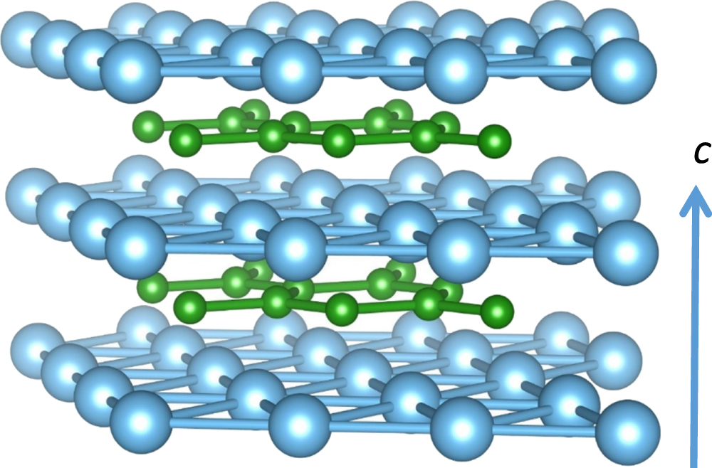
PEC electrode from the anodization of Ti0 foil is a popular method to prepare monocrystalline TiO2.15–18 As an extremely hard material, TiB2 containing metallic bonding showed an electric conductivity of 105 S cm−1.19 TiB2 has the P6/mmm space group hexagonal structure (Fig. 1.) and the Ti-Ti or B-B bonds align in separate planes. The Ti–B ionic bonding is as important as the other bonds in influencing the physical properties of TiB2.20,21 The work function of TiB2 was approximately 4.19 eV, close to Ti metal, 4.33 eV,22,23 but the theoretical calculation predicted that it could vary with crystal planes and terminations.24 Comparing to Ti0, the anodization of TiB2 is much faster in acidic condition and dependent on the dissolved oxygen in the solution.25 However, no attempt has been made on using the highly conductive TiB2 to replace Ti0 to produce a PEC anode through the tunable corrosion behavior of TiB2 under an anodic current that could be interesting to tune the thickness and properties of the TiO2 layer.

Figure 1. Crystal structure of TiB2, where Ti and B atoms are in green and light blue, respectively.
Download figure:
Standard image High-resolution imageIn this study, the anodization of TiB2 was studied to produce a porous TiO2 PEC anode and B doped TiO2 nanocrystals in the meantime without more additional chemicals use. The anodization behavior was found to be dependent on the crystal orientation of the pressed and sintered (PAS) TiB2: a monolith with exposed (100) surface was able to form a TiO2 layer while the one with exposed (001) did not passivate but was able to produce a gel in the solution that, after hydrothermal treatment, is used to produce B-doped nanocrystals. The PEC electrode from TiB2 monolith after anodization showed a photocurrent of 10 times higher than that from Ti0 foil, while the B-doped anatase nanocrystals showed enhanced light absorption than the undoped one. The Rhodamine B (RhB) degradation efficiency from the doped anatase was 4 times higher than the undoped TiO2 under visible light irradiation.
Experimental
A PAS TiB2 monolith (TiB2 > 98.4%, O < 0.8%, C < 0.5% and Fe < 0.1% by weight, Longjitetao New Materials, China) with a 95% density was cut into two orthogonal directions: one was long while the other was normal to the hot press direction, and the two samples were noted as S∥ and S⊥, respectively. The sample is 10 cm × 10 cm × 1 mm in dimensions, giving an active electrode area of 1 cm2. The samples were ground using sandpapers down to 1000 grit, cleaned using deionized water, and dried under flowing air for further use. Silver wires were attached to the back surfaces of TiB2 before they were sealed in epoxy resin for the anodization and electrochemical measurement.
75 ml aqueous solution containing 0.1 M Na2SO4 (99.9%, Keshi, China) and 0.1 M NH4F (99.99%, Macklin, China) or NaF (99.9%, Keshi, China) was used as the electrolyte and a Ti0 foil (99.99%, Goodfellow, UK) as the counter electrode to avoid any contamination from heterogeneous cations. The anodization was performed using a DC power source (M8811, Maynuo power source, China) with a cutting voltage and current of 30 V and 100 mA, respectively. After the anodization, S∥ with a coating on the surface was cleaned using deionized water and annealed at 600 °C for 1 h in the ambient air to increase the crystallinity.26 The thickness of the scale was measured using an ellipsometer (Sopra SE 200 Ellipsometer), while the soluble element after the anodization is measured with an inductively coupled plasma-optical emission spectrometer (ICP-OES, Angilent 5110, USA). The suspension containing the anodic product from S⊥ was transported to a 100 ml PTFE lined autoclave and then treated hydrothermally at 180 °C for 10 h to obtain a precipitated sample that was washed and dried at 80 °C in an oven.
Electrochemistry including cyclic voltammetry (CV) and electrochemical impedance (EIS) was performed on an Admiral Squidstat Plus workstation using a conventional three-electrode system containing an Ag/AgCl reference and Au counter electrode. The scanning rate of CV is 25 mV S−1, and the frequency range of the 10 mV sine wave of the EIS is 1 MHz to 0.1 Hz. A 250 W Xe lamp (HDL-II, Bobei, China, 1 mW cm−2) with a filter to remove the photons under 400 nm and longer than 800 nm was used as the light source for the PEC cell and dye degradation.27 An additional filter was used to remove photons between 400 and 420 nm to evaluate the effect of photon energy on the dye degradation. 100 ml aqueous solution of RhB (10 μM) was mixed with 100 mg powered catalysts from S⊥ via sonication and the mixture was transported to a water-cooling reactor for the illumination. The absorbance at 586 nm was used to determine the concentration of the dye left behind.10
Optical absorption data of PEC electrode and sample powders were collected on a UV–vis spectrophotometer coupled with an integrating sphere (UV-1800, MACY, China). The reference non-absorbing material is BaSO4. Optical microscopy (OM) and scanning electron microscopy (SEM) were performed on an Aosvi metallurgical microscope and a field emission Hitachi S-4800 microscope, respectively. X-ray diffractions (XRDs) of the electrode or powers were measured on a diffractometer (Persee, XD-3, China) with a monochromated Cu Kα target (λ = 1.5406 Å) in a reflective mode. The anisotropy degree (an absolute value)28 and the lotgering orientation factor29 were calculated by XRD analysis to evaluate the crystallographic orientation. X-ray photoelectron spectroscopy (XPS) data were obtained on a ESCALAB 250Xi spectrometer (Thermofischer Scientific, USA) using monochromatic Al Kα X-rays (1486 eV). All binding energies were adjusted according to the energy shift of the adventitious carbon C 1s peak at 284.6 eV.
Results and Discussion
Orientation and morphology
TiB2 contains metal-metal bonding inside the (100) plane and Ti-B covalent bonding along the 〈001〉 direction, and thus the crystal orientation would be important to the physical properties.24,30 The morphology of TiB2 crystals has a significant effect on their physical and chemical properties but is rather difficult to be controlled for specific applications.31 The PAS TiB2 in this study was pressed in two orthogonal directions and the sample cut along the pressing direction, S∥, was found to show extraordinarily high peak intensity of (100) plane from the XRD (Fig. 2). On the other hand, the surface of the sample cut along the free sintering direction, S⊥, was dominated by (001) facet. The orientation of the TiB2 can be validated by the OM images, where darker areas were found in the S⊥ because the ionic bonding in (001) direction would cause the brittleness32 and enhance the roughness of the surface for the dark area, the crystallographic orientation degree along [001] direction (A[001]) was calculated for the S⊥ and S∥ as an absolute value to be 10.13 and 0.84, respectively, and the lotgering orientation factor along [001] direction (f[001]) was 0.697 and 0.072 for the S⊥ and S∥,respectively, which evidence more grains orientation forms for S⊥ in [001] direction.
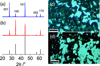
Figure 2. XRDs and the corresponding OM images of S⊥ (a), (c) and S∥ (b), (d). The powder diffraction profile (PDF) of a polycrystalline TiB2 was shown in vertical lines for reference. The bright phase could be the exposed (100) crystal plane. The scale bar is 100 μm.
Download figure:
Standard image High-resolution imageCorrosion electrochemistry
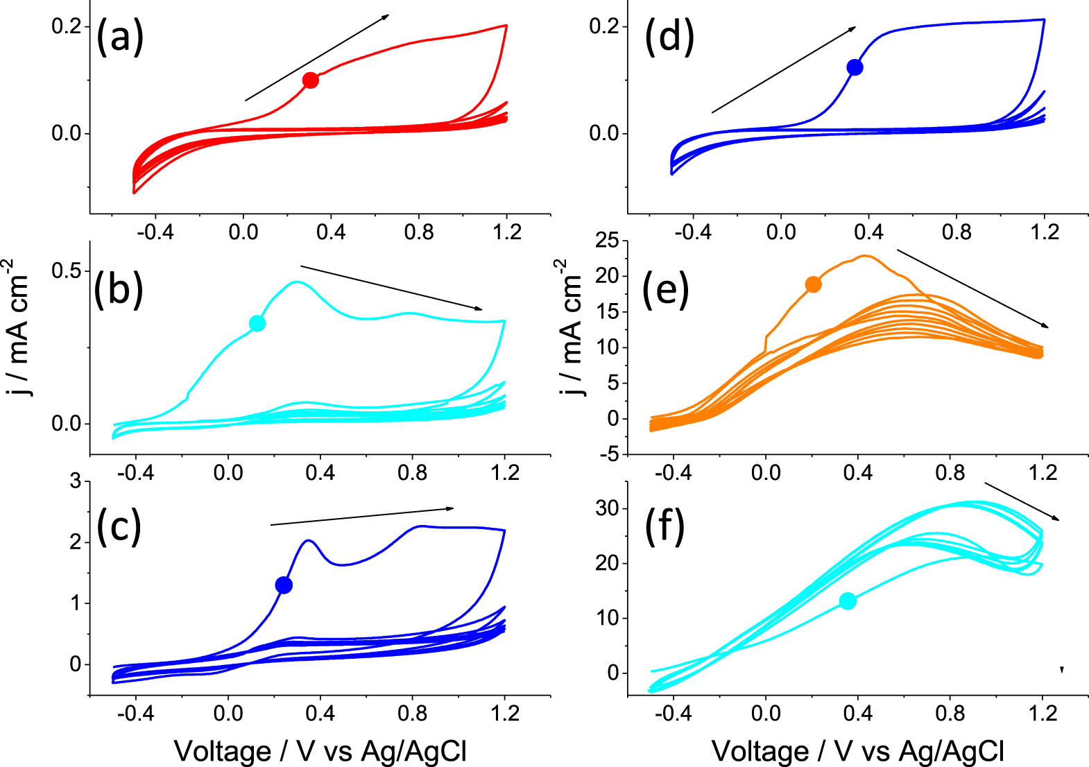
As a PEC anode, the corrosion resistance under working conditions is important for durability. For the Ti (Fig. 3), S∥ and S⊥ showed relatively high current densities in the scan from −0.5 to 1.2 V in the first cycle as a result of the oxidation on the surface. From the second cycle to the fifth cycle, the current densities, j, are much lower than the first cycle indicating a passivation region between 0.2–0.8 V vs Ag/AgCl. The addition of NH4F dramatically changes the corrosion behavior of S∥ and S⊥ but has little influence on that of Ti. Specifically, the S⊥ showed an increased current density in the 2nd ∼ 5th cycles than the first one as a result of the active corrosion. Although S∥ showed a smaller peak current density than S⊥, it did not change the corrosion behavior in F− containing solution, which is in accord that both samples can produce a soluble gel after prolonged corrosion times under anodic current. Nonetheless, the rough surface of S⊥ does not allow the formation of a TiO2 layer for the preparation of the PEC electrode. TiB2 was subjected to localized corrosion on the grain boundary in NaCl solution33 and the fast corrosion of S⊥ was reasonable in our case as it showed finer crystallite due to the brittles of B–Ti bonds and finer grains.

Figure 3. CV of Ti (a), (d), S∥ (b), (e) and S⊥ (c), (f) under 0.1 M Na2SO4 (a)–(c) and 0.1 M Na2SO4 + 0.1 M NH4F (d)–(f). The dots in each plot was used to indicate first cycle.
Download figure:
Standard image High-resolution imageAfter the CV, EIS (Fig. 4) was used to study the surface property and corrosion behavior of the electrode. The EIS of the S∥, S⊥, and Ti showed only one arc in Na2SO4 electrolyte. The EIS of S⊥ was much smaller than those of Ti or S∥ in a neutral Na2SO4 solution. When F− was added to the electrolyte, Ti electrode showed insignificant variation, but the impedance values of S∥ and S⊥ were much smaller than those without F−, indicating an accelerated corrosion rate induced by the F−.34,35 The EIS of S∥ with (001) surface showing two semi-arcs could be related to the formation of a porous film on the surface, while S∥, whose EIS showed only one semi-arc, experienced active corrosion. Therefore, the EIS for samples in electrolyte without and with NH4F can be fitted with an equivalent circuit graphically represented in Fig. 4, and the fitting parameters are listed in Table I.
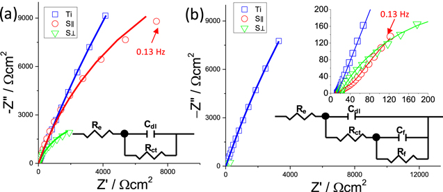
Figure 4. EIS of Ti, S⊥ and S∥ in Na2SO4 electrolyte without (a) and with (b) NH4F at open circuit potential after the cyclic voltammetry. EIS of S⊥ and S∥ in (b) was magnified as inset. The equivalent model circuits for samples with and without NH4F are shown as insets. The simulated data were plotted in lines.
Download figure:
Standard image High-resolution imageTable I. Parameters of the simulated data.
| 0.1 M Na2SO4 | 0.1 M Na2SO4 + NH4F | ||||||||||
|---|---|---|---|---|---|---|---|---|---|---|---|
| Re | Ydl | ndl | Rct | Re | Ydl | ndl | Rct | Yf | nf | Rf | |
| Ω cm2 | Ω−1 Sn cm2 | Ω cm2 | Ω cm2 | Ω−1 Sn cm2 | Ω cm2 | Ω−1 Sn cm2 | Ω cm2 | ||||
| Ti | 13.9 | 1.1 × 10⁻⁴ | 0.77 | 1.4 × 10⁵ | 14.0 | 1.3 × 10⁻⁴ | 0.79 | 1.0 × 10⁵ | — | — | — |
| S⊥ | 20.9 | 3.3 × 10⁻⁴ | 0.76 | 7.2 × 10³ | 19.5 | 3.0 × 10⁻³ | 0.73 | 603.0 | — | — | — |
| S∥ | 12.2 | 8.4 × 10⁻⁵ | 0.80 | 3.5 × 10⁴ | 15.7 | 4.5 × 10⁻³ | 0.72 | 1.3 × 10³ | 2.2 × 10⁻³ | 0.67 | 50.1 |
In the model circuit, Re represents the electrolyte resistance, Cdl the double-layer capacitance, Rct the charge-transfer resistance, Cf the oxide capacitance, and Rf the oxide resistance. Taking into account the dispersion effect, a constant phase angle element (CPE) Q is used to describe the element Cdl and Cf in the fitting procedure. The Ydl and ndl, and Yf and nf are the constants representing the element Qdl and Qf.34,35 As the corrosion rate is proportional inversely to Rct, the comparison of Rct indicates that the corrosion behavior of Ti0 varied little with the addition of F− while the S⊥ corrodes 10 times faster in F− containing electrolyte than the one without. S∥ was the only sample that showed an impedance response from the porous oxide film.
PEC electrode from S∥
TiB2 is very resistant to high-temperature oxidation in air. The oxidation of TiB2 at temperatures below 1000 °C will produce a thin layer of TiO2 covered by B2O3,36 but the direct oxidation at 600 °C for 1 h would be insufficient to grow a film for the photocatalysis.21,36 In our study, XRD (Fig. 5a) of the anodized S∥ sample after annealing at 600 °C for 1 h showed very distinct peaks of rutile- and anatase-type TiO2 without B2O3, indicating that the oxides are produced during the anodization process. According to the ellipsometry, the thickness of the TiO2 on S∥ layer is around 5 μm, which is around 10 times thicker than that on Ti0. Thicker TiO2 (<6 μm) can be produced in ethylene glycol electrolyte with 2 vol% water and NH4F,37 but the thickness of the TiO2 layer is subjected to the operation condition of anodization voltage and its sweeping rate, and F− concentration.15 The retained TiO2 layer during anodization is dependent on the oxidation rate of the substrate and the dissolution process. Generally, the dissolution rate of the produced TiO2 decreases with pH near the substrate/TiO2 interface. The thicker TiO2 layer on TiB2 could be attributed to (1) TiB2 in our case showed much higher anodization rate than Ti0 as indicated in the electrochemical investigation and (2) the concentration of NH4F is 0.1 M, the rate of TiO2 dissolution on Ti0 could be higher than that on TiB2 as the formation of B2O3 in latter could be able to scavenger the H+ near the TiB2/TiO2 interface.

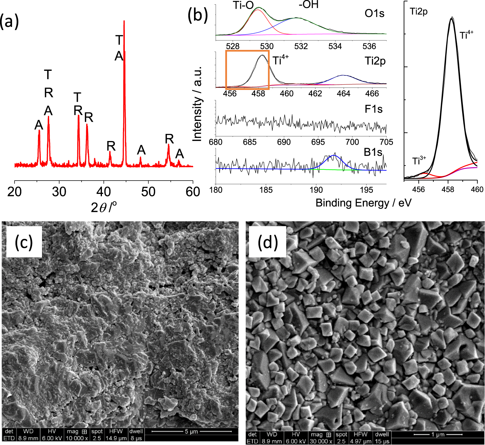
Figure 5. XRD (a), XPS(b) and SEM (c), (d) of the PEC anode from the anodized of S∥ with exposed (100) surface. The core-level scan of Ti2p in rectangle was enlarged in the right side of (b) to show the presence of Ti3+. "T", "A" and "R" in (a) indicates TiB2, anatase and rutile, respectively.
Download figure:
Standard image High-resolution imageThe XPS spectra (Fig. 5b) of the outgrown oxides show an insignificant peak of F1s, but the B1s peak at 191.8 eV clearly indicates the presence of minor interstitial B forming [BO4] units in TiO2.7 The detailed analysis of Ti2p indicates that a small fraction (3.0%) of Ti3+ is produced on the anodic coating on S∥ after the calcination. The O1s peak at the binding energy of 529.5 eV is unequivocally attributed to the O2− in Ti–O bonds while the one at 531 eV is possible resultant from the weakly adsorbed hydroxyl group in Ti–OH.38–40 The oxide layer on S∥ is very rough and porous (Fig. 5c), but the produced TiO2 crystals in the magnified image are in the size of 100–300 nm and show sharp edges (Fig. 5d). The anodic coating on TiB2 did not consist of nanotubes, but Zhen et al.41 prepared orientated TiO2 pillars on Ti0 foil and found that the exposed high-energy reactive facets in rutile boosted the water oxidation reaction by a factor of 2.5.
The TiO2 layer on TiB2 showed a light absorbance edge at 408 nm (Fig. 6a) and the broad arc in the wavelength from 400 nm to 1100 nm could be related to the absorption induced by Ti3+ and defects as shown in the XPS results.16,42–44 The light absorbance edge is 26 nm red-shifted comparing with the TiO2 from Ti0 foil [e.g. 382 nm as reported by Chen et al.45], which could be related to the B doping. The space charge capacitance, Csc, of the TiO2 layer under bias was measured using EIS, and the Mott-Schottky plot (Csc−2 vs bias, Fig. 6b) showed a positive slope and an intersection of −0.57 V vs Ag/AgCl with −0.37 V vs SHE, indicating the TiO2 layer is an n-type semiconductor with a flat band energy, Efb, of −0.37 V vs SHE.46–48 The Efb of the TiO2 on TiB2 is close to with the values of TiO2 nanotubes (−0.23 V vs SHE) from the anodization of Ti.49,50
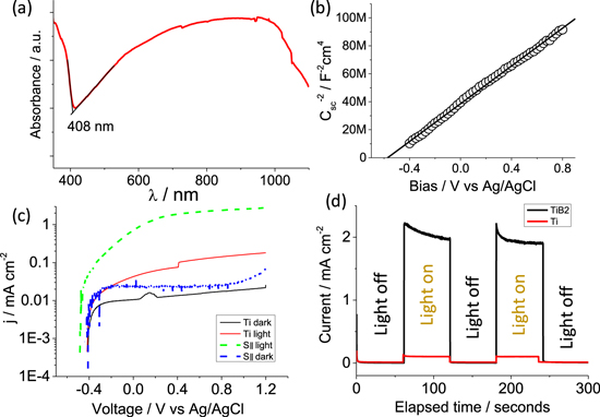
Figure 6. (a) UV–vis spectrum and (b) Mott-Schottky plot of the TiO2 on S∥. (c), (d) the current density variation of anatase TiO2 on S∥ or Ti0 foil under dark or light condition. The bias for the photocurrent in (d) is 0.5 V vs Ag/AgCl.
Download figure:
Standard image High-resolution imageIn accordance with the previous study, Ti0 is more corrosion-resistant under an anodic bias than S∥ in neutral Na2SO4 electrolyte, so S∥ showed a slightly higher current density under dark condition (Fig. 6c). However, the PEC anode from S∥ showed a much higher current density than the counterpart on Ti0 foil if they were illuminated under a 250 W Xe lamp with >400 nm photons. Specifically, PEC anode on S∥ under a bias of 0.5 V showed a photocurrent of 1.96 mA cm−2 (Figs. 6c and 6d), while the one on Ti showed only a photocurrent density of 0.10 mA cm−2. The photocurrent generation with the PEC on S∥ is stable for at least two dark-light cycles. The high photocurrent from PEC on S∥ sample could be related to the thick TiO2 film and B doping to enhance the light absorption or the presence of Ti3+ to ease the charge transfer resistance.51
Nanocrystals From Anodization of S⊥
Anodization of metals has been used for the production of monocrystalline oxides under the ambient condition52,53 and the dissolution of the metal and precipitation of the ionic species in the electrolyte are generally involved for the growth of oxides.54 Under the anodic condition, S⊥ suffers from active corrosion in F-containing electrolytes without any oxide deposition on the surface. A gel in the electrolyte instead as a result of the dissolution and precipitation of Ti and B species was produced in the electrolyte. The concentrations of soluble B and Ti in the electrolyte are measured to be 13.5 mM l−1 and 1.98 mM l−1, respectively, if the solid content of the gel is filtered out.
In order to study the reaction mechanism, XPS of the sample from the drying and washing of the gel, along with those of Degussa P25, hydrothermally-treated solids from electrolytes containing NaF (T-NaF) and NH4F (T-NH4F) (Fig. 7). The solid from the gel after mild drying at 60 °C showed the obvious peak of Ti3+ and this could be related to the oxidation of TiB2 under anodic according to the following reaction:55

Where nine electrons are involved in the reaction. This reaction is in contrast with the ten-electron reaction for the production of soluble Ti4+-containing species:

The presence amount of Ti3+ is conditional and can reach 40% of the anodic reaction in deaerated conditions.25 However, the Ti3+ in the solid gel is estimated to be 4.0% of (Ti3+ + Ti4+) though the fitting of Ti2p in XPS. The low Ti3+ on the surface of gel could be related to the hydrolysis and oxidation in ambient air:

While NH4F was used in the hydrothermally prepared TiO2 with F-doped TiO2,56 Sun et al.57 used boric acid (H3BO3), tetrabutyl titanate and ammonium fluoride (NH4F) as the precursor for the synthesis of B/N co-doped TiO2. As the electrolyte contains F− and ammonia, the possible F- and N-doping in T-NH4F was also studied through XPS (Fig. 7). Because the binding energy of F1s of T-NaF and T-NH4F peaked at 684.0 eV was much lower than that of TiOF2 (685.3–685.5 eV)58 or TiO2−xFx (689.0 eV),42 therefore the F− could be only assigned to the absorbed F− replacing the –OH groups on the surface. The O1s peak for T-NaF and T-NH4F was identical to that of Degussa P25 and the formation of oxide-ion vacancies is minor. N1s peaks at 399.7 eV were found on the XPS spectra for the Degussa P25 and T-NaF, and thus they could be related to the adsorbed N species.59 Nonetheless, we cannot rule out the trace N doping in T-NH4F since the core-level XPS of N is affected by the absorbed species. T-NH4F was the only sample showing a significant peak of B1s at 191.9 eV, corresponding to interstitial B in the tetragonal unit [BO4].7,60 The [B]/([B]+[Ti]) on the surface of T-NH4F was calculated to be 0.5 at% from XPS. The interstitial B doping in the TiO2 crystal will induce the formation of Ti3+ in the oxide lattice:

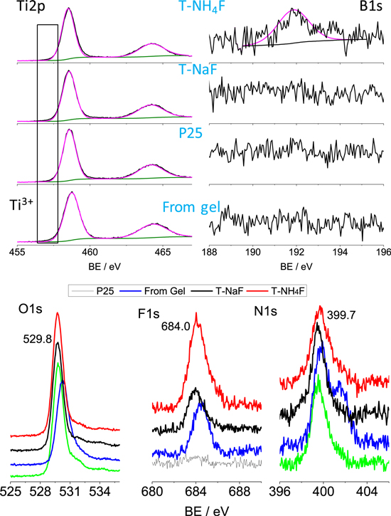
Figure 7. XPS core-level scans (Ti2p, B1s, O1s, F1s, and N1s) of T-NaF and T-NH4F comparing with the product from the dried gel and Degussa P25.
Download figure:
Standard image High-resolution imageThe anodic product of TiB2 was able to produce Ti3+, while the B was oxidized to be BIIIO33− in the electrolyte. During the hydrothermal treatment, B needs to be reduced slightly if the charge of B is smaller than 3. In preparing the B doped TiO2, Lambert et al.61 used TiCl4 under a dry, O2-free nitrogen atmosphere and BH3 in tetrahydrofuran as the reactant to reduce the oxidation of B species or the generated Ti3+ species. The reducing agent for B3+ in the aqueous phase could be Ti3+ and the replacing of NaF with NH4F would assist the reduction process as the latter can scavenge the residual oxygen in the autoclave and reduce the oxidation of Ti3+. The preservation of Ti3+ in the autoclave could in the end increase the B incorporation in titania lattice. The B doping in T-NaF was too low to be detected in XPS.
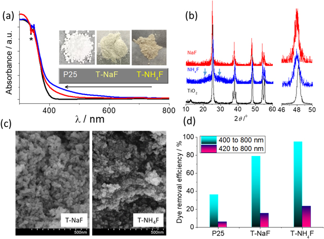
Comparing to the white Degussa P25 whose UV–vis spectra, T-NaF and T-NH4F showed a light absorption tail stretching to 500 and 600 nm (Fig. 8a), respectively. T-NH4F showed deeper color and stronger light absorption in the visible light region than T-NaF as a result of higher B doping in the former. According to the XRD, the crystal structure of both samples was found to be anatase-type TiO2 with a clear decrease in peaks intensity and slight shifting to lower angle suggesting the incorporating of B (Fig. 8b). Anatase is the low-temperature polymorph of TiO2 in contrast with the mixed rutile and anatase in the PEC anode calcined at 600 °C. Uniform particles within the scale of 20–30 nm were found in T-NaF according to the SEM images (Fig. 8c), but the T-NH4F sample showed aggregate of finer crystals (10–20 nm in diameter). The B doping in TiO2 was found to inhibit the crystallinity of TiO262 and this can be also implied from the wide shoulder peak in the XRD of T-NH4F. The RhB removal efficiency from T-NH4F was the highest among the three photocatalysts (Fig. 8d): the removal efficiency of T-NH4F is 2.64 and 4.0 times higher than that of Degussa P25 under 400–800 nm and 420–800 nm irradiation, respectively.
Figure 8. (a) UV–vis spectra, (b) XRD, (c) morphologies, and (d) 1-hour RhB degradation efficiency of TiO2 nanocrystals prepared from the hydrothermal treatment of the suspension from NaF (T-NaF) and NH4F (T-NH4F) electrolyte. The UV–vis spectra in (a) and RhB degradation efficiency (d) of Degussa P25 was provided for comparison. The arrows in (b) indicate the position of a shoulder peak and the peak at a 2θ of 48o 22' was enlarged to highlight the shift of peaks.
Download figure:
Standard image High-resolution image
Conclusions
TiB2 as the most common 2-dimensional transition metal boride was found to be able to produce B-doped TiO2 coating or nanocrystals for efficient photocatalysis. The use of TiB2 instead of Ti0 was able to vary the anodization kinetics under F-containing electrolyte and a porous film of 5 μm in thickness can be obtained in 2-hour anodization. The TiO2 PEC on TiB2 achieved a high photo-current of 1.96 mA cm−2 under irradiation in between 400 to 800 nm. The fast dissolution of TiB2 with exposed (001) facet during the anodization process was able to produce a gel containing Ti3+, which is a metastable state for the synthesis of oxygen-deficient TiO2−x.63 Boron-doped TiO2 after hydrothermal treatment boasted interstitial B that increased the light absorption in the visible light region for efficient RhB degradation. As MBene and Maxene64,65 comprise a large family of electric conductive ceramics, their anodization would be of great importance to the synthesize of cation/anion doped semiconducting oxides for efficient photocatalysis.
Acknowledgments
We would like to acknowledge the support from Natural Science Foundation of China (NSFC, 51702264, 41371275), the Fundamental Research Funds for the central universities (XDJK2020B066). Y.T. thanks to the undergraduate innovation project from Chongqing (S20201063517). C.N. also thanks to the support of Bayu Young Scholar from Chongqing.