
Abstract
In this study, the monodisperse abrasive deposition (MDAD) system was developed to investigate the polishing mechanism of ceria abrasives for the chemical mechanical planarization of a wafer. Using the MDAD system, groups of ceria particles with a specific size were collected from slurry with various particle size distributions, and each group was deposited on a blanket silicon wafer to study the size effect of the ceria particle on polishing results. The effects of the ceria particle size on surface roughness, contact area ratio, and subsurface damages on the surface and subsurface crystallographic structure were investigated using atomic force microscopy, transmission electron microscopy, and a surface inspection system. A similar set of experiments was performed with types of ceria abrasive particles with the same diameter but different morphologies to investigate the effect of the ceria abrasive geometry on polishing results. In addition, the effect of the ceria particle size on the pattern loading was investigated by polishing the shallow trench isolation and high aspect ratio patterned wafers.
Export citation and abstract BibTeX RIS
A chemical mechanical planarization (CMP) process is widely used for planarization and node separation of metal and dielectric films to realize a multilevel layer.1, 2 During the CMP process, a rotating wafer is pressed face down onto a rotating resilient polishing pad, where the polishing slurry containing abrasive particles and chemical reagents carries out the material removal and polishing of the wafer surface.3 Recently, the semiconductor industry has tried to change the polishing medium from the conventional silica-based slurry to the ceria  -based slurry. The ceria abrasives offer merits such as high removal rate and high selectivity with polymer additives and exhibit no slurry agglomeration with pad lifetime.4, 5 However, the high scratch level and pattern loading effect of ceria abrasives at the initial stage of CMP in device patterning have limited their use.6 There is insufficient knowledge of the nature of the contact phenomena between the ceria abrasive and the polishing layer. Therefore, the nature of the polishing characteristics of the ceria abrasive with large particle size distributions needs to be understood in detail.7
Many researchers have taken different approaches to understand the relationship between the CMP process performance and the size of silica  particles utilizing the concept of a two-body wear mechanism between the slurry abrasives and the wafer. Also, researchers showed that the material removal rate depends on the mean size of active silica abrasives, of which the larger abrasives yield a higher removal rate by a deeper indentation.8–13 Some results also showed that the oversize particles of the silica abrasive were the source of microscratches.14, 15 To quantify the effect of the abrasive size, colloidal silica
  of a uniform particle size distribution is typically used.16 But there is only a limited amount of research related to the relationship between the polishing mechanism of the ceria abrasive and abrasive size, which did not consider the quantitative and fundamental characteristics of the ceria abrasive.17
In this work, the polishing characteristics of the ceria abrasive are investigated according to particle size. To examine the polishing mechanism of the CMP as a function of the ceria abrasive size, monosize ceria abrasives were used. The monodisperse abrasive deposition (MDAD) system with scanning mobility particle spectroscopy (SMPS) was developed to use the monosize ceria abrasive in the polishing process. Furthermore, the effect of the ceria abrasive on the pattern loading was examined. Based on our results, guidelines for achieving the required high performance of the semiconductor CMP process using the ceria slurry are provided.
Experimental
The MDAD system was developed to quantify the polishing characteristics of the ceria abrasive. Monosize particles can be deposited on a substrate using the MDAD system. Figure 1 shows the schematics of the MDAD system. It mainly consists of three components: the atomizer, the differential mobility analyzer (DMA), and the deposition chamber. When the CMP slurry was diluted with deionized (DI) water in the atomizer, the slurry transformed from colloidal to aerosol. The aerosol-type slurry flowed into the DMA. In DMA, the specific sizes of the abrasives can be sorted using the electrical mobility corresponding to each abrasive size. The electrical mobility corresponding to an abrasive size can be defined by the relation between the electrostatic force and the drag force of the abrasive.18 Figure 2 shows the calibration result of the sizes of the collected ceria abrasive as a function of DMA voltages. With the MDAD system, four different sizes of the ceria abrasive ranging from 30 to 400 nm were sorted, and each group was deposited on a conventional 8 in. wafer. A condensation particle counter (CPC) was used to measure the number of deposited particles. The wafers were polished with a polishing system (Applied Material MIRRA) using an IC1010 pad (Dow Chemical). During the polishing, only the DI water flowed onto the pad surface, and the table and head rotation speeds were at 10 and 100 rpm, respectively. Polishing was performed for 30 s. The head pressure was set at 3 psi. The structural damage and surface roughness of an 8 in. silicon bare wafer were examined according to various abrasive sizes. A similar set of experiments was performed with three ceria abrasive particles, which had the same diameter of 200 nm but with different morphologies to investigate the effect of the ceria abrasive geometry on polishing results. The removal performance of the ceria abrasive was investigated with varying abrasive sizes for two shallow trench isolation (STI) patterns and the dynamic random access memory (DRAM) device with a high aspect ratio. The active pitch of the STI patterns was 500 nm, and the trench depth was 300 nm. The step height in the high aspect ratio pattern was  , and the length of the top area was 100 nm. After polishing the wafer with abrasives of different sizes, the wafer surface integrity was measured using atomic force microscopy (AFM, SPA400, Seiko Instrument, Japan). The surface roughness was measured at 10 sites of
  . The values reported in this study were the average of the root-mean-square surface roughness calculated at these 10 sites. Subsurface structures of the polished specimens were studied in transmission electron microscopy (TEM, JEOL 2010, Japan) modes to directly observe the transition of silicon from its initial crystalline structure to an amorphous state. Also, the surface topography of the polished specimen was checked by the wafer surface inspection system LS6800 (Hitachi Co., Japan).
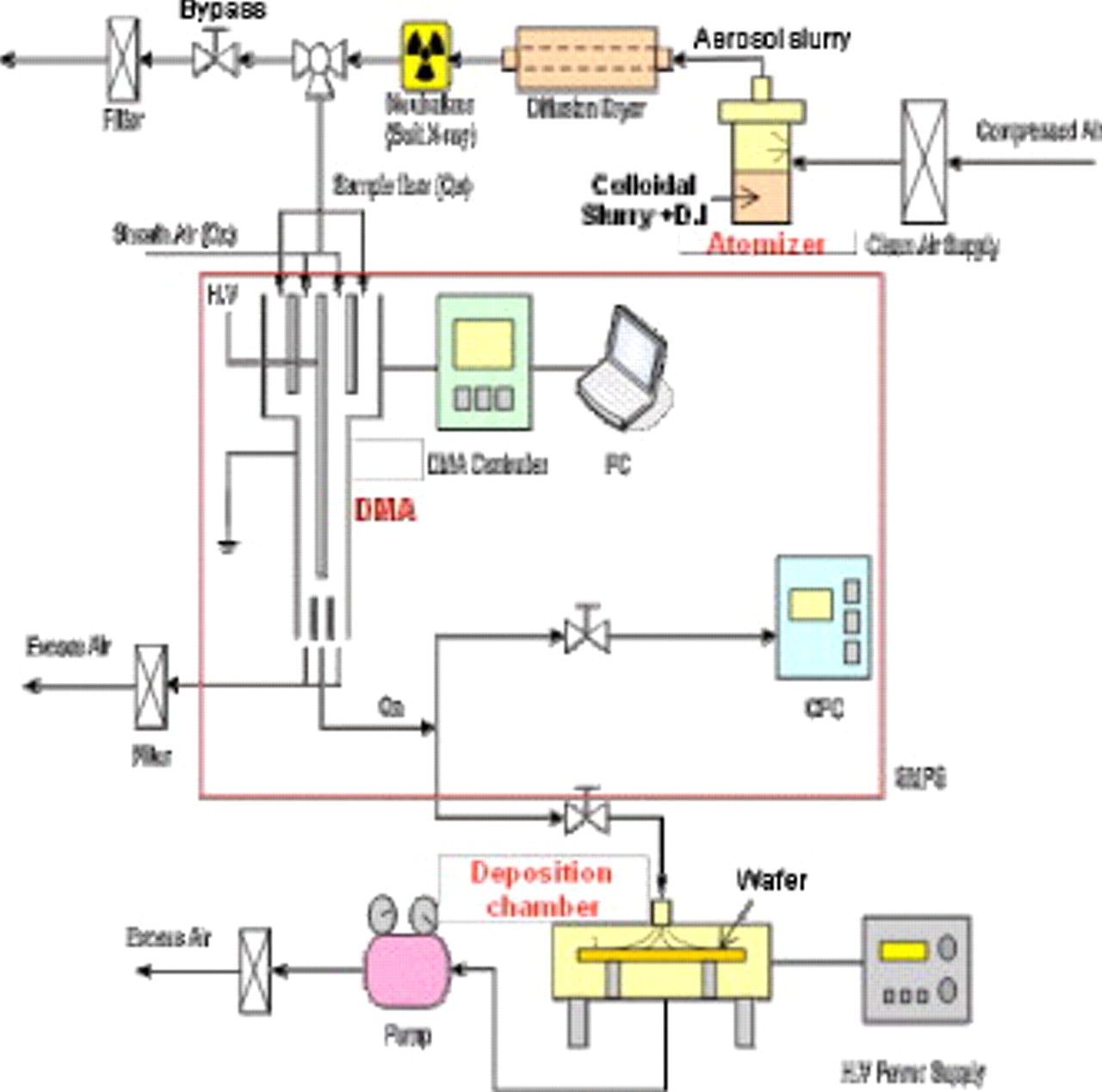
Figure 1. Schematics of MDAD system mainly consisting of atomizer, DMA, CPC, and deposition chamber.
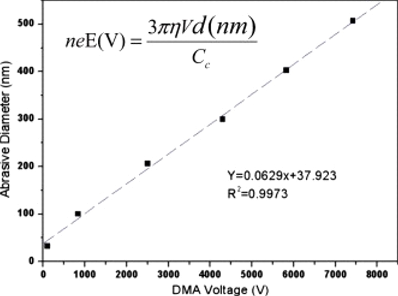
Figure 2. Calibration result of DMA voltages and collected ceria abrasive size.
Results and Discussion
Ceria abrasives of a designated size were deposited on the wafer using the developed MDAD system. Figure 3 shows the results of the abrasive size distribution obtained by SMPS 19 and the abrasive shape corresponding to each size obtained by scanning electron microscopy (SEM) measurements. We obtained specific abrasives (30, 100, 200, 300, 400, and 500 nm) in various size distributions of the ceria abrasive. The MDAD system can be used not only to obtain the specific abrasive size but also to examine the surface morphology of a single abrasive. The large-sized abrasive, known as the secondary particle, was composed of agglomerated primary crystalline of ceria. According to the SEM image of the abrasive of each size, it can be speculated that the agglomerated form of the ceria abrasive is not a physically agglomerated form but a chemically agglomerated form. So, each particle of the ceria abrasive as a spherical was assumed as a spherical object in the contact model. The elements of deposited particles were also confirmed by SEM/energy-dispersive X-ray (EDX) analysis. As shown in Fig. 4, the spectrum of EDX in the abrasive shows only cerium and oxygen.
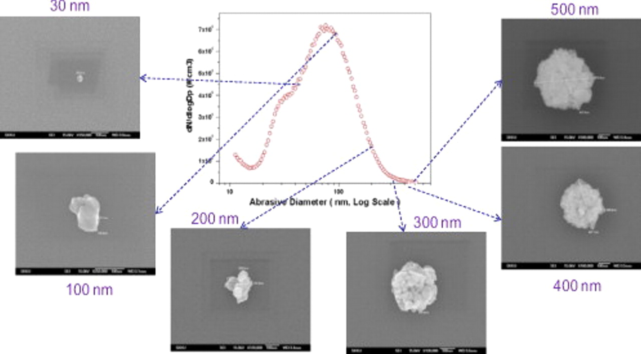
Figure 3. Abrasive size distribution and shape of each size of ceria abrasive.
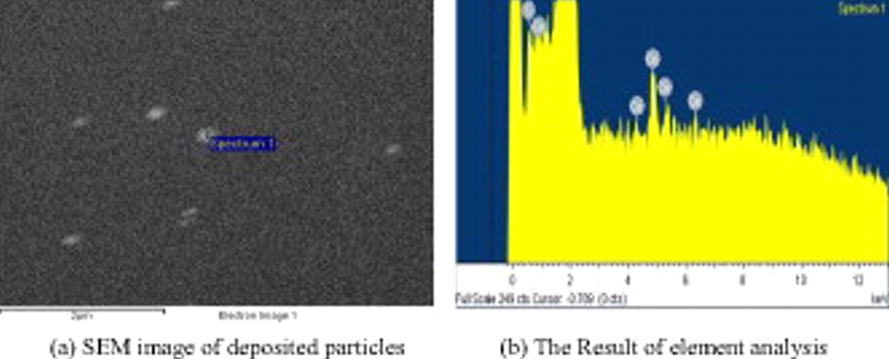
Figure 4. Analysis result of deposited particle element using SEM/EDX.
The amount of abrasives deposited on the silicon wafer as a function of deposition time is shown in Fig. 5a, and the DRAM-patterned wafer is shown in Fig. 5b. The number of deposited abrasives increases as the deposition time increases from 30 min to 4 h. The deposition time was defined by the time taken to deposit the same number of ceria particles on each wafer. The deposition time for the abrasive of 100 nm that has approximately 7000 particle counts/mL was 4 h. In the 30 nm abrasive that has approximately 3000 particle counts/mL, the deposition time was determined to be about 9 h. Also, the deposition times of the abrasives of other sizes were determined in the same manner. In the abrasives of 400 and 500 nm, it took too long to deposit the same number of particles because of the small amount of abrasive in the slurry. So, no polishing sample was made for those sizes. Figure 5b shows the defect map on the pattern wafers. The red dots on the scanning map indicate the deposited ceria abrasives. After 2 h of deposition with the 100 nm abrasive, the scanning system was overloaded by the number of deposited particles, so the entire surface of the wafer could not be scanned. Therefore, we confirmed that the MDAD system can control the amount of abrasive deposition on a wafer qualitatively and quantitatively.
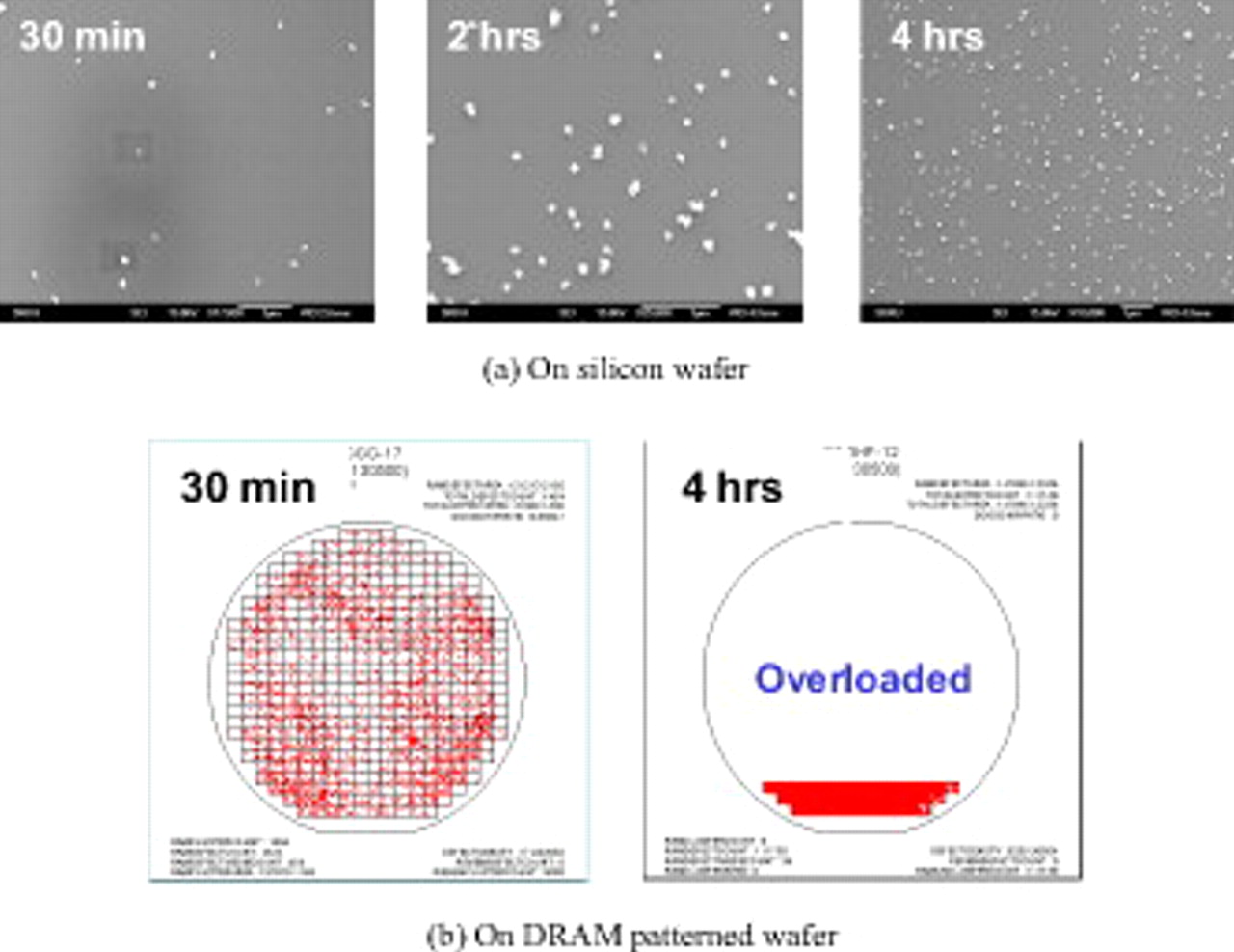
Figure 5. Abrasive deposition images of (a) silicon wafer and (b) patterned wafer according to the increase in deposition time.
The effect of the monodisperse abrasive size on the surface topography of the polished specimen is shown in Fig. 6. From the AFM data, an increase in the abrasive size can clearly increase the surface roughness. The surface roughness ranges from 1.5 to 3.4 nm. The surface roughness appears to be proportional to  , where
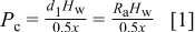
  is the abrasive size. The exponent in the regression curve showed that none of the suggested models in the other researches satisfactorily described the observed data for this study.8 This might be caused by the polishing characteristics of the different abrasives. The indentation depth into silicon could be estimated with the final surface roughness of the polished wafer. Once the measured roughness of the polished wafer and the accurate sizes of the active abrasives are known, the contact pressure and the ratio of the contact area can be calculated easily. Based on the fully plastic deformation and the abrasive indentation assumption, the contact pressure
  and ratio of the contact area
  can be derived as follows20
and
where  is the size of the active abrasives,
  is the mean cutting depth,
  is the wafer hardness,
  is the surface roughness measured by AFM, and
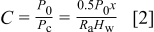
  is the down-pressure. Figure 7 shows the calculation results of the contact area ratio with experimental values and this model. The ratio of the contact areas between the pad and the wafer was from
  to
to  . Experimental results from Zhang et al. showed that the ratio of the contact areas was about
  at 3 psi.21 Tat-Kwan et al. also showed that the ratio lay between
  and
and  at 3 psi.22 The ratio of the contact areas in this experiment was 1 or 2 orders higher in magnitude. The higher ratio of the contact area may be explained from two viewpoints. Generally, the ratio of the contact area is estimated by comparing two areas that only consider the contact between the pad and the wafer. However, the result in this work is calculated by considering the contact between the wafer and the abrasives using the indentation modeling, which results in the smaller ratio of the contact area. Also, this might be due to the difference in the polishing mechanism between the silica abrasive and the ceria abrasive. Generally, ceria abrasives have a higher removal rate than silica abrasives for blanket wafers. This difference may be due to the chemical tooth mechanism of the ceria polishing. Ceria removes larger amounts of material from substrates with large activation sites.23, 24 This suggests that the ceria abrasive has a higher removal rate per unit contact area than silica abrasives.
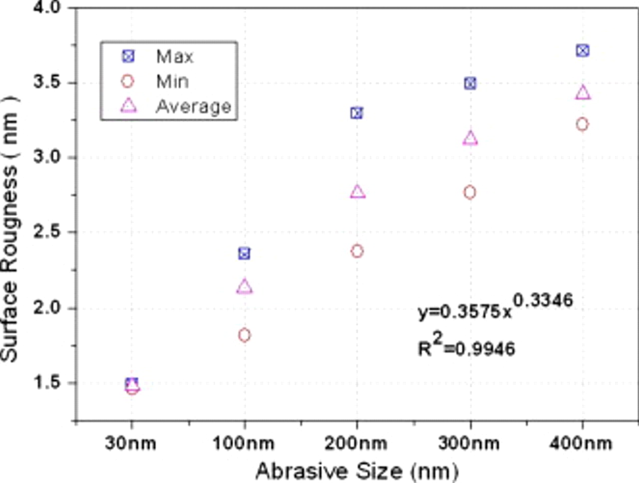
Figure 6. Result of surface roughness for various abrasive sizes.
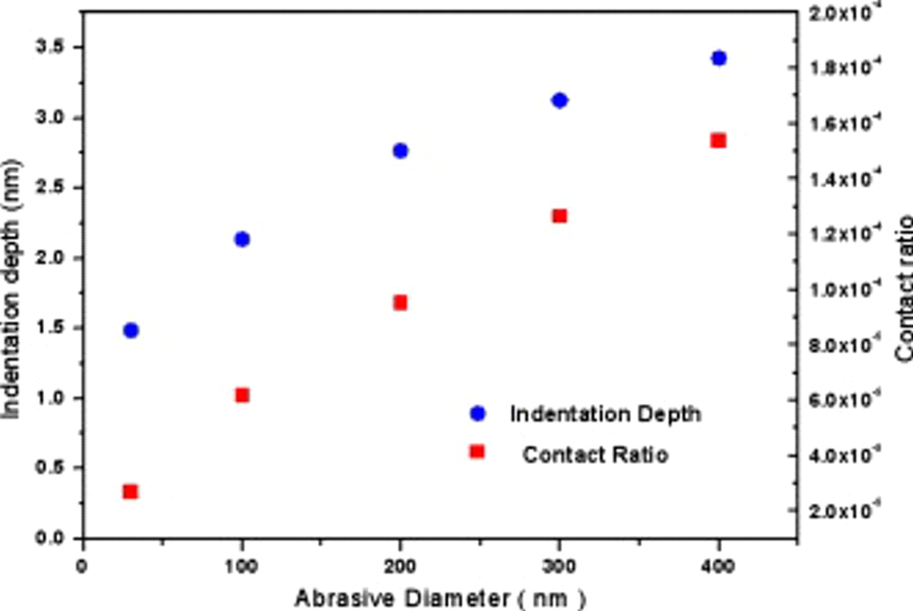
Figure 7. Calculation results of contact area with fully plastic contact modeling.
To explore the details of the microstructural changes and atomic bonding configurations of the material, high resolution transmission electron microscopy (HRTEM) was used to observe the variation of the surface layer after CMP, as shown in Fig. 8, where each dot indicates a silicon atom. A deformed layer, which is characterized by the reduced lattice distance between silicon atoms, generated by polishing was shown in the TEM images. The average thickness of each deformed layer increased with the increase in the ceria abrasive size. There was little subsurface damage in the polished wafer with the 30 nm ceria abrasive. In the 100 and 200 nm ceria abrasive, three to four layers and five to six layers of silicon lattice were deformed into the surface, respectively. There was no sign of an amorphous layer until the 200 nm ceria abrasive. But a TEM image of the wafer polished with the 300 nm ceria abrasive showed a severely deformed amorphous layer on the subsurface. Note that the structure of the material inside the damaged layer changed with the ceria abrasive size. Especially, the structure of the deformed layer resulting from the use of the 300 nm ceria abrasive distinctly differed from that resulting from any other size of the ceria abrasive, where the crystalline structure can be sustained. (Fig. 7a, 7b and 7c) The subsurface damage induced by the polishing pressure was also reported,25 and the amorphous phase transformation occurred with all pressure conditions over 3.6 psi for an average particle size of 40 nm. The test results for the 3 psi pressure condition showed a much smaller and uniformly damaged layer. The observed decrease in the deformed layer could have been caused by the absence of chemical effects in the experimental condition of the mechanical DI polishing. In addition, it is thought that the uniformly damaged layer was induced by the use of the monodisperse abrasive size. The silicon wafers polished with monosized ceria abrasives were also checked with respect to surface damage by a wafer surface inspection system with resolution of 40 nm. Figure 9 shows the magnitudes of the surface topography and scratches as a function of the ceria abrasive size. To enlarge the surface roughness and defects, the wafers were treated by 0.2% diluted HF-assisted brush scrubbing for 120 s. A conformal etch process such as a wet etch using diluted HF can enlarge the small surface roughness and makes it visible under defect inspection tools. As shown in Fig. 9, a more damaged surface was observed on the wafer polished with larger abrasive sizes. It is speculated that the topography generated may be due to the difference in the contact areas between the wafer and the abrasives. The contact area and volume removed by a single abrasive are dependent on the abrasive size through the indentation depth. Also, when the structural deformation induced by the ceria abrasive becomes high enough, nanodislocation on the silicon surface occurs, as shown in Fig. 8. A surface inspection system has revealed that a diluted HF process removes some of the broken materials as well.26 However, line scratches were observed on all sizes of abrasives. This phenomenon does not agree with the conventional scratch mechanism, in which microscratches are usually caused by the larger particles. The scratches on the polished surface with ceria abrasives, which is characterized by higher density, hardness, and a more angular morphology, depend not only on the abrasive size, but also on the contact condition between the pad and the wafer.
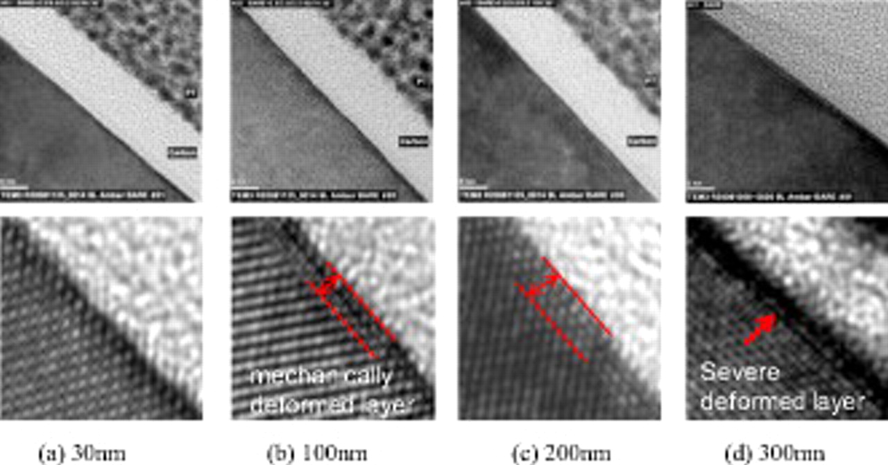
Figure 8. Cross section HRTEM images of the polished surface according to abrasive sizes.
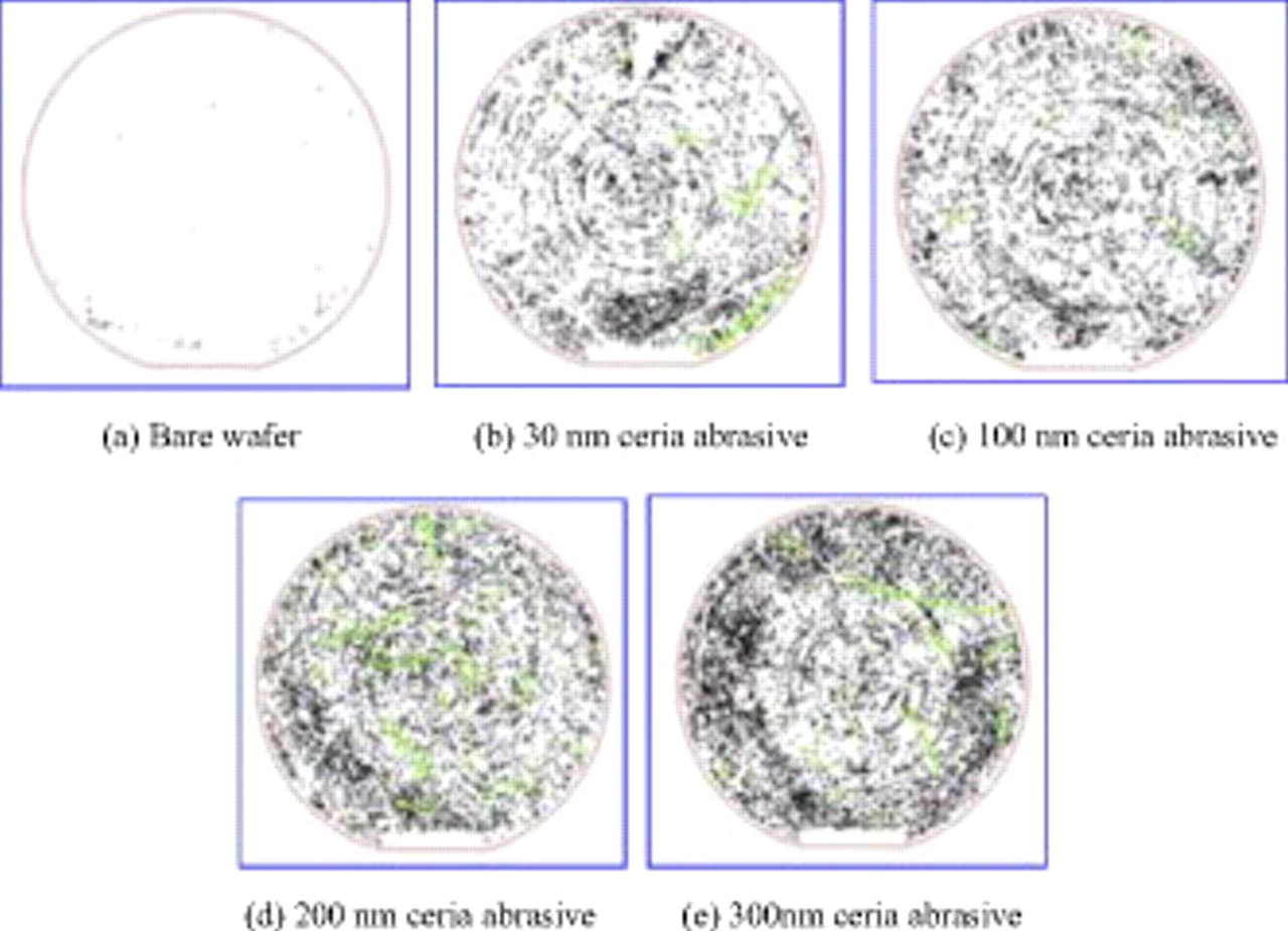
Figure 9. Result of wafer surface inspection according to abrasive sizes.
The polishing effects of different abrasive shapes and morphologies in the same abrasive diameter were investigated for three kinds of abrasives by the MDAD system. Even though the abrasives are of the same size in terms of the diameter, the dissimilar density and surface morphology, which could be attributed to the fabrication process of the abrasives, can change the surface integrity of the polished wafer surface. Figure 10 shows the result of the surface roughness measured by AFM and the images of the subsurface damage by TEM. TEM specimens were also treated with diluted HF for 120 s to enlarge their surface defects. It was observed that the amount of surface damage was distinctly different even for the same 200 nm abrasive size. The surface integrity shown in the TEM images fairly agreed with the surface roughness obtained from AFM. According to the contact mechanism, the material removal rate that can be modeled by the surface roughness is proportional to the abrasive density. Two types of abrasive densities related to the surface roughness can be considered in the CMP process. One is the unit volume density defined by the crystal structure, and the other is the bulk density, which can be calculated based on the open surface pore and voids. It has been established that the abrasive particle density could be used to characterize the hardness of submicrometer abrasive particles based on the material removal rates.26 Therefore, the crystal structure of the three abrasives was examined with X-ray diffraction (XRD). Because the same cubic crystal structure of  was found in all samples, it is concluded that all abrasives had the same unit density. Table I summarizes the crystal size of each ceria abrasive. All slurries have different crystal sizes from 14.2 to 32.5 nm. Therefore, there seemed to be no relationship between the crystal structures in terms of the unit density and surface roughness. But in the surface morphology, while the A- and C-type abrasives are an agglomerated type that produces many surface pores and voids on the surface, the B-type abrasive has one type of particle. From this, it is inferred that the agglomerated type of abrasive with a small contact area caused by surface pores and voids is superior to the particle type of abrasive with a large contact area with respect to the surface roughness and defect generation.
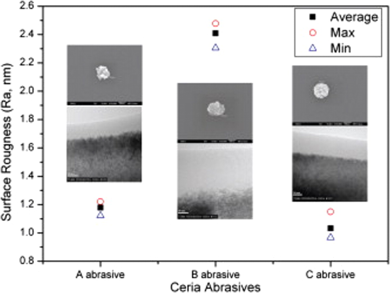
Figure 10. Result of surface analysis of polished wafer with three different 200 nm ceria abrasives.
Table I. Results of the XRD analysis of three types of abrasives.
| Sample | Full width at half-maximum (°) | B (rad) |

| θ | Radian | cos
| Crystal size (nm) |
|---|---|---|---|---|---|---|---|
| A abrasive | 0.2800 | 0.0049 | 28.5300 | 14.2650 | 0.2488 | 0.9692 | 32.5 |
| B abrasive | 0.31 | 0.01 | 28.55 | 14.275 | 0.25 | 0.97 | 29 |
| C abrasive | 0.6400 | 0.0112 | 28.5400 | 14.2700 | 0.2489 | 0.9692 | 14.2 |
Yoon et al. introduced the loading effect of the ceria slurry.27 They compared the removal rate of the silica slurry at the initial time of CMP and that of the ceria slurry for an STI-patterned wafer. In this study, the fundamental mechanism of this phenomenon was investigated by using the monosize abrasive. The STI and high aspect ratio patterned wafers were used to examine the loading effect, which denotes the low removal rate at the initial polishing time, according to the ceria abrasive size. Each patterned wafer was deposited with 100, 200, and 300 nm ceria abrasives. Figure 11a shows the removal shape at the top area of the STI structure as a function of the ceria abrasive size. The result showed that the increase in the abrasive size led to an increase in the removal amount of the top of the active area. A higher removal rate by a larger size abrasive observed in this study suggested that large particles could easily jump over and slide the step height barrier between trench areas, as shown in Fig. 11a. Figure 11b shows a pattern removal shape of the high aspect ratio pattern. In the same polishing time, a larger abrasive gave a higher removal rate. This phenomenon can be explained by the increase in the indentation depth with a larger abrasive on the pattern top area during polishing, according to an indentation-based mechanism.28 Based on the two experimental results, it was assumed that the low removal rate of ceria at the initial time for a patterned wafer was induced by lower moving efficiency and indentation depth resulting from the small size of the ceria slurry used. Therefore, a larger ceria abrasive is more effective in removing the initial pattern loading effects.
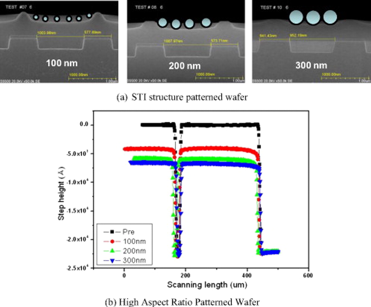
Figure 11. Material removal rate of (a) STI structure and (b) high aspect ratio patterned wafer as a function of ceria abrasive size.
Conclusions
In this study, the polishing characteristics of the monosized ceria abrasive were investigated by the developed MDAD system. The results of AFM measurements demonstrated that an increase in the abrasive size can increase the surface roughness of the polished wafer. From surface roughness data and precise abrasive size, the ratio of the contact areas ranged from  to
to  for the ceria abrasives. The defect generation mechanism of ceria abrasive was elucidated via TEM measurement and surface inspection system. Wafers polished with larger ceria abrasives showed more damaged surface. It was confirmed that the contact condition between the pad and the wafer is another important factor for controlling surface defects. It was also observed that the modification of the contact condition due to the change in surface morphology of the abrasive itself influenced surface defect generation. In the experiment, the agglomerated type of ceria was observed to be effective in reducing surface defects. In the pattern loading test, we concluded that a larger ceria abrasive, which has larger indentation depth, would be needed to alleviate the issue of low removal rates at initial polishing.
Acknowledgments
The authors thank Techno Semichem Co. and Jeil Industry for supplying the abrasives and for numerous insightful discussions.
Sungkyunkwan University assisted in meeting the publication costs of this article.