
Abstract
Nanoindentation was performed on Ti-B-Si-C and SiCN films deposited on Si substrates at varying loads and depths of penetrations. The intensity of chipping got enhanced with an increasing load which was represented geometrically. The pop-in and pop-out events occurring in the load and unloading were explained as cracking and high-pressure phase transformation. The interfacial fracture stability and adhesion of the film-substrate system, crucial for N/MEMS devices were analyzed with respect to frictional coefficient with the help of Finite Element Modelling (FEM).
Export citation and abstract BibTeX RIS
1. Introduction
The modern devices in today's world are based on nano/micro electromechanical systems (N/MEMS) and are mainly fabricated on silicon substrates [1–3]. Hard thin films having conductive, as well as piezoelectric properties, are an integral part of these systems. Materials like single/polycrystal silicon, SiN, SiC, and diamond-like tetrahedral amorphous carbon (ta-C) are used in the fabrication process. These materials possess high stiffness, thermal stability, and resistance to environmental conditions. Polymeric materials are used in conjunction with these materials to provide flexibility. SiCN and TiBSiC are composite coatings which contain a mixture of phases like SiC, SiNx, CNx, TiN, TiC , TiB2 etc which have individual technological importance in terms of metallurgical protection, corrosion and wear resistance and find applications fabricating interconnects and nano/microscale electro mechanical systems. A phase change occurring in these materials with a variety of fabrication parameters involving an interplay between nanocrystalline and amorphous phases is utilized in switching devices [4]. They have been studied extensively and structure-property correlations have been established previously [5–7].
The thin films used in MEMS need to have good thermal stability at high temperatures especially the ones used in piezoresistive sensors. Apart from good hardness, modulus, and adhesion, the film needs to have good fracture resistance. For the last few years, several attempts have been taken by different researchers to study the fracture properties of thin-film by correlating the Nanoindentation of the thin film with finite element analysis [8–12]. They approach to understand the failure mechanism happening in the film due to indentation in different ways. Jixi Deng et al [13] used the extended finite element analysis to predict the failure mechanism in the penetration region. The crack propagation path is an assumption in the model. In fracture mechanics, pre-cracking is done in the specimen to allow crack propagation in that specific region only. But in Nanoindentation, no pre-cracking is done in the specimen therefore defining the crack propagation path does not hold a holistic approach to address the problem. Some researchers like Yangyi Xiao et al [14] used the cohesive model to define the fracture phenomenon in the indentation region. Here also the definition of the crack path is needed but as per Nanoindentation is concerned. The different crack modes viz. radial—median, radial-Palmqvist, and Lateral are possible in the indented specimen. The stress distribution is however different when using a Berkovich nano-indenter [15, 16].
The crack propagation direction under indentation load cannot be predetermined. Assuming the crack path direction did not appear to the author a holistic approach to address the fracture definition in the indented material. Cohesive zone approach to the Pre crack specimen such as Compact Tension Specimen and Three-Point Bending Specimen can be more logical for finite element approach as done by S. Choudhury et al [17]. The problem has also been addressed based on Fracture Process Zone (FPZ). FPZ indicates the zone in the Brittle material where the Maximum Principal Stress exceeds twice the Yield stress of the material [18–20].
The area which needs a bit more study however is the adhesion of these films with the underlying substrate which is silicon in most cases. This is mainly because the conjunction between the film and substrate significantly affects the performance of the device. A recently published article has focused on this area using sliding indentation or scratch test [21]. However, when it comes to real-time testing, nanoindentation is the most reliable technique for lower dimensions.
Nanoindentation is based upon depth-sensing indentation, the mechanism of which has been mentioned in numerous reports [22, 23]. It involves indentation with increasing load using a three-sided pyramidal Berkovich indenter. The indentation load and displacement are recorded as shown schematically and experimentally in figure 1(a) where hr, he, ht, h.c. and ha are the residual elastic total contact depth and sink in depth respectively [23].

Figure 1. (a) Nanoindentation Load-depth (P-h) plot showing the different depth parameters [24] (b) Pile-up and sink-in and (c) Actual and corner to corner area during indentation pile up [25].
Download figure:
Standard image High-resolution imagePile up is observed for softer coatings on harder subjects like metals Al, Cu and Au deposited on Si which has a lot of technological importance especially in semiconductor industry. The amount of pile up occurring is again measured through ratio of corner area and actual contact area of the indenter impression (Aactual/Acc) as depicted in figures 1(b) and (c) [25].
Apart from having the suitable hardness and modulus, the fracture toughness and more importantly, the interfacial fracture toughness of the film-substrate system is important for the longevity of the devices [26], which again makes nanoindentation the preferred choice. As micro-machining is an integral part of MEMS fabrication. Hence the different microstructure, internal and residual stress and defects associated with the film/substrate system affect the overall mechanical behavior and the performance of the device [27]. The stress distribution and the contact mechanics involved in the indentation process have been studied with the help of Finite Element Modelling for other systems [27].
In this communication, we have focused mainly on the interfacial zone of the film/substrate system and tried to throw some light on the film failure mechanisms. The results of these studies will add to the knowledge in applying hard films for electro-mechanical device fabrications at the micro/nanoscale
2. Methods
Deposition of SiCN and TiBSiC coatings deposited on silicon substrates by magnetron sputtering was performed using a sintered SiC and TiBSiC target. The details of the deposition process along with structure-property correlations of these films have been published previously. Nanoindentation studies were performed on the films by Nanoindenter XP (MTS, USA) [6, 7].
FEM simulations were done using ABAQUS to study the stress distribution during the indentation causing delamination and fracture. In this work due to the axial symmetry of the specimen and the indenter, the model is simulated in axis-symmetric 2D condition. The Nanoindentation is done by axis-symmetric discrete rigid element with the half-included tip angle, of 70.3°. The thin film and substrate materials were represented by four nodes of axisymmetric CAX4R elements [28]. As the prediction of accurate simulation results demands the finer mesh size of the element used for analysis therefore a total of 68764 elements were used for 150X150 nanometer length of each side for the model shown in figure 2(a).

Figure 2. (a): Finite Element Mesh model (b) Force versus displacement curve resulted from the Finite Element Simulation.
Download figure:
Standard image High-resolution imageContact analysis is done on the regions of the model firstly between the rigid indenter and the thin film and secondly between the film and the substrate. In the first case surface to surface, contact is established where the rigid indenter surface is taken as the master surface and the thin film surface is taken as the slave surface and Normal behavior with hard contact is provided as the contact property. In the second case, the film surface is taken as the master surface and the substrate surface is taken as the slave surface. Tangential behavior with different coefficients of friction is provided as contact properties for different simulations done in this work. The analysis is performed in two steps. In Step1: Load is given in the form of displacement of 1000 nm in small incremental steps of maximum 1/100 to minimum 1/100000 of the given displacement, through the rigid indenter. In the Second Step Elastic recovery is modeled by withdrawing the indenter up to a depth of 800 nm as shown in figure 2(a). The load-depth plot obtained from FEM is shown in figure 2(b). A max load (Pmax) of 300 mN and a corresponding max load of 100 nm (hmax) can be observed. The unloading portion is used to determine the stiffness (S = dP/dh) which is further used indetermination of elastic modulus. The contact depth (hc) is used to find the projected area A = 24.5 hc 2 used in hardness determination [22, 23]. In real experimental data, the contact depth is always more than the residual depth due to the hysteresis effect.
3. Results and discussions
3.1. Nanoindentation fracture
Nanoindentations were performed for 500 nm to 2000 nm penetration depths and caused film failure by the formation of radial cracks, lateral cracks, crack branching, deamination, and chipping as can be seen in the optical images figures 3(a)–(e). The mechanism behind these events has been reported in detail previously [29, 30]. On increasing the load or depth of penetration, chipping can be first observed for 1000 nm (figure 3(b)) depth which further got larger for 1200 nm (figure 3(c)) and 1500nm (figure 3(d)) depth. The film failure got intensified further at 2000 nm depth with chipping occurring from the other side of the indenter impression as well (figure 3(e)).
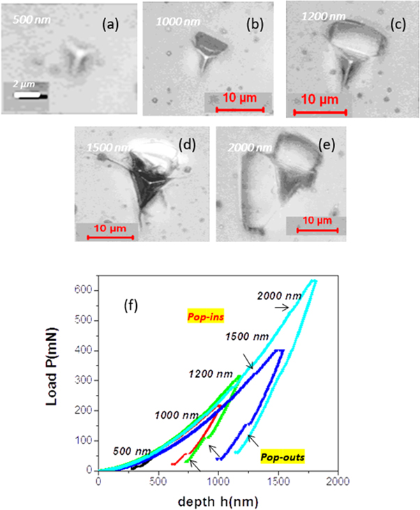
Figure 3. Nanoindentation of Ti-B-Si-C/Si at different (a) 500 (b) 1000 (c) 1200 (d)1500 (e) 2000 nm and the (f) corresponding load-depth (P-h) curves [29].
Download figure:
Standard image High-resolution imageThe corresponding load-depth (P-h) plots for depth of penetration are given in figure 3(f). The non-collinearity of the plots was due to the tip positioning as explained in ref [31]. The fracture phenomena during the indentation for 500 and 1500 nm depth of penetration have been previously analyzed based on the stress-strain plots and a new approach with shape factors in the fracture studies based on radial crack branching and micro-cracking has also been proposed [29].
The discontinuities shown by arrows in the loading portion are the pop-in events and indicate cracking which mainly occurs at higher loads (depth of penetration) as observed for 1500 nm and twice in 2000 nm penetration. The cracking phenomenon may occur in the case of lower penetration depths and may not be prominently visible in the load-depth plots. A derivative of the P-h i.e. dP/dh versus h may, however, indicate the cracking phenomena occurring [29]. The unloading portion indicates pop-outs due to the high-pressure phase transformation of the silicon substrate [32]. Interestingly, no pop-outs were observed for the 2000 nm depth of penetration plot which is because higher loading reduces the probability of nucleation of high-pressure phases below the indenter. The pop-in and especially the pop-out are due to phase change of Si with formation of Si-II from diamond cubic Si-I in the case of loading giving pop-ins. For the unloading part, the Si-II phase formed gets converted into Si-III/Si-XII for slower unloading which may get observed as feeble pop-outs for no discontinuity at all. For a faster rate of unloading however, a disordered crystalline of amorphous Si phase gets formed showing clear and distinct pop-out called an elbow [33].
Apart from Si phase transformation, minor Pop-in occuring during load mainly indicates picture frame cracking which is a type of cohesive failure [34]. Radial cracks occurring from the indentation corners are due to penny-shaped cracks if observed cross sectionally and are associated with coating strength or fracture toughness. The lateral cracks on the other hand are associated with film adhesion and occurs during unloading and may show minor pop-outs as well. These discontinuities in the P-h plot however get prominent when a stress-strain plot is derived out of them [29].
A P-h plot for SiCN/ Si film is shown in figure 4. The linear unloading indicated by the circle in the unloading portion of the curve is due to coating detachment beneath the indenter and as a result pushing the indenter [34]. Stress-strain plots and details regarding SiCN film failure can be found in details in ref [29]. The pop-in events in the load depth curve (shown by arrows) indicates the through thickness picture frame fracture (inset) of the hard coating during indentation [30, 34]. The probability distribution of the pop-in events was plotted with respect to contact stress drop Δσ which is defined by the relation given in equation (1) where P' corresponds to the load at which pop-in occurs for the depth h and h + Δh; A (h) and A (h + Δh) are the corresponding indenter contact areas [35]. The probability distribution of the contact stress rises to maximum at a certain load and then showed a decrease at higher loads indicating mixed mode failure with brittle failure dominant initially causing an increase in Log Δσ value followed by ductile (plastic deformation) failure.


Figure 4. Load-depth (P-h) curves during Nanoindentation of Si-C-N/Si (b) Probability distribution involving contact stress at the pop-in events depicting mixed mode film failure.
Download figure:
Standard image High-resolution imageThe stress field generated beneath the 3sided Berkovich indenter leads to cohesive and adhesive failure of the film which gets reflected as delamination and spallation as shown in figure 5. The first stage of adhesive failure is when the coating starts to get detached from the substrate (Buckling) followed by full detachment (spallation) which may also cause chipping of the film components in the case of high brittleness. All these phenomena are observed as fracture surrounding the indenter impression as shown below [30]. The chipping occurs from one of the indentation sides initially and all sides with higher loads are used in toughness calculations as shown in figure 6(a) [29, 34, 36]. Increasing the load leads to chipping from other sides as well as shown in figures 6(b)–(d).

Figure 5. Film adhesive and cohesive failure by nanoindentation [30].
Download figure:
Standard image High-resolution image
Figure 6. (a) Chipped segment geometry to calculate interfacial toughness [29] (b)–(d) chipping occurring from other sides of the indenter for further penetration.
Download figure:
Standard image High-resolution image3.2. Finite element modelling
The objective of this communication was to study the role of interface in fracture and hence the coefficient of friction (μ) was varied to study the role played by contact mechanics by FEM (figure 7). The values of μ taken where 0.01, 0.02 and 0.08. Two depths of penetration (500 nm and 1000 nm) were considered in each case to see the effect of indenter penetration. The stress distribution can bee seen as the indenter starts to penetrate the substarte. What is interesting to see is there are two separate stress distribution for the two different layers above and below the interface and the delamination is caused by not joining of these two regions causing the film to start getting detached from the substrate (delamination) followed by adhesive failure (spallation) as shown earlier in figure 5. The difference in joining of the stresses between the film and the substrate is represent by the double-sided arrow. The region just beneath the indentation corresponds to the enclave of residual compressive pulse which occurs as the plastic zone grows in size due to overload and is unable to regain its shape Indentation causes shear stress which acts in the slip plane containing the dislocation. The dislocation bulges out and produces a slip and annihilation to form a large loop (indicated as 1) for 500 nm penetration, and also a new source of dislocation which forms a smaller loop inside (indicated as 2) on increasing the penetration depth to 1000 nm (figures 7(a), (b)). The second loop is pretty much inside the first loop maintaining the appreciable distance from the interface, The adhesive spallation was also more for 1000 nm penetration. The plastic zone is as per Von-Mises yield criterion and take the shape of a cardioid [15].

Download figure:
Standard image High-resolution image
Figure 7. FEM simulation of stress distribution during nanoindentation with different coefficient of friction and indentation depths (a) μ = 0.01, 500 nm (b) μ = 0.01, 1000 nm (c) μ = 0.02, 500 nm (d) μ = 0.02, 1000 nm (e) μ = 0.08, 500 nm (f) μ = 0.08, 1000 nm.
Download figure:
Standard image High-resolution image
It was observed that an increase in COF caused flattening of the plastic zone beneath the indentation, an early arrival of the new dislocation loops and reduction in the intensity of adhesive failure (figures 7(c), (d)). For higher COF, not only there is the generation of more new dislocation sources forming loops (region 3) but they also expand out and meet the ones coming from the film at the interface (figures 7(e), (f)). As the plastic one is surrounded by a rigid elastic region, the slip lines extend along the interface causing flattening of the plastic zone for higher COF.
A new parameter called interfacial shear fracture stress can be introduced because the indentation force gets countered by opposing restoring force from the substrates causing film delamination (failure) at the interface. The mechanism is however completely different from the normal shear stress. It is the area of coverage that is important in this case rather than the magnitude of stress. In the low COF cases, the indentation stress distribution area is larger than the reaction force area, and hence delamination occurs. The annihilation of Franck Reed dislocations occurs at the interface for higher COF which also aid in the film failure. On increasing the COF, the reaction force coverage also increases and delamination is less. Thus, an increase friction at the interface causes more resistance towards adhesive film failure.
4. Conclusions
The chipping phenomenon during nanoindentation of TiBSiC films was qualitatively quantified with geometrical shapes. The pressure-induced transformation due to the silicon substrate was observed and higher indentation loads, which also negated the nucleation of high-temperature phases beneath the indentation region. The increase in coefficient of friction was found to be necessary for better resistance towards adhesive film failure.
The discussions presented in this communication provide practical experimental facts and a theoretical base for N/MEMS device fabrication involving hard thin films.
Acknowledgments
The author acknowledges Dr S K Mishra, National Metallurgical Laboratory Jamshedpur for the instrumental facilities. The authors would also like to thank Mrityunjay Prasad, Ashwini Kumari, and Pragya Singh for their help.
Data availability statement
The data that support the findings of this study are available upon reasonable request from the authors.
Ethics approval
The submitted work is original and has not been published elsewhere in any form or language.
Disclosure of potential conflicts of interest
There is no potential conflict of interest.
Research involving Human Participants and/or Animals: NA
Funding
The authors declare that no funds, grants, or other support were received during the preparation of this manuscript.
Competing interests
The authors have no relevant financial or non-financial interests to disclose.
Author contributions
All authors contributed to the study's conception and design. Material preparation, data collection, and analysis were performed by R. Dash, K. Bhattacharyya, R.P.Kumar and A.S. Bhattacharyya. The first draft of the manuscript was written by A.S. Bhattacharyya and all authors commented on previous versions of the manuscript. All authors read and approved the final manuscript.