
Abstract
The traditional von Neumann computing architecture has relatively-low information processing speed and high power consumption, making it difficult to meet the computing needs of artificial intelligence (AI). Neuromorphic computing systems, with massively parallel computing capability and low power consumption, have been considered as an ideal option for data storage and AI computing in the future. Memristor, as the fourth basic electronic component besides resistance, capacitance and inductance, is one of the most competitive candidates for neuromorphic computing systems benefiting from the simple structure, continuously adjustable conductivity state, ultra-low power consumption, high switching speed and compatibility with existing CMOS technology. The memristors with applying MXene-based hybrids have attracted significant attention in recent years. Here, we introduce the latest progress in the synthesis of MXene-based hybrids and summarize their potential applications in memristor devices and neuromorphological intelligence. We explore the development trend of memristors constructed by combining MXenes with other functional materials and emphatically discuss the potential mechanism of MXenes-based memristor devices. Finally, the future prospects and directions of MXene-based memristors are briefly described.
Highlights
The synthesis process of MXene and the application of MXene-based hybrids for memristors are summarized.
This article reviews the progress of MXene-based memristors in structural design, device performance, and applications in neuromorphic devices.
The article discusses the opportunities and challenges associated with developing memristors based on MXene materials.
Export citation and abstract BibTeX RIS

Original content from this work may be used under the terms of the Creative Commons Attribution 4.0 license. Any further distribution of this work must maintain attribution to the author(s) and the title of the work, journal citation and DOI.
1. Introduction
With the rapid development of internet of things, big data and artificial intelligence (AI), the current computing technology cannot meet the requirements of fast processing rate and low power consumption. Significantly, neuromorphic computing has been proposed to tackle those issues, benefiting from the strong capabilities in parallel computing [1–3]. Before the advent of memristor, there were three basic electronic components, namely resistor, capacitor, and inductor [4]. Currently, memristors have been acknowledged as highly promising candidate components in constructing neuromorphic computers, owing to their simple construction, smoothly variable conduction state, extremely low energy consumption, sufficiently high switching rate, and high compatibility with CMOS technology [5–11]. A memristor can be constructed using a certain resistive material as an insulator layer, which is connected with two metal electrodes to form a metal-insulator-metal architecture. Initially, oxide materials were employed in memristors; however, they exhibited relatively low switching characteristics and high power consumption in practical applications. Consequently, the development of new materials is imperative to enhance memristors for neuromorphic devices and computing applications [12].
Two-dimensional (2D) nanomaterials are likely to emerge as potential candidates for neuromorphic device applications due to their atomic-scale thickness, abundant surface information, and distinctive physical and chemical properties [13–17]. In contrast to those made of traditional metal oxides, memristors with 2D nanomaterials are strongly flexible and require less power [18–22]. Moreover, 2D nanomaterials could be stacked through molecular interaction to obtain properties beyond the pristine components [23–25]. As a new group of 2D nanomaterials, MXenes have been widely and extensively explored for new field applications [26–28]. Partially, MXenes-based memristors have become a hot research topic to date [15, 29–32].
In MXenes, Mn +1AXn has a typical hexagonal layer structure with two units, where the M layers are formed via inherent stacking of X. In this case, X occupies the octahedral site in the structure, whereas A is situated in the interlayer spaces of Mn +1Xn , providing special functionalities [33]. The M–X bonds could be ionic, covalent or metallic in the ways of bonding, thus leading to the presence of laminal configuration, and hence strong anisotropy. Moreover, MXenes exhibit high electrical conductivity due to the metallic behavior of the M–A bonds. Additionally, because the bonding strength between different layers of Mn +1AXn is strong, the exfoliation behavior of Mn +1AXn significantly differs from that of both graphite and transitional metallic dichalcogenide materials with relatively weak van der Waals bonds [34, 35]. The M–X bond and M–A bond also differ in bonding strength, with the A-layer being more active than the X-layer. As a consequence, Mn +1AXn can be readily exfoliated using suitable selective etching, resulting in the derivation of Mn +1Xn Tx MXenes with unique functionalities. Moreover, Tx represents surface-terminated functional groups such as oxygen (=O), hydroxyl (–OH), and fluorine (–F) that are introduced during the selective etching process and strongly attached onto the M items in the MXene phases. The thickness of the Mn +1Xn Tx MXene phases varies with different values of n, as the n value determines the size of the octahedral blocks. For example, when n = 1, 2 and 3, the octahedral blocks would have single-, double-, and triple-units, respectively.
The precursors of MXenes usually have a chemical formula of Mn +1AXn , in which the A atom is most likely to be aluminum (Al) that can be removed. Although it can be taken away by heating to achieve thermal etching, the layer structures could be damaged or destructed, leading to a complete loss of the layered nature as 2D materials [36]. Moreover, both M and A atoms could be eliminated from the parent compounds through chlorination reactions at sufficiently high temperatures, whereas the resulting products are porous structures instead of the desired layered constructions [37]. In other words, for fabricating MXenes with promising layer structures, it is necessary to employ chemical etching processes. For instance, the first reported MXene, Ti3C2, was prepared using HF solution as the etching agent to selectively remove Al atoms from Ti3AlC2. This process can be conducted at ambient conditions, specifically at room temperature [38]. In fact, the precursor compounds can also be nitrides, thus a general formula with a chemical composition of Mn +1AXn is used for the presentation [39]. Furthermore, Mn +1AXn could form solid solutions with more complicated chemical compositions, where different elements are located at the sites of M, A, and X, resulting in the formation of many more MXenes [40–42].
This article aimed to highlight the latest progress in the applications of MXenes as key materials for the construction of neuromorphic devices [43–48]. Firstly, the processing routes of MXene are introduced, including the development of synthetic processes, HF etching, fluoride salt etching, Lewis acidic molten salts etching, and direct chemical vapor deposition (CVD). The article also provides an overview of MXene-based memristor devices and their application in neuromorphological intelligence. Then, the memristors constructed with MXenes (either alone or in combination with other functional materials) are discussed, with a particular emphasis on understanding the potential mechanisms. Finally, future prospects and directions of MXene-based memristors for neuromorphic applications are briefly described.
2. Processing routes of MXene
2.1. Development of synthetic process
As mentioned above, 2D Ti3C2Tx MXene was initially produced using HF as the selective etching agent. Subsequently, various etching processes were explored. As a result, a wide variety of MXenes have been developed, each with its corresponding compositions. While several strategies have been developed, the fluoride-based agents are most-widely adopted for peeling 3D MXA phases. It is worth noting that different strategies can lead to different surface properties and functionalities, making it essential to have a comprehensive understanding of these synthetic methods.
Figure 1 illustrates various synthetic processes for the development of MXenes [49]. The HF etching method was the earliest strategy employed to synthesize MXenes [38]. Subsequently, a series of new methods have been developed for preparing MXenes, including dimethyl sulfoxide delaminating [50], bifluoride salts or HCl + LiF etching [51], Tetrabutylammonium hydroxide 30-hydrate intercalation [52], CVD [53], mechanical stripping [54], fluorine-based molten salt etching [55], electrochemical etching [56], concentrated alkali hydrothermal etching [57], fluorine-free molten salt etching [58], and Lewis acid molten salt etching [59]. Recently, innovative methods for preparing MXenes have been proposed, including microwave-assisted rapid MAX phase etching and delamination [60], high-temperature reaction synthesis [61], and chemical scissor-mediated structural editing method [62].
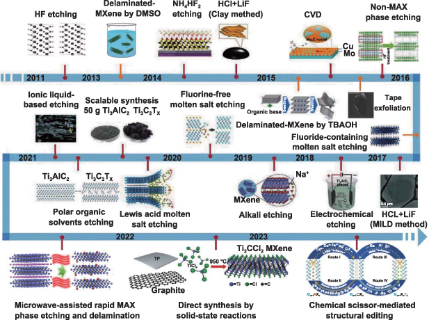
Figure 1. Timeline of the progress in MXene synthesis. Images for 2011–2021 year reproduced with permission from [49], Copyright © 2021, Wiley-VCH. Images for 'microwave-assisted rapid MAX phase etching and delamination' reproduced with permission from [60], Copyright © 2022, Elsevier. Images for 'high-temperature reaction synthesis' reproduced with permission from [61], images for 'chemical scissor–mediated structural editing' reproduced with permission from [62], Copyright © 2023, AAAS. [49] John Wiley & Sons. © 2021 Wiley‐VCH GmbH. Reprinted from [60], © 2022 Elsevier B.V. All rights reserved. From [61]. Reprinted with permission from AAAS. From [62]. Reprinted with permission from AAAS.
Download figure:
Standard image High-resolution imageIn general, both top‐down and bottom‐up strategies are employed to prepare 2D MXenes [63, 64]. In the top-down approach, few or even single-layer sheets of 2D MXenes are prepared by exfoliating bulk MAXs. On the other hand, in the bottom-up approach, 2D MXenes are grown from atoms [65, 66]. For instance, ultrathin 2D α‐Mo2C nanosheets, with sizes of 100 µm, were prepared using the CVD method, demonstrating superconducting properties [53]. Conversely, MXenes produced by bottom-up method often have relatively large sizes with minimal defects, while the top-down method involves the use of strong corrosive chemicals [38].
To achieve the top-down synthesis of MXenes, such as Ti3C2Tx , the precursor compound of Ti3AlC2 can be synthesized using the conventional solid-state reaction method. One approach is to use Ti2AlC and TiC as reactants, which react at sufficiently high temperatures to form Ti3AlC2. Various processing parameters, such as chemical purity of the starting powders, reaction duration, temperature and environment [50], can influence the chemical and physical behaviors of the precursor compounds. Numerous processing routes have been reported in the literature for developing Ti3C2Tx MXenes with different etching agents, such as HCl–LiF, NH4HF2, and NH4F [50, 67–69]. Representative synthesis methods and typical conditions for MXenes preparation are listed in table 1, along with their advantages and disadvantages.
Table 1. Representative synthesis methods for MXenes.
| Representative cases | |||||||
|---|---|---|---|---|---|---|---|
| Methods | Advantages | Disadvantages | MXenes | Precursors | Etchants | Etching conditions | References |
| HF etching methods | High efficiency, suitable for the preparation of most MXenes | HF has severe corrosiveness and poses risks for operation | Ti3C2Tx | Ti3AlC2 | 50 wt% HF | RT, 2 h | [38] |
| Nb2CTx | Nb2AlC | 50 wt% HF | 55 °C, 40 h | [70] | |||
| Ti3CNTx | Ti3AlCN | 30 wt% HF | RT, 18 h | [71] | |||
| (Nb,Ti)4C3Tx | (Nb,Ti)4AlC3 | 50 wt% HF | 50 °C, 96 h | [51] | |||
| Ti3C2Tx | Ti3SiC2 | 30 wt% HF/35 wt% H2O2 | 40 °C, 45 h | [72] | |||
| In situ HF formation etching | Reduced corrosiveness and operational risk | The fluoride-used agent is generally toxic | Ti2CTx | Ti2AlC | 6 M LiF + 0.9 M HCl | 40 °C, 15 h | [73] |
| Ti3C2Tx | Ti3AlC2 | 1 M NaHF2 | 60 °C, 24 h | [74] | |||
| Ti3CNTx | Ti3AlCN | 7.5 M LiF + 6 M HCl | 30 °C, 12 h | [75] | |||
| (Nb,Zr)4C3Tx | (Nb,Zr)4AlC3 | 2.3 M LiF + 12 M HCl | 50 °C, 168 h | [51] | |||
| Mo2CTx | Mo2Ga2C | 3 M LiF + 12 M HCl | 35 °C, 144 h | [76] | |||
| Alkali etching | Easy to obtain raw materials, low cost, and low operational risk | Require high reaction temperature and long reaction time | Ti3C2Tx | Ti3AlC2 | 1 M NaOH + 1 M H2SO4 | 80 °C, 100 h + 80 °C, 2 h | [77] |
| Ti3C2Tx | Ti3AlC2 | 27.5 M NaOH | 270 °C, 12 h | [57] | |||
| Ti3C2Tx | Ti3AlC2 | 125 M KOH | 180 °C, 24 h | [78] | |||
| Electrochemical etching | Easy to obtain raw materials, low cost, and low operational risk | Additional power supply needs to be introduced | Ti3C2Tx | Ti3AlC2 | 1 M NH4Cl+ 0.2 M TMAOH | 5 V, 5 h | [56] |
| Ti2CTx | Ti2AlC | 2 M HCl | 0.6 V, 120 h | [79] | |||
| V2CTx | V2AlC | 1 M HCl | 0.5 V, 9 h, 50 °C | [80] | |||
| Molten salt etching | Raw materials are less toxic and corrosive | Need high temperature and protective atmosphere | Ti2CTx | Ti2AlC | ZnCl2 | 550 °C, 5 h, Ar | [58] |
| Ti2CTx | Ti2GaC | CuCl2 | 650 °C, 24 h, Ar | [59] | |||
| Ti4N3Tx | Ti4AlN3 | KF + LiF + NaF | 550 °C, 0.5 h, Ar | [81] | |||
| Ta2CTx | Ta2AlC | AgCl | 700 °C, 24 h, Ar | [59] | |||
| Ti3CNTx | Ti3AlCN | CuCl2 | 700 °C, 24 h, Ar | [59] | |||
| Other etching methods | Raw materials are less toxic and corrosive | / | Ti3C2Tx | Ti3AlC2 | I2 | 100 °C | [82] |
| Mo2C | Mo2Ga2C | Ultraviolet light (100 W) | 3–5 h | [83] | |||
| Ti2CTx | Ti2SC | Thermal reduction strategy | 400–900 °C, 30 min, Ar/H2 | [84] | |||
| Ti3C2Tx | Ti3AlC2 | Algae | RT, 1 d | [85] | |||
2.2. HF etching route
Naguib et al fabricated the first example of layered Ti3C2Tx MXene derived from Ti3AlC2 powder through HF etching [38], with the preparation process and microstructure of the material shown in figure 2. When using HF solution as the etching agent, the A element is eliminated from the precursor compound by breaking the M–A bonds. The resulting MXene nanosheets can exhibit specific functionalization with simultaneous presence of –OH and –F surface terminal groups, which are introduced during the etching process, providing unique functional properties to the M layers [38]. Processing conditions, such as the concentration of the HF aqueous solution, temperature, and duration of the etching reaction [70, 71, 86], strongly influence the final product characteristics, including the types and concentration of defects, thickness and lateral size of the MXene phases, as well as the contents and species of the surface terminal groups. By employing these selective processes effectively, MXene phases with multiple layers and different compositions have been successfully obtained [51, 71, 87–89].
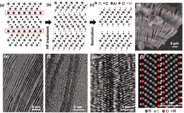
Figure 2. The preparation process and microstructure of Ti3AlC2: (a)–(c) schematic of the exfoliation process for Ti3AlC2 by HF etching route, (d) SEM image and (e)–(g) TEM images of the sample after HF treatment, (h) an atomistic model of the layer structure [38], Copyright © 2011, Wiley-VCH. [38] John Wiley & Sons. Copyright © 2011 WILEY‐VCH Verlag GmbH & Co. KGaA, Weinheim.
Download figure:
Standard image High-resolution image2.3. Fluoride salt etching route
Although the HF solution etching process has been successful in preparing Ti3C2Tx MXene, the toxicity of HF makes it unsuitable for industrial-scale applications [90–93]. Therefore, alternative etching agents with less toxicity and different compositions should be utilized. For example, mixtures of HF and fluorides (such as LiF) have been widely employed to remove Al from the precursor compounds [68]. In most cases, MXene phases obtained by HF solution etching have an interlayer distance (c-spacing) of around 20 Å. However, when a mixed solution of LiF/HCl is used, the resulting Ti3C2Tx MXene would have an interlayer spacing of up to 40 Å. This increased spacing can be attributed to the intercalation of H2O molecules or other cations within the interlayers of the Ti3C2Tx MXenes. Therefore, the use of LiF–HCl mixture etching solutions is promising in producing Ti3C2Tx nanoflakes with large lateral sizes and fewer defects. Additionally, this etching method can result in high productivity, approaching 100% [38, 71, 94]. Subsequently, various fluorides, such as NaF, KF, and NH4F, have been explored in combination with different acids as etching agents to obtain MXene phases [70, 95–97]. In this case, HF is generated through the chemical reaction between the fluoride compounds and the acids. Different cations, including Li+, K+, Na+, Al3+, NH4 + and Ca2+, can be applied for intercalating the Ti3C2 nanolayers. Furthermore, H2O molecules can also act as intercalators to expand the interlayer spacing. Overall, it has become feasible to develop MXenes with desired interlayer spacings and stronger adsorption behaviors [68, 69, 98].
Ti3C2Tx MXenes can also be fabricated in the form of thin films rather than powders. To achieve this, Ti3AlC2 films are firstly deposited on specific substrates, followed by the removal of Al atoms from the precursor [66]. This approach allows for the evaluation of various interesting properties of MXenes, including optical modulation characteristics, superconducting effects, magnetoresistance behavior, and conductivity capabilities. To achieve epitaxial deposition of the precursor films on the substrate, a thin layer of TiC is pre-coated as a buffer, resulting in Ti3C2Tx MXenes with strong atomic ordering. Moreover, the interlayer spacings of the MXene phases can be sufficiently expanded for special applications by intercalating both –NH3 and –NH4 + species with relatively large sizes into the nanosheets as functional groups.
2.4. Lewis acidic molten salts etching route
In 2019, Huang's group proposed a new strategy for synthesizing MXenes through 'isomorphic substitution' based on Lewis acid molten salts for the first time [58]. This method replaces the A-position main group elements in the conventional MAX phase with transition group elements, resulting in the synthesis of a series of new MAX phase structural materials. The etching action of Lewis acid molten salt enables M atoms to become coordination centers and interact with halogen anions in the molten salt, thus achieving MXene materials without the use of fluorinated etchants [59]. Figure 3 depicts a schematic illustration of the Ti3C2Tx MXene synthesis through the reaction of Ti3SiC2 with CuCl2 at 750 °C. The morphological and structural characterizations of Ti3C2Tx confirm its phase composition and layered structural characteristics. The Lewis acid molten salt synthesis method provides a novel approach for the preparation and structural regulation of MAX phase and MXene materials. However, due to the physical and chemical properties of conventional Lewis acid molten salts, the applicability of this method still has significant limitations.
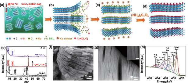
Figure 3. Schematic diagram of Ti3C2Tx MXene made with Lewis acidic molten salts etching route and structure characteristics of the MXenes: (a)–(d) the preparation process, (e) XRD patterns, (f) SEM image, (g) STEM image and (h) XPS spectra images of the obtained MXene [59], Copyright © 2022, Springer Nature. Reproduced from [59], Copyright © 2020, The Author(s), under exclusive licence to Springer Nature Limited.
Download figure:
Standard image High-resolution image2.5. Direct synthesis
In 2023, Talapin's group reported a method for directly synthesizing MXenes through a high-temperature solid-state reaction [61]. They ground Ti and graphit and then mixed them with TiCl4. The mixture was sealed in a quartz ampoule to be heated at 950 °C for 20 min. After the reaction was completed, Ti2CCl2 MXene was obtained. The high-temperature solid-state direct synthesis method opens up new opportunities for the preparation of high-performance MXene materials, especially when the corresponding MAX phase is unstable.
2.6. Other strategies
Various strategies have been reported for preparing MXenes. For instance, CVD processes can be utilized to deposit ultra-thin α-Mo2C MXene layers with large sizes and high crystallinity [53]. The produced α-Mo2C MXene films exhibit strong thermal stability in ambient environment, and thicknesses up to 0.1 mm. Magnetic field-aided studies have shown that α-Mo2C MXene films display unique anisotropic characteristics and superconductive behaviors. Interestingly, the superconducting effect is closely related to the film thickness. This process can also be extended to manufacture other materials. Clearly, this approach can be easily applied to other MXene phases as well.
3. Memristors based on MXenes
3.1. Ti3C2 MXene-based memristors
In 2020, Lu's group demonstrated the active layer of octylphosphonic (OP) acid-modified Ti3C2Tx MXene to construct memory devices with a stable ternary memory effect [99]. The device was constructed as a sandwich-layered memory structure with an 'Al/Ti3C2Tx -OP MXene layer/ITO glass' configuration (figure 4(a)). The Ti3C2Tx -OP MXene was spin-coated onto the ITO glass substrate at 1000 rpm, achieving an optimal thickness of 14 nm. The nonvolatile information memory of the Ti3C2Tx -OP MXene devices was attributed to charge trapping and filament conduction. Furthermore, a flexible Ti3C2Tx -OP memory device based on polyethylene terephthalate was assembled, exhibiting stable ternary memory performance even after bending for 5000 cycles.
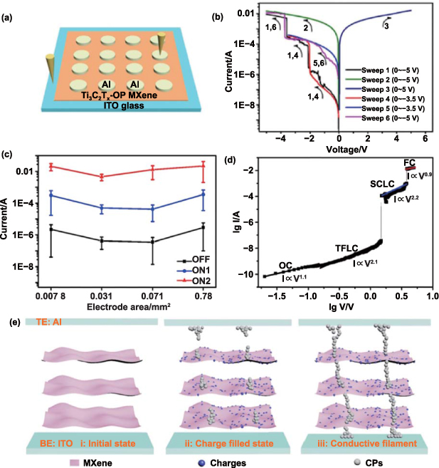
Figure 4. Ti3C2Tx -OP MXene memory device diagram and related electrical properties: (a) structure diagram of Ti3C2Tx -OP MXene-based memory, (b) current–voltage characteristics, (c) current level-electrode area, (d) lgI–lgV relationship curve of the Ti3C2Tx -OP MXene devices, (e) schematic diagram of the mechanism of the Ti3C2Tx -OP MXene memory device. Reprinted with permission from [99]. Copyright (2020) American Chemical Society.
Download figure:
Standard image High-resolution imageWhen a bias voltage ranging from 0 V to −5 V was applied to the device, current was observed at two specific voltages, −2.1 V and −3.7 V, during sweep 1 (figure 4(b)). Ternary memory states, namely '0' (high-resistance state), '1' (intermediate-resistance state), and '2' (low-resistance state), were achieved. Once the device was written to the '2' state, it could not be restored to the original state by positive or negative voltages (sweeps 2 and 3), resembling an information-writing process. Moreover, the '1' state (sweep 4) could be obtained by controlling the scan voltage (0 V to −3.5 V), and it was readable during sweep 5. During the second round of voltage scanning from 0 V to −5 V, the device could be restored from '1' state to '2' state (sweep 6). The three resistance states could be individually read at a low bias of −0.1 V, with no significant degradation observed for 4000 s.
The devices exhibited low threshold voltage, steady retention time, highly discernible resistance states, high ON/OFF rate (OFF/ON1/ON2 = 1: 102.7: 104.1), and significant ternary yield (58%). Additionally, the Ti3C2Tx -OP MXene memory displayed a nonlinear relationship between electrode area and current (figure 4(c)), suggesting the presence of conductive filaments. The lgI–lgV curve of the device is shown in figure 4(d). At low-bias voltages, charges were generated through thermal excitation, resulting in an I–V curve following Ohm's law, as illustrated in figure 4(e-i). As the bias voltage increased, charge traps were filled and approached the Fermi level, leading to a square law dependence (I∝ V2.1), known as the 'charge fill limiting current' [100]. At the first threshold voltage (Vth1), all charge traps were rapidly filled ('1'), leading to the formation of conductive filaments, as demonstrated in figure 4(e-ii). The I–V curve exhibited a square dependence (I∝ V2.2), known as Child's law, corresponding to the 'space charge-limited current phase'. Once the second threshold voltage (Vth2) was reached, the conductive filaments were established ('2'), resulting in the top and bottom electrodes being connected, as indicated the observed Ohmic behavior in figure 4(e-iii)[101]. The formation of the conductive filaments triggered the diffusion of aluminum ions [102]. Thus, the Ti3C2Tx -OP MXene exhibited the 'write once read many times' effect, while ON and OFF were not reversible.
Khot et al evaluated the potential of MXene in bipolar resistive switching (RS) and synaptic learning devices for digital and analog computing [103]. The authors focused on the performance of the Al/Ti3C2/Pt device exhibited superior RS and reliability compared to those with Ag and Pt top electrodes (figures 5(a)–(f)). In addition, the paper evaluates the enhancement and inhibition of biological synapses by measuring the memory resistance of the device (figures 5(g) and (h)). The results indicate that the Al/Ti3C2/Pt memristor device exhibits gradual changes in resistance during the enhancement and suppression processes, indicating that it is a good candidate for simulating advanced synaptic characteristics.

Figure 5. RS characteristics of devices in linear scales: (a) Ag/Ti3C2/Pt, (b) Pt/Ti3C2/Pt, and (c) Al/Ti3C2/Pt. VSET and VRESET distributions of memristors: (d) Ag/Ti3C2/Pt, (e) Pt/Ti3C2/Pt, and (f) Al/Ti3C2/Pt. (g) and (h) Potentiation and depression of synaptic properties of the Al/Ti3C2/Pt memristive device. Reprinted with permission from [103]. Copyright (2021) American Chemical Society. (i) Schematic illustration of integrate-and-fire in a biological neuron, and the leaky integrate-and-fire dynamics of Cu/Ti3C2/Cu memristors under a succession of pulses [104]. 24 January 2023, reprinted by permission of the publisher (Taylor & Francis Ltd, www.tandfonline.com.).
Download figure:
Standard image High-resolution imageIn 2019, a dynamics-driven artificial neuron device based on Cu/Ti3C2/Cu memristor was demonstrated. The electrical characteristics of the device could be well interpreted using the space-charge-limited current (SCLC) model combined with the electrochemical metallization effect [105]. The charge transport of the high conductance states was controlled by Ohmic law. The carrier transport behavior of low conductance states involved three stages: Ohmic conduction (I∝ V), Child's law (I∝ V2), and rapid current increment stage where the SCLC mechanism occurred. At positive voltage bias, Cu was oxidized and expelled from the top electrode, entering the MXene layer. The accumulation of Cu was accelerated after multiple voltage swept, leading to the formation of a filament that bridged the bottom and top electrodes. This filament resulted in a sharp increment in conductance. The conduction mechanism of this memristor can be used to simulate neural membrane dynamics. The Cu ions through MXene can play a role as biological transmitters in the ion channels of neurons. Similar to biological neuron, an artificial neuron receives input spikes to trigger an output action potential when the membrane potential reaches a threshold value (Vth), and the device can emulate biological integration and firing, as shown in figure 5(i).
In 2021, an Ag-nanoparticle doping strategy wasperformed to enhance the electrical properties of MXene Ti3C2-based memristor for neuromorphic behavior and decimal arithmetic operation applications [32]. The doping with Ag nanoparticles resulted in bidirectional continuous current transition behavior in the device. By analyzing the excitatory postsynaptic current (EPSC), a transition from short-term potentiation (STP) to long-term potentiation (LTP) was observed. The device also exhibited very low energy consumption. Importantly, with such memristor devices, decimal arithmetic operations, such as addition and multiplication, could be demonstrated. Microstructural and finite element analysis (FEA) results revealed that metal ions were captured by atomic vacancies, thus forming conduction filaments.
According to the high-resolution transmission electron microscopy (HRTEM) analysis of a typical Ti3C2 nanosheet (figure 6(a)), atomic vacancies were observed in the Ti3C2 nanosheet (yellow dotted line). Consequently, FEA was employed to simulate the resistance switching mechanism of the memristor device. The Ti3C2:Ag functional layer was considered as a 2D plane for energy analysis (figure 6(b)). Enlarging this area in figure 6(c) revealed that the energy was higher than that in other regions, suggesting that Ag ions could be attracted to the vacancies. Furthermore, current density around atomic vacancies, as observed in figure 6(d), was higher compared to other regions. Therefore, a strong driving force was generated to attract Al ions. The voltage distribution profile in the FEA simulation is shown in figure 6(f), indicating a uniform electric field. Additionally, figure 6(e) illustrates the process of capturing Ag ions by vacancies. Ultimately, metallic conductive filaments formed through the aggregation of metal ions.

Figure 6. Operation mechanism of the Al/Ti3C2:Ag/Pt memristor: (a) HRTEM of the Ti3C2 MXene nanosheet, with the atomic vacancy on the right side, simulated using Line profiles. (b) Energy distribution profile of the Ti3C2:Ag film. (c) Energy distribution profile of the atomic vacancy. (d) Current density distribution around the atomic vacancy. (e) Schematic diagram of Ag ions attracted by the atomic vacancy. (f) Voltage distribution of the stimulation. (g) Schematic diagrams of the formation of the Ag filaments. Reprinted from [32], © 2020 Elsevier Ltd. All rights reserved.
Download figure:
Standard image High-resolution imageSubsequently, a multifunctional optoelectronic hybrid-integrated neuron with Ag nanoparticle-doped MXene was developed to achieve optoelectronic spatiotemporal information integration [106]. This memristor exhibited exceptional performance with a low operating voltage of 0.93 V and a high ON/OFF ratio of 103. By integrating artificial synapses, artificial optoelectronic neurons, and robotic hands, visual perception systems could be constructed. The system's response time could be significantly reduced through the integration of optical sensory signals and electrical training signals. Moreover, with the capacity for spatiotemporal information integration, multi-task pattern recognition was achieved in the spiking neural network consisting of artificial synapses and neurons. As a result, digit patterns and rotation angles could be recognized.
3.2. V2C MXene-based memristors
In 2021, another memristor based on the V2C active layer with Ag and W electrodes was constructed [107]. The threshold-RS transition in the V2C-based memristor could be achieved by adjusting the compliance current. The switching mechanism was governed by the diffusion process of Ag+, similar to the dynamics of Ca2+ in synaptic transmission process. The V2C-based memristors, due to their positive analog behavior and the coexistence of threshold and RS mechanisms, could emulate various types of synaptic functions. Moreover, the V2C-based memristor allowed for spike-timing-dependent plasticity (STDP) and spike-rate-dependent plasticity (SRDP) through its intrinsic frequency-dependent characteristics, without requiring complex pulse engineering or spike overlapping. This reduced the complexity involved in circuit and algorithm design, enabling brain-inspired computing systems through simplified artificial synapse designs that improved efficiency and scalability.
It is well known that intracellular Ca2+ ions play a crucial role in stimulating changes in synaptic strength in biological neurons and synapses [108]. Figure 7(a) illustrates the dynamic balance between the concentrations of intracellular and extracellular Ca2+ near the pre-synaptic compartment. In this case, the concentration of Ca2+ is governed by the influxes through voltage-sensitive Ca2+ channels and N-methyl-d-aspartate receptors, as well as extrusion through the plasma membrane Ca2+-ATPase and the Na+/Ca2+ exchangers, which restore Ca2+ ions to baseline levels. The filamentary switching mechanism is depicted and schematically illustrated in the mode of threshold switching (TS) (figure 7(b)). The accumulation of Ag+ ions leads to an increase in current due to the external bias-driven migration of Ag+ ions. This mechanism is similar to the increment in synaptic potentials caused by the accumulation of Ca2+ ions through influxes via voltage-sensitive channels. Following this mechanism, the V2C-based memristor assumes that the Ag+ ions migrate to locations with the lowest energy when the electric pulse in TS mode is removed. This spontaneous return to an HRS with volatile characteristics resembles the maintenance of basal concentration of Ca2+ through extrusion mechanisms in biological systems. In other words, the V2C-based memristor in TS mode could emulate synaptic influx and extrusion of Ca2+, allowing for the emulation of increases and decreases in synaptic response potentials.
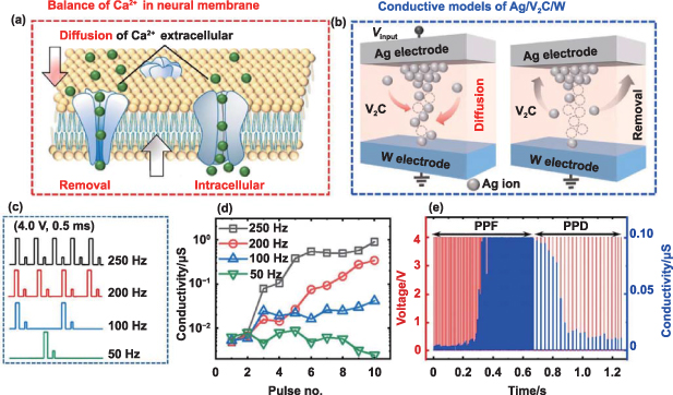
Figure 7. Emulation of synaptic Ca2+ transition and synaptic learning rules with the TS characteristics: (a) balance of Ca2+ concentration in the presynaptic neuronal membrane, (b) diffusive Ag nanoclustering models of the Ag/V2C/W device, (c) programmed input pulses of SRDP, (d) demonstration of SRDP learning rules, and (e) experimental demonstration of PPD to follow the PPF synaptic behavior. Reprinted from [107], © 2021 Elsevier Ltd. All rights reserved.
Download figure:
Standard image High-resolution imageDue to the frequency-dependent characteristic, the V2C-based memristor exhibits synaptic plasticity. As the initial frequency of input pulse increases from 100 Hz to 250 Hz (figure 7(c)), a significant synaptic enhancement is observed. The emulation of SRDP learning rules is demonstrated in figure 7(d). Therefore, the lower the frequency is, the slower the synaptic weight updates, as the variation in synaptic weight per unit time is reduced. In comparison, the V2C memristor shows no significant increment in conductivity in the low-frequency range (e.g. 50 Hz). There seems to be a frequency threshold in the memristor. This could be attributed to insufficient energy to ensure the continuous enhancement of synapses at very low frequency.
The paired-pulse depression (PPD) behavior after paired-pulse facilitation (PPF) is depicted in figure 7(e), where the successive pulses are represented by red lines, while the response currents are represented by blue lines. The response current is increased in the high-frequency range (128 Hz), indicating PPF synaptic behavior, followed by PPD behavior in the low-frequency range (45 Hz). This observation suggests that the PPD and PPF behaviors can be selectively achieved in the device using input pulses at different frequencies. Therefore, the V2C-based memristors, achieving autonomic learning with artificial synapses, are highly promising [109].
3.3. Other MXene memristors
The electronic structure and conductive behaviors of Cu/Cr2C/TiN were theoretically studied using density functional theory [110]. Due to the relatively low activation energy, the Cr2C layer in the Cu/Cr2C/TiN configuration exhibits metal-like characteristics in the device, resulting in high electrical conduction parameters such as mobility, diffusivity, and electrical conductivity, compared to those of the traditional Ag/Ti3C2/Pt devices. Consequently, the memristor device is expected to have high switching speed, low programming voltage and high stability and durability.
Alternatively, free-standing memristors were constructed with conducting Mo2TiC2Tx MXene as both top and bottom electrodes and graphene oxide (GO) as the active layer in 2022 [111]. The device demonstrates primitive bipolar RS and capacitive, RS interconvertiblly by tuning the thickness of GO insulative layer. Furthermore, the capacitive bipolar RS behavior exhibits strong durability and retention capability. Additionally, with increasing active layer thickness, both the internal self-generated electric field (or capacitance) and the ON/OFF (current) ratio increase. Such electrical behaviors could be utilized in the fabrication of flexible data storage devices with self-generation characteristics.
The device reading, writing and forming modes of memristive behaviors are illustrated in figure 8(a) [111]. The initial I–V cycle (red line) starts at zero voltage and ends at maximum current flow, which is then repeated in the way of a loop, forming a non-pinched battery-like RS hysteresis curve. A possible mechanism for the change in conduction from a high resistance state (HRS) to a low resistance state (LRS) is schematically demonstrated in figures 8(b) and (c). Due to the insulation behavior, when the GO layer is inserted between the two electrodes, the device is in the HRS state. The retention resistance behavior and current at a read voltage of ±0.5 V are shown in figures 8(d) and (e), respectively. The alterations in current and resistance states are not significant, indicating that the device retains its functionality after 5000 cycles in looping mode (figure 8(f)). The slight distortion in current and resistance is attributed to environment disturbances [111].

Figure 8. Characteristic curves and performance of the DTM-MXene/GO/DTM-MXene memristor: (a) Resistive-capacitive switching (gray lines) of the memristor, along with the first cycle (red line), (b) and (c) Conduction mechanism at the SET (LRS) and RESET (HRS) states of the device, (d) and (e) Current-resistance endurance characteristics of the device, (f) Device retention performance. Reprinted from [111], © 2022 Elsevier Ltd. All rights reserved.
Download figure:
Standard image High-resolution image4. Memristors based on MXene hybrids
4.1. MXene/SiO2-based memristors
In addition to pristine MXenes, hybrids with other functional components have been explored as active layers for memristor devices. Such components can include oxides, polymers, and others [112–117]. For example, the electrical behaviors of Cu/MXene/SiO2/W memristor have demonstrated the potential to manipulate the compliance current in electroforming process, exhibiting both short-term and long-term plasticities [112]. By adjusting the compliance current in the electroforming process, the memristor device can display multiple responses to one stimulation, such as bidirectional DC voltage sweeping and paired pulses. Table 2 lists the representative memristive neuromorphic MXene-based devices with different electrodes.
Table 2. Representative memristive devices based on MXene materials.
| Indicators for biological properties | |||||||
|---|---|---|---|---|---|---|---|
| Memristive devices | Voltage (V) | PPF(%) | STDP(%) | Roff/Ron | Retention (s) | RS mechanism | References |
| Ag/V2C/W | ±9 | 50 | +70/−40 | >103 | 103 | ECM | [118] |
| Cu/Ti3C2/Cu | +0.68/−0.61 | / | / | >10 | / | ECM | [119] |
| Al/Ti3C2/Pt | 3 | / | +0.1/−0.09 | 6 × 10³ | >103 | VCM | [103] |
| Ag/Ti3C2/Ti3C2/ITO | +1.5/−1.8 | / | / | 103 | / | ECM | [120] |
| Ag/Ti3C2/Pt | 3 | / | / | 22 × 103 | >10 | ECM | [103] |
| Pt/Ti3C2/Pt | 3 | / | / | 3 × 10³ | <10 | VCM | [103] |
| Ag/Ti3C2/W | ±9 | / | / | 10 | 2 × 10³ | ECM | [118] |
| Al/Ti3C2/Pt | ±2 | 80 | +0.8/−0.4 | >102 | 105 | VCM | [121] |
| Mo2TiC2/GO/Mo2TiC2 | ±2 | / | / | 102 | 105 | VCM | [111] |
| Al/Ti3C2: Ag/Pt | ±2 | 90 | +0.8/−0.5 | 102 | 105 | VCM | [32] |
In 2020, an electronic synapse with MXene/SiO2 hybrid was presented in the form of resistive random-access memory (RRAM), with a configuration of 'Ag/MXene/SiO2/Pt' [116]. The RRAM device exhibited typical resistance switching behaviors, demonstrating both volatile and nonvolatile characteristics. Such behaviors can be utilized to emulate biological synaptic plasticity. Previously, traditional 'Cu/SiO2/W' and 'Cu/MXene/SiO2/W' devices were fabricated, and both devices showed similar RS behaviors (figures 9(a) and (e)) [122]. The SET process states at the LRS under positive voltage with a limit current compliance of 10 μA, and then RESET happens at the HRS under the opposite voltage. Interestingly, the MXene-based device exhibited lower operation voltage, higher stability, more resistance states and stronger endurance. In a separate study involving unsupervised learning networks, MXene/SiO2 configuration-based memristor devices could be used to construct hardware neuromorphic systems [123].
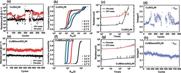
Figure 9. Comparison of characteristic curves between Cu/SiO2/W and Cu/MXene/SiO2/W devices: (a) and (e) ON and OFF resistance states extracted at 0.1 V; (b) and (f) multiple resistance states of the devices extracted at different voltage; (c) and (g) retention measurements for the devices under current compliance limit of 10 uA, read at 0.1 V; (d) and (h) operating voltage per cycle of both devices. Reprinted from [122], with the permission of AIP Publishing.
Download figure:
Standard image High-resolution imageThe cycling performances of the Cu/MXene/SiO2/W and Cu/SiO2/W devices were examined at the current compliance limit of 10 μA for up to 800 cycles and 600 cycles, respectively. The ON and OFF resistance states of the two devices extracted at 0.1 V are depicted in figures 9(a) and (e). The cumulative distributions of different resistance states for the two devices before the RESET and SET transitions are shown in figures 9(b) and (f). Obviously, the Cu/MXene/SiO2/W device exhibited more stable ON and OFF resistance states compared to the Cu/SiO2/W device. The resistance states of the Cu/SiO2/W device are relatively unstable and overlapping with each other. In comparison, the Cu/MXene/SiO2/W device displayed more consistent performance with distinguished multilevel RS states before both the RESET and SET transitions. Additionally, a relatively high retention of both ON/OFF states for Cu/MXene/SiO2/W devices can be observed in figures 9(c) and (g). Regarding the stability of the two devices, the distribution of the SET voltages (figures 9(d) and (h)) is stable and concentrated for the Cu/MXene/SiO2/W device, with most values of the SET voltage being around 0.78 V. Therefore, the Cu/MXene/SiO2/W memristor holds potentials for multilevel-cell memory and neuromorphic computing applications.
4.2. MXene/TiO2-based memristors
In 2020, a nano-floating-gate transistor memory (NFGTM) device was developed using MXene-TiO2 core-shell nanosheets, prepared through an aqueous processing method combined with oxidation [124]. The multilayer MXene and TiO2 acted as the floating gate and tunneling layer, respectively. The schematic illustration of the device is shown in figure 10(a). The memory performance of the NFGTM devices could be readily controlled by the oxidized TiO2 layer. When MXene is not presented in the device, its memory capacity can be disregarded. Upon introducing Ti3C2X, the device's memory window expands to 4.2 V. Subsequently, by forming a TiO2 layer on the MXene's surface, the memory window of the device significantly increases to 20.6 V (figures 10(b) and (c)). Expanding the scanning range to ±50 V allows the device's memory window to reach up to 35.2 V (figures 10(d)–(f)). Furthermore, the device demonstrates an ultra-low turning off current (<1 pA) and a high programming/erasing current ratio (≈106) (figure 10(g)). The device exhibits excellent cyclic stability over 1000 programming/erasing cycles (figure 10(h)). Furthermore, the device could be used to realize various synaptic functions, such as EPSCs, inhibitory postsynaptic currents (PSCs), PPFs, and long-term potentiation/depression synaptic plasticities. These functionalities demonstrate the potential of the device as a memory component for data storage applications.
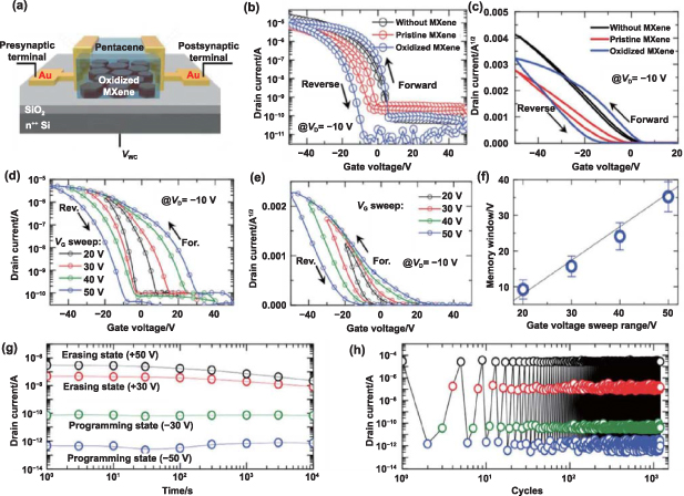
Figure 10. Structure schematic of the MXene-TiO2 memory device and its performance curves: (a) Structure diagram, (b) semi-log and (c) linear plots of transfer curves of the memory devices with various hysteresis behaviors, (d)–(f) transfer characteristics of the memory devices in different VG sweep ranges, (g) Retention and nonvolatile properties of the devices, (h) stability of the device over 1000 programming/erasing cycles. [124] John Wiley & Sons.© 2020 WILEY‐VCH Verlag GmbH & Co. KGaA, Weinheim.
Download figure:
Standard image High-resolution imageIn 2021, an optoelectronic memristor was fabricated with silver nanoparticles (Ag NPs) and Ti3C2/TiO2 hybrid nanosheets through a hydrothermal oxidation process [125]. By controlling the ultraviolet (UV) radiation intensity and pulse voltage, multiple resistance states (RS) could be achieved in the memristor devices with high repeatability and stability. Furthermore, a 4-bit binary comparator was constructed by utilizing the different RS behaviors of the memristor. A single comparator device could be used to partially realize logic gate function using the UV-controllable resistance state. The devices were characterized by operating input factors of VSet, VReset and UV light radiation, and corresponding output factors of HRS, LRS and MRS. The switching behaviors between the three pairs of resistive states could be controlled by regulating the pulse voltage and UV light radiation. The HRS of the device could be switched to LRS or MRS by applying SET pulse or UV light radiation. The MRS could be switched to HRS or LRS with the RESET pulse or the SET pulse. The MRS-LRS transition could be achieved with a SET pulse, while LRS to MRS transition was not available due to the nature of the nanosheet materials. These MXene hybrid comparators required fewer devices and could be easily scaled for practical applications compared to traditional digital comparators. In the same year, V2C MXene was used to develop Ag/V2C/TiO2/W memristor devices [126], exhibiting the coexistence of volatile TS and non-volatile memory switching (MS) behaviors, with low SET and RESET voltages as well as cycling and device stability.
4.3. MXene/ZnO-based memristors
In 2021, a Ti3C2–ZnO memristor was reported for possible multi-modal in-sensor computing [127]. The multiple-modal Ti3C2–ZnO memristors exhibited diverse functions, such as visual data sensing, relative humidity (RH) sensing, and preprocessing capabilities, emulating the environmental adaptive behaviors of human eye. The photon-/protons-controlled generation of oxygen vacancy filaments was responsible for the multiple-field resistance switching behavior of the Ti3C2–ZnO memristor device. In-sensor computing was realized by the Ti3C2–ZnO memristor, demonstrating the functions of a filter for information preprocessing and a synapse for implementing a weight-updating process with RH adaptability. Such a multimodal in-sensor computing device could reduce the underlying circuitry complexity of traditional neuromorphic visual systems, making it possible to develop device-level intelligence.
4.4. MXene/PZT-based memristors
Besides the traditional memristor devices, ferroelectrics have been acknowledged as potential candidates for memristor applications [128], offering simple structure, multiple resistance states, fast switching rate, and low power consumption level [129–132]. However, ferroelectric memristor devices encounter issues such as low durability, variable working voltage, and low switching ratio, which prevent them from achieving effects similar to those of biological synapses. In this regard, MXenes have been employed to modify the electrical performances of ferroelectric phases in order to improve the properties of ferroelectric memristor devices. A Cu/MXene/PZT/Pt hybrid ferroelectric memristor was explored using PZT with the composition of PbZr0.52Ti0.48O3 [133].
The ferroelectric-MXene memristor exhibited enhanced performance, including lowered switching voltage, reduced power consumption (figure 11(a)), improved stability, and enlarged switching ratio, compared to the Cu/PZT/Pt device (figure 11(b)). Benefiting from the suppression of the interface barrier, the formation of conductive filaments, and the vital role of MXene in the state switching processes, the Cu/Ti3C2/PZT/Pt ferroelectric memristors demonstrated impressively excellent performances (figure 11(c)). Moreover, the Cu/MXene/PZT hybrid ferroelectric memristor was employed to emulate biological synapses, exhibiting functionalities such as LTP and LTD (figure 11(d)), PPF, and STDP (figures 11(e) and (f)). The neural network structure of the memristor-based multilayer perceptron (MLP) is schematically depicted in figure 11(g). The input-hidden and hidden-output layers were connected through the synaptic weights of the Cu/MXene/PZT/Pt memristors. The edges of the MNIST handwriting images were cropped with 20 × 20 pixels. The networks were pre-trained using forward and backward propagations with 6 × 10⁴ random images in the database before the training of the networks. Images of 8 × 10³ per epoch were used for the training. Leaning accuracy was obtained by determining the percentage of correctly recognized numbers from 0 to 9. The recognition accuracy versus the number of epochs is shown in figure 11(e). The synaptic behaviors of the memristor devices enabled handwritten pattern recognition with an accuracy of 95%.
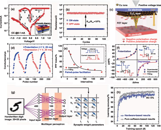
Figure 11. Characteristic curves of MXene-PZT memristors and neural network structure and performance based on memristors: (a) current-voltage characteristic of MXene-PZT memristors (inset diagram). Process 1–3 is the SET process and process 4–7 is the RESET process. (b) Endurance (cycle-to-cycle) of HRS and LRS for 100 cycles. The switching ratio is 104. (c) The process of forming Cu conductive path when the MXene-PZT memristive device was applied with positive voltage bias. (d) The gradual regulation of conductance states by continuous positive pulses (+1 V, 20 ms) and negative pulses (−1 V, 20 ms). The simulation of typical (e) PPF and (f) STDP behaviors of the devices, the insets display the pulse protocol. (g) The schematic diagram of memristor-based MLP neural networks: input layer, one hidden layer, and output layer, and weights are presented by the conductance of the Cu/Ti3C2/PZT/Pt memristive devices. (h) The relationship between recognition accuracy and training epochs. Reprinted from [133], © 2022 Elsevier Ltd and Techna Group S.r.l. All rights reserved.
Download figure:
Standard image High-resolution image4.5. MXene/SnS-based memristors
Besides oxides, other compounds (e.g. sulfides) have also been incorporated with MXenes to construct memristor devices. For instance, a SnS/MXene mixed hybrid was taken to fabricate asymmetric memristors with the advantages of cost-effectiveness, high energy-efficiency, and simple processing [134]. The SnS/MXene memristors were assembled by sandwiching the SnS/Ti3C2Tx active layer with Cu electrodes. An OFF/ON resistance ratio of 22 was achieved, along with a high cycling stability, reproducibility, and data retention capability of 1000 cycles. The memristor behaviors could be interpreted with a dual ionic conduction mechanism, where trapping and de-trapping of the charge carriers were responsible for the asymmetric behaviors of the memristors.
4.6. MXene/GST-based memristors
Chalcogenides, especially Ge2Sb2Te5 (GST), have been extensively studied for the applications of phase-change RAMs (PCRAMs) due to their reversible switching behavior between crystalline and amorphous states when stimulated with electrical current or laser pulse [135–138]. However, GST PCRAMs encounter shortcomings such as high programming current accompanied by high power consumption, and the phase transition rate is still not sufficiently high for practical applications [139, 140]. Therefore, it is natural to consider constructing memristors by combining GST with MXene. In 2023, a low-power artificial neuron with an Ag/MXene/GST/Pt memristor was demonstrated to exhibit promising TS performances [141]. Specifically, the devices had a low SET voltage of 0.38 V, a current of 200 nA, a slope of <0.1 mV dec−1, and a large OFF/ON ratio of > 103. Furthermore, the characteristics of integrate and fire neurons that are indispensable for spiking neural networks were experimentally demonstrated. Finally, the memristive mechanism was interpreted through the first-principle calculation based on the electrochemical metallization effect.
Cycling performances of the Ag/MXene/GST/Pt devices were experimentally compared to those without the presence of GST [141]. Representative I–V curves of the Ag/GST/Pt and Ag/MXene/GST/Pt devices at currents of 10 mA and 5 μA are shown in figures 12(a) and (b), respectively. Obviously, the Ag/GST/Pt device displayed strong cycling endurance and stable bi-directional TS effect, while the SET voltage and current were quite high, with values of 1.6 V and 1.4 mA, respectively. In comparison, the Ag/MXene/GST/Pt device had a SET voltage of 0.38 V and a current of 200 nA, significantly reducing power consumption. In addition, the SET voltage in positive polarity exhibited a relatively narrow distribution compared to negative polarity. Ag+ ions were trapped in the GST layer after the sweep of positive voltage, migrating back to the Ag top electrode. Therefore, a conductive bridge was formed due to the sweep of negative voltage. Once the Ag+ ions were absent, the conductive bridges became more random in the GST layer, resulting in a wide distribution of the SET voltage. Notably, the Ag/MXene/GST/Pt device in positive polarity had SET voltages ranging from 0.2 V to 0.4 V, and the SET power consumption was calculated to be in the range of 10–100 nW. Figure 12(c) shows cycling stability of the Ag/MXene/GST/Pt device after 300 cycles of DC voltage sweeps. The Ag/MXene/GST/Pt device was also evaluated by different pulse amplitudes, with the experimental results depicted in figures 12(d)–(f). With increasing pulse amplitude, the stability of the resistance states was increased, whereas the OFF/ON resistance ratio was larger than 103. When the pulse amplitude was too low, the electric field was insufficiently strong to ensure the formation of conductive bridges by the Ag+ ions. In other words, the device performance could be maintained by adopting appropriate pulse amplitude and pulse width.
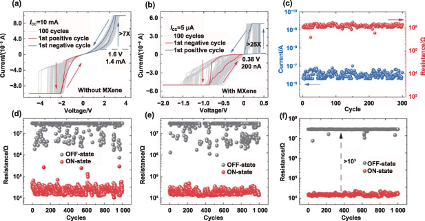
Figure 12. Characteristics curves and endurance performance of the memristors: threshold switching (TS) I–V characteristics of the (a) Ag/GST/Pt and the (b) Ag/MXene/GST/Pt memristors. (c) Endurance testing results of the Ag/MXene/GST/Pt device for DC voltage sweeps up to 300 cycles. ON and OFF resistance states by using current pulses at different amplitudes for write and 10 nA amplitude for read: (d) 5 uA, (e) 10 uA and (f) 50 uA. Pulse width and interval were both 20 ms. Reproduced from [141]. © 2023 Chinese Physical Society and IOP Publishing Ltd. All rights reserved.
Download figure:
Standard image High-resolution image4.7. MXene/lithium polymer electrolytes (LPE)-based memristors
Synaptic devices can be realized by utilizing the transportation behaviors of cations. Due to the small size and light weight, Li+ ion has various advantages for applications in synaptic devices, such as low energy consumption, multiple storage state, and stable performance. The incorporation of MXene and LPE has been an interesting topic in the development of synaptic devices. For instance, Au/LPE/Ti3C2/Si memristor was fabricated to display artificial synapse [142], in which the adsorption-desorption or insertion-extraction of Li+ ions was used to simulate various functions, including latent plasticities, memory enhancements, dendritic integrations, and Pavlovian learning capacities. The devices were advantageous in realizing the functions of dendritic integration and memory enhancement, owing to their relatively low power consumption and high sensitivity.
5. Application in neuromorphic devices
5.1. Data storage
MXene-based memristors have great potential applications in neuromorphpic systems, such as data and multi-level data storage, neural morphology computing, sensor computing, artificial synapse, and logic circuit. The functional layers can consist of single compositional MAXs, MXenes, or composites (hybrids) modified with other components. There can be single, double, and hetero-structures, as shown in the typical examples in table 3. One of the main applications of memristors is data storage. This function is realized through the switching phenomenon resistance of the memristors. When memristor has multi-level storage capacities, they can meet the urgent needs of new types of storage, such as high-density data storage. MXenes-based memristors have great development potential for real applications because of their high switching speed, simple device fabrication process, low power consumption, and CMOS compatibility. Typically, a memristor consists of two electrodes and an MXene functional layer. When subject to external electric fields, the memristors display switching between HRS and LRS. In digital circuits, HRS corresponds to the low potential level ('0'), while LRS corresponds to the high level ('1'). As a result, the switch from HRS to LRS is similar to the binary conversion from '0' to '1' in the data storage processes.
Table 3. Different applications of memristive devices based on MXenes.
| Application | Structure | Functional layer | References |
|---|---|---|---|
| Data storage | Pt/Ti3C2Tx /Pt | One-component | [119] |
| Pd/MoOX/Mo2C/Au | Laminated construction | [143] | |
| Cu/Ti3C2/SiO2/W | Laminated construction | [112] | |
| Au/Ti3C2Tx @PVP/rGO | Composites | [144] | |
| Au/Ti3C2Tx QDs@PVP/ITO | Composites | [145] | |
| Au/(AgNPs)Ti3C2-TiO2/ITO | Composites | [125] | |
| Multilevel data storage | Al/Ti3C2Tx -OP/ITO | Composites | [99] |
| Al/Ti3C2Tx @PVPy/ITO | Composites | [146] | |
| Neuromorphic computing | Ag/V2C/W | One-component | [107, 118] |
| Cu/Ti3C2/Cu | One-component | [103] | |
| TiN/Cu/Ti3C2/SiO2/TiN | Laminated construction | [123] | |
| Al/Ti3C2@Ag/Pt | Composites | [32] | |
| In-sensor computing | ITO/Ti3C2-ZnO/Al | Composites | [127] |
| Artificial synapse | Ag/Ti3C2Tx /Pt | One-component | [119] |
| Al/Ti3C2Tx /Pt | One-component | [119] | |
| Ag/V2C/TiO2/W | Laminated construction | [126] | |
| Ag/Ti3C2/SiO2/Pt | Laminated construction | [116] | |
| Cu/Ti3C2/SiO2/W | Laminated construction | [112] | |
| TiN/Cu/Ti3C2/SiO2/TiN | Laminated construction | [123] | |
| Logic circuit | Au/(AgNPs)Ti3C2-TiO2/ITO | Composites | [125] |
In 2019, Zhang et al reported Ti3C2 MXene-based two-terminal memristive devices with a configuration of Cu/Ti3C2/SiO2/W (figure 13(a)) [147]. The devices exhibited bipolar RS behavior (figure 13(b)) when scanning voltages were applied between −2.5 and +2 V. With the presence of the MXene functional layer, the device had a retention time of 103s (figure 13(c)). In the same year, Ding et al used Ti3C2-PVPy hybrid to develop memristors [146]. In this case, forming-free bipolar RS behavior was observed when non-volatile resistive random access memories (RRAMs) were considered. Since the VSET was as low as 0.5 V, it could be used to develop low-energy consumption devices. Typical I–V curves of the RRAM devices are shown in figure 13(d), while resistance switching behaviors based on charge trapping and conductive paths (CPs) are depicted in figure 13(e). It is worth mentioning that different current levels were well maintained for ten continuous cycles of voltage pulses at different values of ICC in the SET process (figure 13(f)). This observation suggests that Ti3C2 MXene-based RRAMs could be utilized for multilevel data storage. As seen in figure 13(g), 'FMEG' characters could be stored in a certain unit of the storage array by setting different values of ICC. Afterward, the LRS current value at −0.3 V could be read to obtain the stored information (figure 13(h)). In 2020, Mao et al employed Ti3C2Tx MXene quantum dots (QDs) as the function layer to realize memristor effect with a structure of ITO/MQDs-PVP/Au [145]. The devices exhibited strong bipolar RS behaviour. After 50 consecutive cycles, high conductivity could be well maintained, together with excellent accuracy (figure 13(i)), a high current ratio of up to 102 (figure 13(j)), strong retention exceeding 1.2 × 10⁴ s, and a very narrow SET/RESET voltage distribution (figure 13(k)). Such adjustable memory and transient characteristics ensure safe data storage.

Figure 13. MXenes based memristors and their applications in data storage: (a) schematic structure, (b) I–V characteristics and (c) retention stability of Cu/Ti3C2/SiO2/W memristive device. Reprinted from [147], © 2019 Elsevier Ltd and Techna Group S.r.l. All rights reserved. (d) I–V curve and (e) the resistive switching mechanism based on charge trapping and conductive paths (CPs) of Al/Ti3C2@PVPy/ITO memristor device. (f) Reversible RS over 60 cycles with various current compliances of Ti3C2-based RRAM, (g) basic operating principle of the RRAM array using different ICC , (h) LRS current values of the cells under different ICC in SET process (1 V) in the 13 × 13 RRAM array (read: −0.3 V). Reproduced from [146] with permission from the Royal Society of Chemistry. (i) The I–V cycle, (j) retention characteristics, and (k) SET voltage probability distributions for the setting processes of ITO/MQDs-PVP/Au memory device. [145] John Wiley & Sons. © 2019 WILEY‐VCH Verlag GmbH & Co. KGaA, Weinheim.
Download figure:
Standard image High-resolution image5.2. Artificial synapses
The typical structure of MXene-based memristors generally consists of two electrodes (top and bottom) with the MXene functional layer in between, thus being similar to two neurons in contact with each other (figure 14(a)). Therefore, the resistance of memristor can be readily varied by adjusting the migration rate of ions, simulating the transmission behaviors of ions in biological synapses and enabling the construction of artificial synapses [148]. For example, Zhao et al reported an artificial synaptic device with ZTO/MXene/SiO2 as the functional layer, as shown in figure 14(b) [149]. They used the device to simulate bioelectric signals of presynaptic voltage (Vpre) by applying electrical spikes to the bottom electrode, while measuring the triggered drain-source current to simulate the bioelectric signal of PSC. EPSC characteristics with ten pulses of variable height and width are illustrated in figures 14(c) and (d). Figure 14(e) shows the simulation results of the synaptic devices on memory. If pulse induction is considered as a learning process (red part in the figure), the retention time of EPSC after the disappearance of Vpre represents a forgetting process (blue area). This phenomenon is similar to the prolongation of the forgetting period of memory after reinforcement learning, which is in agreement with the Ebbinghaus Forgetting law. Further experimental results demonstrate that the device has excellent stability against pulse cycling stimuli (figure 14(f)). Yan et al developed a new memristor for simulating the synaptic plasticity based on Ti3C2Tx MXene [121]. The device exhibited repeatable RS behaviors (figures 14(g) and (h)) and an extremely fast response rate to pulse stimuli (figures 14(i)–(l)). More importantly, the transition from STP to LTP was achieved at the nanosecond scale for the first time.

Figure 14. MXenes-based memristors and their applications in artificial synapses: (a) Schematic diagram of synaptic signal transmission in biological system. (b) The structure diagram of the artificial synapse device based on MXenes. The EPSC behavior of the device's response to various heights (c) and widths (d) of gate pulse. (e) The memory behavior of device changing from STM to LTM with an increasing number of pulses. (f) Cyclic stability of devices on 550 negative-positive pulse pairs. [149] John Wiley & Sons. © 2021 Wiley‐VCH GmbH. (g) The potentiation and (h) depression curves of the memristor device based on Al/Ti3C2Tx /Pt when subject to successive alternating current pulses. Initial data of continuous pulse regulation with different pulse durations (i), (j) and amplitudes (k), (l). [121] John Wiley & Sons. © 2019 WILEY‐VCH Verlag GmbH & Co. KGaA, Weinheim.
Download figure:
Standard image High-resolution image5.3. Neural morphological computations
The application of MXene-based memristors in the field of neural morphological computation is an important direction. Wang et al reported Ti3C2–ZnO-based multimodal flexible sensing memristors that combined visual data detection, humidity detection, and preprocessing functions, successfully simulating the environmental adaptability of neuromorphic visual systems [127]. For in-sensor computing applications, the device was built with 28 × 28 input neurons and 10 output neurons, with fully connected 785 × 10 synaptic weights (figure 15(a)). The synaptic weight was adjusted through humidity and light modulation. The device displayed long-term potential characteristics when subject to 50 light pulses, while long-term depression characteristics were observed when 50 electrical pulses were applied (figure 15(b)). Objective output images of the device, with '1–9' digital combinations after training at different RH levels, are illustrated in figure 15(c). After training at 60% RH, the artificial vision network was able to capture more features from the selected letters. With 6 × 10⁴ training epochs, high recognition accuracy could be achieved at different RH levels (figure 15(d)). Therefore, with multimodal in-sensor computing, the underlying circuit complexity of traditional neuromorphological vision systems could potentially be reduced, while power consumption and chip area could be significantly decreased. This indicates the MXene-based memristors have strong potentials for the development of intelligence in device-level implementations.

Figure 15. Real-time training for image recognition of Ti3C2–ZnO memristors. (a) Schematic illustration of the high-level in-sensor computing by employing the sensing memristor as a synapse to implement weight updating. (b) RH-mediated plasticity of the device showing long-term enhancement and long-term suppression when subject to optical and electrical pulses. (c) Output image after 6 × 10⁴ training epochs for the sensing memristor at different RH levels. (d) Recognition rate as a function of RH level. [127] John Wiley & Sons. © 2021 Wiley‐VCH GmbH.
Download figure:
Standard image High-resolution image
5.4. Logic circuits
In addition to their applications in data storage, neuromorphic computing, and artificial synapse, MXenes-based intelligent devices are also promising for applications in logical operations. These devices might overcome the shortcomings of the traditional integrated logic circuits, such as voltage loss and high energy consumption, offering new solutions for low-power logic operations. For instance, Guo et al developed cost-effective optoelectronic RRAMs based on Ag nanoparticles-MXene-TiO2 nanosheets [125]. They realized the function of replacing five logic gates in traditional chips with a 4-bit in-memory digital comparator, simplifying complex logic operations. With the development of new materials and the discovery of special properties of MXenes, their applications in the fields of neural morphology devices and AI are expected to become increasingly popular.
6. Summary and outlooks
MXenes have emerged as a new group of 2D materials with multiple functions for neuromorphic device applications. The conductive filaments are the main working mechanism of memristor devices related to the active materials and electrodes. Compared to the traditional metal oxide memristive devices, MXene-based devices are advantageous for smaller dimension, lower power consumption, and higher flexibility. Moreover, with unique structures, MXene nanosheets provide a powerful platform for the incorporation of other functional materials to construct memristors with desirable performances. Although significant progress has been made in MXene-based neuromorphic applications, further efforts are needed.
- (I)The synthesis of single- or fewer-layer MXenes with large-scale production and high quality is still a challenge that requires further exploration. Most of the reported MXene-based neuromorphic devices are based on Ti3C2Tx materials, and more MXene materials should be synthesized and developed for effective and potential memristors for practical applications.
- (II)MXenes have abundant surface-active functional groups that may be sensitive to air (O2) and water (H2O) molecules. The long-term environmental stability of MXene-based memristors should be improved for practical application. On the other hand, appropriate surface engineering related to the surface-terminated functional groups can greatly modify the performance of memristor devices.
- (III)With their unique 2D structures and abundance of terminated functional groups, MXene nanosheets offer a powerful platform for incorporating more functional materials to construct memristors with desirable performance.
- (IV)The development of highly integrated 3D synaptic electronic devices with multiple input and output signal conversions will become a core area of future exploration to achieve the complete synaptic function of artificial neural networks.
- (V)Optical signals have been incorporated into memristor devices. Another important research direction is the combination of MXene with other light-sensitive nanomaterials to construct higher-performance optically stimulated synaptic memristor devices, introducing an additional regulated dimension of photoelectron.
- (VI)Most studies are still focused on utilizing devices with different structures and materials to generate memristor behaviors for the simulation of biological synapses. How to use memristors to realize the function of neuromorphological systems deserves further study as a long-term topic in the future.
Acknowledgments
This work was supported by National Natural Science Foundation of China (52172205, 52172070 and 51962013), Jiangxi Provincial Science and Technology Projects (20232ACB204009, 20223AAE02010, 20201BBE51011, jxsq2019201036 and GJJ201319), Innovation Enterprise Program of Shandong Provincial (2023TSGC0469), Guangdong Basic and Applied Basic Research Foundation (2020B1515120002), General Projects of Shenzhen Stable Development (SZWD2021003), and University Engineering Research Center of Crystal Growth and Applications of Guangdong Province (2020GCZX005).