
Highlights
The significance and universality of meniscus-on-demand 3D printing method for micro- and nano-fabrication are introduced.
The theoretical dynamics and physics behind the meniscus formation are summarized.
The applicability to various printable materials and capabilities for fabrication of photonic and electronic devices are demonstrated.
The existing challenge and potential research opportunities in terms of micro/nano-scale meniscus-on-demand 3D printing are pointed out.
Abstract
The continual demand for modern optoelectronics with a high integration degree and customized functions has increased requirements for nanofabrication methods with high resolution, freeform, and mask-free. Meniscus-on-demand three-dimensional (3D) printing is a high-resolution additive manufacturing technique that exploits the ink meniscus formed on a printer nozzle and is suitable for the fabrication of micro/nanoscale 3D architectures. This method can be used for solution-processed 3D patterning of materials at a resolution of up to 100 nm, which provides an excellent platform for fundamental scientific studies and various practical applications. This review presents recent advances in meniscus-on-demand 3D printing, together with historical perspectives and theoretical background on meniscus formation and stability. Moreover, this review highlights the capabilities of meniscus-on-demand 3D printing in terms of printable materials and potential areas of application, such as electronics and photonics.
Export citation and abstract BibTeX RIS

Original content from this work may be used under the terms of the Creative Commons Attribution 4.0 license. Any further distribution of this work must maintain attribution to the author(s) and the title of the work, journal citation and DOI.
1. Introduction
Three-dimensional (3D) printing is a form of additive manufacturing and one of the most disruptive technologies to emerge in recent years. It has attracted increasing attention owing to its possible applications in the manufacturing industry, which could lead to benefits for economies and people's daily lives [1]. In particular, 3D printing could be used to unify the traditional manufacturing processes of molding, carving, welding, and assembly, and thereby underpin simple, versatile, and sustainable manufacturing routes [2]. The potential economic impact of 3D printing on manufacturing industry is huge [3], with an expected growth of US$200 billion per year by 2025 [4]. However, the utilization of conventional 3D printing methods, such as stereolithography and fused deposition modeling, has long been restricted to prototyping rather than direct manufacturing, owing to the technological challenges associated with material and precision [5–9]. Over the past two decades, substantial research progress has been made in meeting these challenges. First, the invention of two-photon lithography has resulted in a breakthrough in the precision of 3D printing. This technique exploits the nonlinear dependency of polymerization rate on the intensity of irradiating light to produce 3D structures with feature sizes beyond the diffraction limit [10–12], which is a key step toward nanoscale 3D printing. Second, the utilization of viscoelastic colloidal inks for nozzle-based extrusion 3D printing has contributed to the diversification of 3D printable materials to include polymers, metals, and ceramics [13, 14]. Nevertheless, it remains a technological challenge to obtain both nanoscale-precision and material diversity.
A liquid meniscus formed between a sharp tip and a substrate can drive effective material transport/assembly at the nanoscale. Dip-pen nanolithography involves the use of a nanosized ink meniscus [15] formed on an atomic-force microscope tip to draw two-dimensional (2D) nanopatterns on a planar substrate under the effect of solvent evaporation [16]. Moreover, recent studies have demonstrated that a fluid-like ink meniscus formed on a nanopipette can be used for 3D printing, during which the nanopipette continuously supplies ink. This process is referred to as meniscus-guided 3D printing. Crucially, the mechanical flexibility of the meniscus allows the spatial resolution to be controlled at ∼100 nm without nozzle clogging, which has been a longstanding problem that has limited the application of nozzle-based 3D printing. Subsequent rapid solidification via solvent evaporation enables the retention of printed 3D nanostructures. This meniscus-guided method is also compatible with diverse materials, including polymers [17], metals [18], carbon nanomaterials [19], perovskites [20], and metal–organic frameworks (MOFs) [21]. These technological advancements in terms of precision and materials offer new avenues for the direct manufacture of electronics and photonics via 3D printing.
This review presents recent advances in research on meniscus-guided 3D printing technologies for manufacturing freeform electronic and photonic devices. First, we briefly discuss the formation and utilization of a femtoliter ink meniscus for micro/nanoscale 3D printing. Then, we describe the various materials printable via the meniscus-guided method, including metals, polymers, carbon nanomaterials, MOFs, peptides, and perovskites, and their applications in electronic and photonic devices. Finally, we outline the challenges and prospects for the development of meniscus-guided 3D printing technology for use in integrated circuit manufacturing.
2. Theoretical background
2.1. Meniscus formation
The meniscus-guided 3D printing process employs a femtoliter-volume Newtonian ink meniscus to write freeform 3D micro/nanostructures under rapid evaporation of solvent. The first step is the production of an ink meniscus between a nanopipette tip and a substrate. The success of the printing process relies on understanding the dynamics of meniscus formation. As such, three methods have been devised for the formation of an ink meniscus: physical contact, electrohydrodynamic (EHD) dispensing, and pressure-induced dispensing.
Figure 1(a) depicts the physical contact method of meniscus formation. First, an ink-filled nanopipette touches a substrate surface, resulting in a femtoliter-volume of ink being dispensed via wetting to form a meniscus at the nanopipette–substrate gap. Then, the solvent rapidly evaporates on the meniscus surface, accelerating the solidification. Subsequent upward movement of the nanopipette results in meniscus formation and solidification on the previous solidified structure front. Thus, when the meniscus is stable between the nanopipette tip and the top of the as-printed structure during nanopipette movement, continuous nanoscale printing is realized [17, 22–25]. This physical contact method is a minimalist way of producing an ink meniscus, as it requires no external fields or additional steps. However, the reliability of this method is limited, owing to inconsistent nanopipette–substrate contact behavior and nanopipette tip breakage due to repeated contact. Solving these problems is crucial for establishing a high-throughput, scalable printing process.
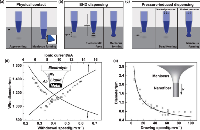
Figure 1. Meniscus-formation and thermodynamic stability. Schematic showing three meniscus-formation mechanisms: (a) physical contact; (b) electrohydrodynamic (EHD) dispensing; and (c) pressure-induced dispensing. (d) Meniscus Thermodynamic stability window of an electrolyte meniscus for stable 3D electrodeposition. From [30]. Reprinted with permission from AAAS. (e) Plot of nanowire diameter versus drawing speed during the meniscus guided process. [22] John Wiley & Sons.
Download figure:
Standard image High-resolution imageThe development of non-contact procedures can considerably improve the reliability of meniscus formation. For example, Chen et al reported an EHD method for forming a femtoliter ink meniscus; crucially, this method does not involve nanopipette–substrate contact and positional feedback, and is applicable to nanoscale, parallel 3D printing [26]. As illustrated in figure 1(b), the method begins with placement of an ink-filled nanopipette a few micrometers away from a substrate. Subsequently, a voltage with a programmed pulse is applied to the substrate to generate electric charges on its surface, which results in the formation of an electrostatic attractive force between the charged substrate and the ink surface at the nanopipette tip. The electrostatic force ultimately overcomes the surface tension of the ink, resulting in dispensing of the ink and the formation of a femtoliter ink meniscus at the nanopipette–substrate gap. The meniscus can be used to draw freeform 3D nanostructures under the effect of solvent evaporation. The reliability of this non-contact, feedback-free, electrostatic method enables its use in nanoscale parallel manufacturing.
Additionally, an ink meniscus can be easily produced if a pendant ink droplet is formed at a nanopipette tip under pneumatic pressure, particularly when highly viscous inks such as polymer or liquid metal inks are used [27–29]. This is because a pendant ink droplet enables the formation of an ink meniscus with only moderate-pressure contact (rather than extensive physical contact) between a nanopipette and a substrate, which also helps to maintain stable meniscus formation during the printing process. Moreover, the application of backpressure instantly terminates the printing process. This pressure-assisted approach produces a larger meniscus volume than the other two methods do, widening the printing width.
2.2. Meniscus stability
The mechanical flexibility of a meniscus allows for printing structures finer than a nanopipette aperture by the application of stretching. One study achieved ∼100 nm spatial resolution using a femtoliter ink meniscus formed on a 1–2 µm-diameter nanopipette by increasing the nanopipette withdrawal (pulling) speed [20]. Such resolution has not been obtained via other nozzle-based 3D printing techniques. It is critical to maintain the thermodynamic stability of the meniscus formed between a nanopipette and the growth front of a printed structure during continuous nanopipette withdrawal. The thermodynamic stability is determined by the thermodynamic properties of the ink and the involved interfaces. As depicted in figure 1(d), with the thermodynamic consideration, the interfacial forces at the three-phase contact line between the meniscus and the growth front should satisfy the Neumann quadrilateral relation with an equilibrium angle, ϕ0, between the growth direction and the meniscus surface as follows [30]:
where  and
and  are the surface energies of the ink and the grown solid, and
  is the interfacial energy of the ink–solid interface. Within the stable meniscus region, the deviation of ϕ allows for control of the diameter of the grown structure through adjustment of the nanopipette withdrawal speed [31]. Furthermore, to continue the printing process, the radius (
 )–drawing speed (
 ; same as nanopipette withdrawal speed) relationship should satisfy the following material balance law:

where  is the mass rate of solute precipitation, and
  is the density of the grown solid structure. An inverse square root dependence of diameter on drawing speed was observed in a previous study (figure 1(e)) [22]. It is also critical that the solute precipitation rate can be influenced by the solvent evaporation [17, 20, 32]. A critical drawing speed exists; at speeds below this critical drawing speed, continuous, uniformed printing is realized, whereas at speeds above this critical drawing speed, a meniscus is unstable and prone to break off from a nanopipette, resulting in discontinuous growth.
3. Printing materials and applications
3.1. Metals
Metals are essential elements for integrating electronic and photonic circuits, owing to their outstanding electrical, optical, and mechanical properties [33–35]. For example, highly conductive metallic interconnects can serve as paths in a circuit to transmit signals and data among electronic devices [36–39]. In addition, nanoscale metallic materials, such as nanoparticles, can be used to manipulate electromagnetic fields at the subwavelength scale to produce nanophotonic device components [40, 41]. However, there is a need for a manufacturing method that enables the 3D integration of metallic components of chips, as this will increase their integration density and design flexibility. Recently, the meniscus-guided 3D printing method has been used to fabricate freeform metallic micro- and nanostructures with the aid of two material-growth pathways: (1) electrochemical deposition, and (2) nanoparticle assembly and annealing. First, we review recent advances in the meniscus-confined electrochemical deposition-based 3D printing of metallic structures and the electronic and photonic applications of these structures.
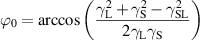
Figure 2(a) depicts the meniscus-confined electrodeposition process [42]. The printing apparatus comprises a glass nanopipette filled with an electrolyte, a metal wire (anode), and a conductive substrate (cathode) on which the metal is deposited. An electric potential is applied across the metal wire and the substrate, resulting in the electrodeposition process in an electrolyte ink meniscus formed between the nanopipette and the substrate. The deposition is guided vertically when the nanopipette is withdrawn from the substrate. Synchronization of the withdrawal speed of the nanopipette and the vertical growth of metal maintains the thermodynamic stability of the meniscus, resulting in continuous growth of a freestanding metallic structure [28, 43–45] (figure 2(b)).
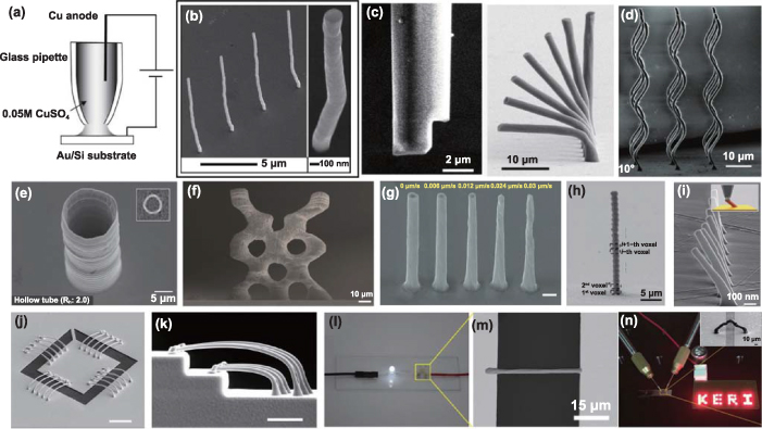
Figure 2. Electrodeposition-based meniscus-confined 3D printing of metallic nanostructures. (a) Schematic of setup for meniscus-confined electrodeposition 3D printing. (b) Scanning electron microscopy (SEM) images (tilted) showing an array of four Cu nanowires with diameters of 200–250 nm and a length of 10 µm, and an SEM isometric view of a Cu nanowire. Reprinted from [42], with the permission of AIP Publishing. (c) Electrodeposited Cu wires with different inclination angles fabricated using a side-cut micropipette. From [30]. Reprinted with permission from AAAS. (d) A Cu microhelix array. Reproduced from [46] with permission from the Royal Society of Chemistry. (e) Hollow tube structures. (f) Mesh structures. [23] John Wiley & Sons. (g) A Cu/Co microwire array with a diameter gradient. [47] John Wiley & Sons. (h) An SEM image of a vertical Cu microwire composed of 20 Cu voxels with a diameter of 1 µm. Reprinted from [48], Copyright 2022, with permission from Elsevier. (i) SEM images of tilted pillars with a lateral shift printed via voxel stacking, as illustrated in the inset. Reprinted with permission from [18]. Copyright 2021 American Chemical Society. (j) SEM images showing 20 electrodeposited interconnects with submicrometer diameters extending from a 50 µm × 50 µm central pad (scale bar: 10 µm). (k) SEM images showing overlap interconnects spanning 5 μm-high steps (scale bar: 10 μm). From [30]. Reprinted with permission from AAAS. (l)–(n) A lit LED lamp with single Cu structures as electrical interconnects. [23] John Wiley & Sons. Reprinted with permission from [50]. Copyright 2018 American Chemical Society.
Download figure:
Standard image High-resolution imageSome innovative strategies have been devised to achieve high resolution, omnidirectionality, and continuous printing. Hu et al devised a side-cut micropipette as a nozzle to facilitate both vertical and lateral printing. The geometry of the side-cut micropipette provides a stable and controllable meniscus during the omnidirectional printing process (figure 2(c)). In 2017, Yi et al demonstrated the 3D printing of intricate and high-degree-of-freedom metal microhelices with high electrical conductivity using a high-resolution monitoring system (figure 2(d)) [46]. Seol et al developed a voltage modulation-based method to control the formation of solid and hollow internal structures, respectively, during meniscus-confined 3D electrodeposition (figures 2(e) and (f)) [23]. Nie et al demonstrated the direct writing of shape-gradient magnetic alloy microwires through dynamic adjustment of pull-away speed in meniscus-confined electrodeposition (figure 2(g)) [47]. Other researchers have also developed voxelated meniscus-confined electrodeposition methods to produce freeform 3D metallic nanostructures [18, 48].
Metallic structures formed by the above-described methods have been utilized as interconnects in electronic circuits [40, 49]. Figures 2(j) and (k) show high-density, high-quality metallic interconnects extending from pads [29]. Figures 2(l)–(n) demonstrate the function of electrical interconnects directly printed onto light-emitting diode (LED) circuits [23, 50].
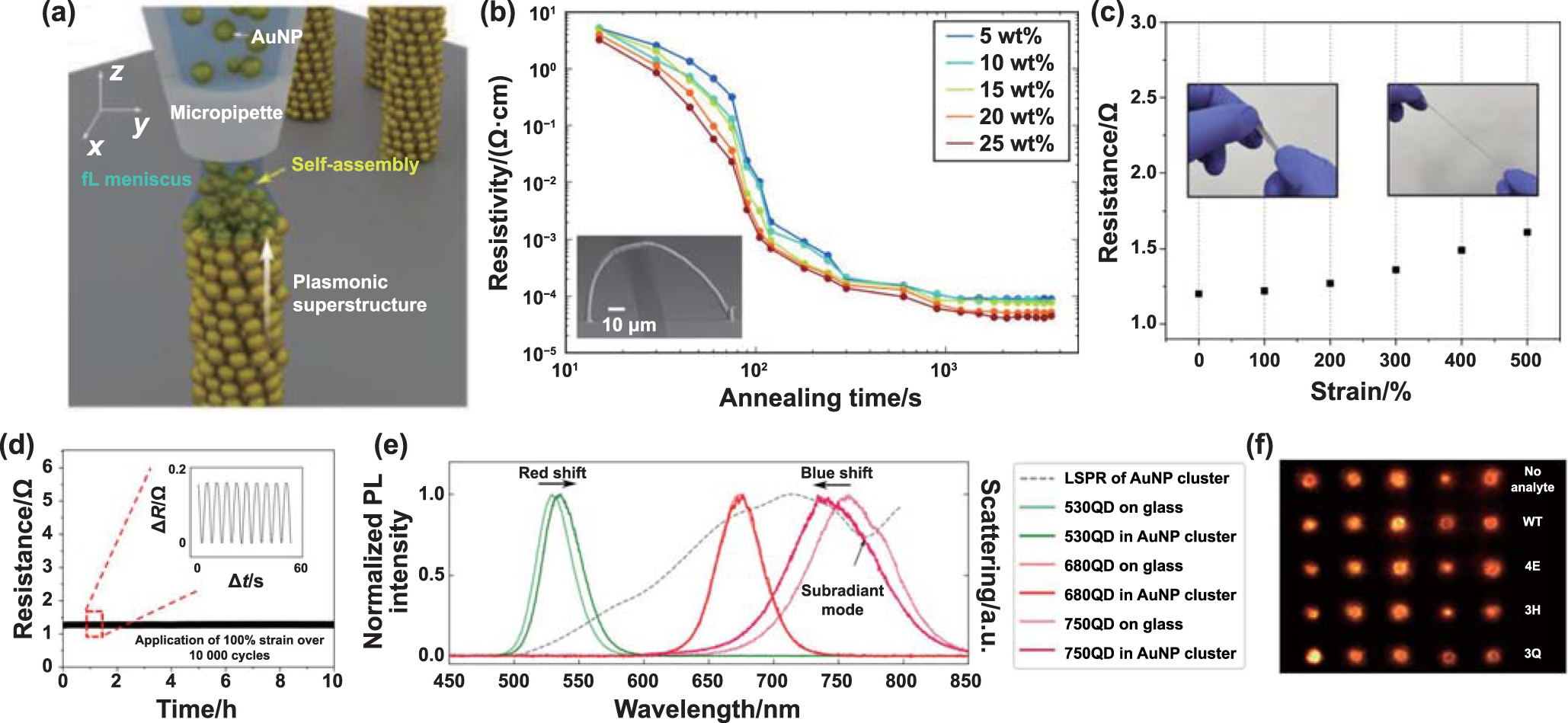
Meniscus-guided 3D printing can also be realized through the use of metallic nanoparticles-suspended solution as printing inks. Specifically, the liquid meniscus formed at a nanopipette–substrate gap can confine and guide the self-assembly of nanoparticles in three dimensions under the effect of solvent evaporation, thereby producing freestanding metallic microstructures (figure 3(a)). Subjecting a thus-printed metal structure to mild thermal or chemical annealing can endow it with sufficiently high electrical conductivity to be used for fabricating interconnects for flexible and wearable electronic circuitries. Lee et al used Newtonian polymer-capped silver nanoparticle inks for high-resolution 3D printing of microelectrodes with a diameter of ∼5 µm and an electrical conductivity of over 104 S cm−1, and subjected printed structures to post-thermal annealing (figure 3(b)) [51]. In 2022, Lee et al reported a one-step technique that employs a semi-solid polyelectrolyte-attached liquid-metal microgranular particle-based ink for printing highly conductive and stretchable microelectrodes [29], without the need for post-processing. The printed liquid-metal interconnect exhibited only a small change in electrical resistance under extreme stretching (500%; figure 3(c)) and no electrical failure under repeated strain (10 000 cycles; figure 3(d)). These properties will enable the practical application of such printed interconnects in soft electronics.
Figure 3. Meniscus-confined 3D printing of metallic nanoparticles. (a) Schematic of 3D printing of freestanding metallic nanostructures. Reprinted with permission from [53]. Copyright 2022 American Chemical Society. (b) Electrical resistivity of Ag electrodes (inset: field-emission scanning electron microscopy image) of various concentrations during thermal treatment. Reprinted with permission from [51]. Copyright 2017 American Chemical Society. (c) Resistance of printed PaLMP under strain. (d) Resistance of PaLMP under repeated application of 100% strain over 10 000 cycles. Reproduced from [29]. CC BY 4.0. (e) Photoluminescence (PL) spectral shifts of three quantum dots near-field-coupled to an AuNP cluster. (f) Dark-field scattering top-view images of pillar arrays containing various types of M13 bacteriophages. Reprinted with permission from [53]. Copyright 2022 American Chemical Society.
Download figure:
Standard image High-resolution imageThe meniscus-guided 3D printing method can also be used to create freeform plasmonic nanoparticle clusters with desired shapes and compositions. Kim et al demonstrated that the 3D geometry of printed quantum dot-embedded plasmonic clusters allowed for radiation pattern manipulation (figure 3(e)), and the plasmonic clusters exhibited enhanced sensitivity for virus detection (figure 3(f)) [52, 53]. Thus, such printed plasmonic structures could be used as high-sensitivity, cost-effective pathogen diagnosis platforms, which are in high demand for pandemic management.
3.2. Polymers
Polymer-based 3D printing inks are gaining increasing attention, owing to their excellent electrical and optical properties and ease of processing. Functional polymers have been utilized in various applications, such as soft electronics [54], biomedical engineering [55], energy storage [56], and smart sensors [57, 58]. Recently, several studies have reported the precise and rapid meniscus-guided printing of polymeric materials, including polypyrrole (PPy) [17, 24, 59], poly(3,4-ethylenedioxythiophene) polystyrene sulfonate (PEDOT:PSS) [60, 61], polyaniline (PANI) [62], polystyrene (PS) [63], chitosan hydrogel [64], and block copolymers [65]. The meniscus-guided method can pattern these polymers into micro/nanoscale structures with various morphologies, such as pillar arrays, arches, tubes, meshes, and walls, paving the way for new applications in electronics, mechanics, and photonics.
Polymer growth in the meniscus-guiding process occurs via (i) polymerization and (ii) evaporation-driven solidification. To polymerize a monomer ink meniscus during the guiding process, studies have employed oxygen in air as an oxidant [17] or applied an external electric potential [62]. The polymer solution meniscus can also be solidified via the rapid evaporation of solvent during the guiding process, to produce 3D micro- and nanostructures [60, 66, 67].
Meniscus-guided 3D printing technology allows for the rapid prototyping of stretchable conjugated polymer nanowires for electrode connection and light propagation. Kim et al demonstrated the 3D printing of high-aspect-ratio PEDOT:PSS nanoarch interconnects via evaporation-driven solidification (figure 4(a)) [60]. The connected working LED devices maintained their performance under extreme stretching conditions of up to 270% (figure 4(b)). Pyo et al reported similar stretchable connections for light propagation in straight, curved, and branched 3D-printed polymer nanowires [63, 66]. Figure 4(c) presents the printed optical bonding between grating couplers and between a grating coupler and a single-mode fiber. The researchers determined the geometric parameters of the wire via preliminary experimentation and simulation. The connections showed a relatively low insertion loss (5.8 dB) at a wavelength of 1590 nm and a larger wavelength tolerance than conventional connections [68]. As conducting polymers are biocompatible, printed freestanding arrays can be used for connections between organisms and electronic devices. Tomaskovic‐Crook et al electrically stimulated maturing neural tissues from human neural stem cells with a printed PEDOT:PSS electrode and achieved functional neural tissue induction in a relatively short time (figure 4(e)) [69].
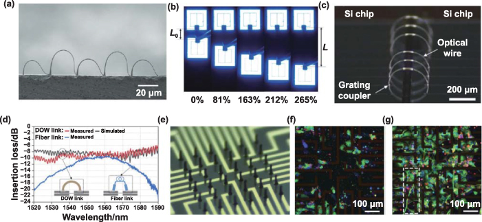
Figure 4. Meniscus-guided 3D printing of polymer composite for electrical and photonic applications. (a) Field emission scanning electron microscopy (FE-SEM) images of a series of 3D PEDOT:PSS microstructures. (b) Microscopic image of two LEDs under a 4.5 V bias and stretched by 0%–265%. Reprinted with permission from [60]. Copyright 2012 American Chemical Society. (c) Microscopic image of chip-to-chip connected optical wires. (d) Simulated and measured insertion losses of a directly bonded wire between grating couplers. Reprinted with permission from [68] © 2022 The Optical Society. (e) Printed 3D pillar (height = 80 ± 2 μm; diameter = 14 ± 1 μm) electrodes. (f) In situ immunophenotyping of 3D MEA-based cell-laden constructs on day 7 of human NSC differentiation without ES. The image was taken at the interface of the ventral surface of the construct and the Matrigel-coated insulating layer covering the Au electrodes and shows low-density human NSC-derived neurons (TUBB3+), related neurite formation, glial (GFAP+) cells, and underlying patterned Au electrodes as dark bands/silhouettes. (g) In situ immunophenotyping of 3D MEA-based cell-laden constructs on day 7 of human NSC differentiation including 3-day ES. [69] John Wiley & Sons.
Download figure:
Standard image High-resolution imageNumerous studies have focused on the printing of functional polymers. Because a meniscus can be as small as a few micrometers or even a few hundred nanometers, printed stimulus-responsive polymers can serve as micro/nanoscale sensors or actuators. Kim et al developed a high-resolution (250 nm) on-demand moisture sensor by exploiting the interferometric response of a 3D-printed PS nanoprobe (figure 5(a)) [70, 71]. Won et al used the meniscus-guided 3D printing method to form a stretchable poly(methyl methacrylate)/PPy gas sensor for NH3 (figure 5(b)) [72].

Figure 5. Meniscus-on-demand 3D printing of functional polymers. (a) Quantitative measurement of interferometric response of a nanoprobe to RH. Interference patterns at 30%–90% RH and the schematic illustration of a nanoprobe interferometer consisting of an RH-responsive polymer nanowire and a tapered optical fiber. Reprinted with permission from [70]. Copyright 2021 American Chemical Society. (b) Microarches of poly(methyl methacrylate)/PPy composite microtubes show robust sensitivities under different stretching conditions and no changes when exposed to 1 ppm NH3; inset: FE-SEM images of the microarch arrays. Reprinted from [72], Copyright 2017, with permission from Elsevier. (c) Azo-1 and a PS nanowire (500 nm [diameter] × 12.5 µm [length]) arms individually integrated onto the tip of a glass microcapillary tube. The optical microscope images show that the resulting tweezers successfully gripped a PS microparticle (d ∼ 4 µm) on a Si substrate upon UV irradiation (1.5 mW cm−2 for 20 s): 1 (contact) → 2 (gripping) → 3 (detachment); scale bar: 20 μm. Reproduced from [73] with permission from the Royal Society of Chemistry. (d) Schematic and optical micrograph of a four-segment PS/PEDOT:PSS bilayer with a straight shape at 20% and 50% RH. Reprinted with permission from [74]. Copyright 2021 American Chemical Society. (e) 3D-printed blue nanopixel series with controlled heights of 2, 4, 6, 8, and 10 μm. Each row contains a side-view optical bright-field (BF) image, a bottom-view optical BF image, and a bottom-view PL image. (f) Intensities and spot sizes of PL emissions of red nanopixels measured from a bottom-view PL image. Reprinted with permission from [76]. Copyright 2020 American Chemical Society. (g) Photograph of a nanowire photodetector (NWPD) array and a series of optical microscopy images showing degrees of stretching of up to 100%. [78] John Wiley & Sons.
Download figure:
Standard image High-resolution imageThe meniscus-guided 3D printing method can provide an effective route for manufacturing polymeric micro-actuators with programmable shapes and functions. Lee et al fabricated a light-driven supramolecular nanogripper (figure 5(c)) that could grip and release a 4 μm-diameter PS microparticle under ultraviolet (UV) stimulation [73]. Actuators with asymmetric structures (such as layered structures) can also be printed via meniscus guiding. Huan et al used a double-barrelled theta pipette as a nozzle for one-step 3D printing of programmable bilayer microscale structures (figure 5(d)). The bilayer was composed of PEDOT:PSS (the active layer) and PS (the passive layer) and was actuated by humidity and infrared light [74]. Similarly, Zhang et al fabricated a multilayer structure via meniscus-guided printing combined with localized electropolymerization [75] and thereby generated a microscale tweezer based on the opposite actuation behaviors of PPy:CF3SO3 and PEDOT:PSS under the same potential. Such meniscus-guided printed actuators respond to various stimuli (e.g. light, electric potential, humidity, and temperature) and so can be used to manipulate objects at the micro/nanoscale.
The addition of light-emitting agents, such as quantum dots, into optically transparent polymers can enable the direct printing of various optical functional devices. Bae et al 3D printed high-integration-density, high-brightness quantum dot–polystyrene color pixels with a lateral distance of only 620 nm and a pitch of 3 µm for red, green, and blue [76]. The light intensity of each 3D pixel could be controlled by the vertical pixel height, so that the pixels were brighter than 2D pixels (figures 5(e) and (f)). Furthermore, the nanoscale 3D pixels could be directly fabricated on rough substrates via meniscus-guided printing—even on the surface of photocopying paper [77]. Yoo et al printed oleic acid-capped PbS quantum dots, which were incorporated into poly(3-hexylthiopehene), and used these to develop high-performance, flexible, and stretchable UV–vis–near-infrared nanowire photodetectors (figure 5(g)). These could be stretched by as much as 100% and could be repeatedly used for up to 100 cycles [78].
3.3. Carbon nanomaterials
In recent years, carbon nanomaterials have been favored by researchers, due to their unique chemistry, electronic, optical, thermal, and mechanical properties [79–81]. Here, we review research progress on the meniscus-guided 3D printing of carbon nanomaterials and their potential applications.
Graphene is a 2D carbon nanomaterial comprising sp2-hybridized single-atom-thick carbon sheets [82, 83]. It is characterized by a low density, a high specific surface area, excellent mechanical properties, high conductivity, and stable chemical properties [84]. Graphene oxide (GO) is an important product of graphene [85]. Owing to the outstanding properties of GO, numerous studies have attempted to create 3D GO-based micro- and nanostructures [19, 86, 87]. GO is often converted to reduced graphene oxide (rGO) via chemical or thermal reduction, as rGO exhibits good electrical conductivity [88].
Kim et al were the first to report the meniscus-guided 3D printing of GO nanowires. At room temperature, a GO flake-dispersed aqueous ink meniscus was formed on a substrate via nanopipette–substrate contact. As the nanopipette was pulled up, the solvent evaporated rapidly, and the deposited solid matter gradually grew into a freestanding GO nanowire (figure 6(a)). The GO wire was then reduced to rGO via heat treatment or chemical treatment (using hydrazine). Several rGO nanostructures, including straight wires, bridges, suspended connections, and braided structures, were printed via this method (figure 6(b)). Moreover, the printed rGO structures could be successfully applied as electric interconnects and gas-sensing transducers (figure 6(c)) [32].
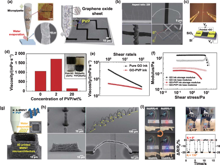
Figure 6. Meniscus-guided 3D printing of carbon nanomaterials for electrical applications. (a) Schematic of meniscus-on-demand 3D micro- and nanoprinting of GO nanowires. The left image is the pure GO ink printing process, and the right image is the GO-PVP composite-ink printing process. [32] John Wiley & Sons. Reprinted from [89], Copyright 2017, with permission from Elsevier. (b) FE-SEM images of 3D-printed rGO nanostructures: straight wires, a bridge, suspended connections, and braided structures. (Scale bar: 1 µm). [32] John Wiley & Sons. (c) Optical image of an rGO nanoarch between Au electrodes that functions as an electrical interconnect (top). Schematic of an rGO field-effect transistor with a Si/SiO2 substrate functioning as a gate dielectric and a back gate (bottom). [32] John Wiley & Sons. Reprinted from [89], Copyright 2017, with permission from Elsevier. (d) Histogram comparing the viscosities of the GO inks with 2 wt% GO and different PVP concentrations. The inset are optical images of the gel–sol transition of the inks with pure GO (left) and GO-20 wt% PVP (right). (e) and (f) Viscosity and storage and loss moduli as a function of shear rate and shear stress for pure GO and GO-PVP. Reprinted from [89], Copyright 2017, with permission from Elsevier. (g) Schematic of meniscus-on-demand 3D micro- and nanoprinting of an MWCNT/PVP microarchitecture. (h) FE-SEM images of MWCNT 3D-printed nanostructures: a pillar array, a freestanding bridge, a single wall, and a zigzag structure composed of 2D lines and 3D bridges on a curved substrate. Reprinted with permission from [92]. Copyright 2016 American Chemical Society. (i) Manufacturing of an MWCNT/PVP flexible strain sensor via meniscus-guided printing; the response of electrical resistance, △R/R0 to θf (bending degree of the forefinger) was stable. Reprinted with permission from [93]. Copyright 2018 American Chemical Society.
Download figure:
Standard image High-resolution imageTo improve the feasibility of printing multiple patterns, Chang et al optimized the rheological properties and concentration of a GO ink for a meniscus-guided printing process by adding polyvinylpyrrolidone (PVP) as a gelation inhibitor and rheology modifier. The interplanar distance between the GO sheets are increased by introducing excess PVP, thereby preventing the hydrogen-bonded-stacking of the GO sheets and causing slippage between the adjacent GO sheets, inducing the gel–sol transition of the inks. A histogram in figure 6(d) comparing the viscosities of the GO inks with 2 wt% GO and different PVP concentrations (0, 2, 20 wt%) clearly indicates the gel–sol transition upon the addition of 20 wt% PVP. In figures 6(e) and (f), the viscosity and modulus values as a function of the shear rate and shear stress for pure GO and GO-PVP inks are shown, which further confirms the gel–sol transition of the ink and its fluid-like behavior enabled by sufficient PVP content. Thus, the rheological property of the ink is effectively modified, and it can flow through a micronozzle without any applied pressure, enabling smooth and high-resolution printing of highly concentrated graphene patterns. And the ink was used to fabricate an rGO field-effect transistor (figure 6(c)) [89].
Carbon nanotubes are another attractive carbon nanomaterial [90, 91]. Kim et al reported the fabrication of highly conductive multi-walled carbon nanotube (MWCNT) microstructures via the meniscus-guided 3D printing method (figure 6(g)). An MWCNT suspension was mixed with 17 wt% PVP to obtain an ink with printing-compatible rheological properties. Using the developed method, a pillar array, a freestanding bridge, walls of various shapes, and a zigzag structure of MWCNTs were fabricated (figure 6(h)). The printed MWCNT structures demonstrated practical applicability as gas sensor transducers, point emitters, and radio-frequency inductors [92]. Furthermore, Wajahat et al fabricated an MWCNT/PVP flexible strain sensor via meniscus-guided printing (figure 6(i)) [93].
3.4. MOF
The Cambridge Structural Database currently contains 75 600 MOF structures [94]. MOFs are usually synthesized as powders, so they need to be shaped and densified into monoliths that can be easily handled and used in practical applications [95]. To achieve this, classical processes such as pelletization and extrusion involving mechanical forces or additives have been widely used [96–100]. However, these processes suffer from two longstanding challenges. First, shaping a monolith requires multiple, complex, and expensive machining processes. Second, the application of mechanical forces and additives significantly deteriorates the functional properties of MOFs, such as their porosity and surface area. For example, the application of mechanical forces can result in a loss of MOF crystallinity, and the addition of additives can result in insufficient MOF loading and block MOF pores [101]. Consequently, the porosity and surface area of MOF monoliths may be much lower than those of the corresponding crystalline MOF powders, and such MOF monoliths exhibit poor gas-uptake performance. Recently, 3D printing has emerged as an alternative shaping strategy for producing MOF monoliths [102–107], due to its cost-effectiveness and design flexibility in production. However, conventional 3D printing approaches also require the use of additives for shape retention, and the consequent pore blockage significantly deteriorates gas-uptake capability. In 2019, an innovative 3D printing strategy was reported that used MOF colloidal gels as inks without the need for additives, but the resulting structures' gas-adsorption properties, specifically their Brunauer–Emmett–Teller surface area, was lower than expected owing to insufficient crystallization [108, 109]. In 2022, Liu et al reported direct incorporation of evaporation-driven MOF nucleation and growth into a meniscus-guided process to produce a pure, freeform MOF micro-monolith (figure 7(a)), without the need for additives or mechanical forces. Figure 7(b) shows a pure HKUST-1 MOF microwall printed via a layer-by-layer meniscus-guided process. This printed monolith functioned as a micron-sized capacitive sensor of humidity (figures 7(c) and (d)) [21].
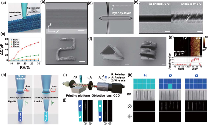
Figure 7. Meniscus on-demand 3D printing of MOFs and peptides. (a) Schematic of meniscus-guided 3D printing of an HKUST-1 microwall. (b) FE-SEM images of a 3D-printed HKUST-1 microwall (scale bar: 2 μm) and a serpentine wall (scale bar: 20 μm). (c) Plot of the capacitance change (ΔC) of printed HKUST-1 microwalls vs. RH. Reprinted with permission from [21]. Copyright 2022 American Chemical Society. (d) Optical micrograph images showing meniscus-guided layer-by-layer 3D printing of diphenylalanine (scale bar: 20 μm). (e) Bright-field transmission electron microscopy image of an as-printed and annealed FF line pattern (scale bar: 1 μm). (f) FE-SEM images of 3D-printed FF microstructures of a triangular prism (scale bar: 5 μm) and a perpentine wall (scale bar: 5 μm) (g) Vertical PFM images of an annealed FF layer under AC voltages of 0 and 10 V, respectively (scale bar: 1 μm). Reprinted with permission from [115]. Copyright 2021 American Chemical Society. (h) Schematic of 3D printing of crystalline FF at high RH and amorphous FF at low RH. (i) Schematic of in situ cross-polarized imaging of the 3D printing process. (j) Two heterojunction microwires consisting of amorphous and crystalline segments, and the corresponding cross-polarized images at θ = 45° and 90°. (k) Five freestanding encoded FF microwires demonstrating polarization-encoded anticounterfeiting properties. Reprinted with permission from [116]. Copyright 2022 American Chemical Society.
Download figure:
Standard image High-resolution image3.5. Peptides
Peptides have attracted significant interest owing to their programmable electrical, optical, and molecular recognition properties and biocompatibility [110]. Moreover, the self-assembling capacity of peptides, which is driven by weak non-covalent interactions, enables the spontaneous formation of micro- and nanostructures of various shapes, including spherical, rodlike, and tubular shapes, with superior crystallinity at the molecular level. However, the position and orientation of these micro/nano-assemblages is not controllable, limiting their practical application. Recently, 3D printing has been utilized to improve shaping during the fabrication of peptide-based materials through direct ink writing [111], inkjet printing [112], stereolithography [113], and digital light processing [114].
Yang et al developed a meniscus-guided 3D printing method for generating dipeptides with controlled shapes and crystallinity [115]. This method consists of two steps: (i) meniscus-guided layer-by-layer solidification of dipeptides (figure 7(e)), and (ii) post-thermal annealing to achieve molecular crystallization. Various self-assembled 3D peptide structures were printed, including a two-step microwall, a triangular prism, and a zigzag wall (figure 7(f)). An annealed printed structure showed a vertical piezo-response property (figure 7(g)) and thus potential applications in electronics.
In another study, dipeptide crystallization was modulated in situ during a meniscus-guided 3D printing process (figure 7(h)) [116]. Specifically, the self-assembly-based crystallization of dipeptides was switched on and off by altering the RH during the printing process to control the evaporation of the binary solvent. This method allowed control of the transition of diphenylalanine (FF) from its crystalline form to its amorphous form, and the printed structure exhibited the anisotropy of refractive index (figure 7(i)). Figures 7(j) and (k) show polarization-encoded 3D anticounterfeiting labels containing a combination of amorphous and crystalline encoded segments.
3.6. Metal halide perovskites
Over the past decades, metal halide perovskites have emerged as outstanding optoelectronic and photonic materials owing to their exceptional properties, such as their high strength, tunable photoluminescence (PL), large optical absorption, high carrier mobility, and facile solution-processability [117–121]. The utilization of metal halide perovskites for diverse applications has thus been extensively investigated. Jeong et al demonstrated the application of metal halide perovskites as solar cells and achieved a record-breaking power conversion efficiency (25.6%) [122], and Kim et al demonstrated their application in LEDs that exhibited an external quantum efficiency of 28.9% [123]. This illustrates the excellent optoelectronic performance and potential of the metal halide perovskites.
Additionally, owing to the urgent demand for optoelectronics devices with high integration density, numerous integrated functional devices with micro/nanostructures have been developed, such as metal halide perovskite micro–nano lasers [124, 125]and metal halide perovskite nanowire array photodetectors [126]. However, these metal halide perovskite devices are fabricated using conventional methods, such as electron beam lithography, photolithography, and nanoimprinting [127, 128], which are costly and time consuming.
Therefore, Chen et al developed a meniscus-guided 3D printing method that employs metal halide perovskites [20]. The metal-halide-perovskite precursor ink underwent crystallization at a confined femtoliter ink meniscus, and the sub-micro scale 3D printing was enabled by the continuous withdrawal of the micropipette from the substrate (figures 8(a) and (b)). The nucleation and growth mechanisms of metal halide perovskite crystals were revealed by calculating the concentration field of metal halide perovskite solutes inside the meniscus. The mechanisms theoretically demonstrate the origin of the tubular structure. Additionally, a metal halide perovskite sub-micro wire fabricated via meniscus-guided printing featured a well-oriented crystalline structure, which proved the usefulness of meniscus-guided printing for fabricating these crystalline structures.

Figure 8. Meniscus-on-demand 3D printing of metal halide perovskites for electrical and photonic devices. (a) Schematic of meniscus-guided 3D printing of organic–inorganic metal halide perovskites. Inset: evaporative loss of solvent at the meniscus surface, and computed concentration of perovskite solutes inside the meniscus (height = 250 nm; wetting diameter = 1160 nm), exhibiting a rim-shaped concentration field. [20] John Wiley & Sons. (b) Optical microscopy images showing the results of meniscus-guided 3D printing. Reprinted with permission from [129]. Copyright 2021 American Chemical Society. (c) FE-SEM image of a freestanding perovskite sub-micro wire with a high aspect ratio (>30) (scale bar: 1 µm). (d) Tilted perovskite sub-micro wires fabricated at various pipette–substrate angles, θ (scale bar: 5 µm), and a tilted serpentine structure (scale bar: 2 µm). [20] John Wiley & Sons. (e) FE-SEM image of an as-printed perovskite RGB tri-pixel consisting of CH3NH3PbI3 (R: left), CH3NH3PbBr3 (G: middle), and CH3NH3Cl3 (B: right) sub-micro pillars; corresponding side-view optical photoluminescence image of RGB tri-pixels. (f) PL image of a 'smiley face' sub-micro pixel matrix. (g) 3D-printed sub-micro-pixel-based multilevel anticounterfeiting applications. Reprinted with permission from [129]. Copyright 2021 American Chemical Society. (h) 3D-printed perovskite sub-microwire-based photodetector (scale bar: 50 µm), and its photocurrent–time trace. [20] John Wiley & Sons.
Download figure:
Standard image High-resolution image
Various metal halide perovskite micro/nanostructures can be obtained via meniscus-guided printing (figures 8(c)–(f)), including high-aspect-ratio sub-micro pillars, tilted sub-micro wires, serpentine structures, and sub-micro pixels, which have many photonic and electronics applications. Chen et al showed that the brightness of a high-resolution display device could be improved by increasing pixel height (figures 8(f) and (g)) [129], which enabled them to develop a multilevel, high-resolution anticounterfeiting security label. Moreover, the sub-micro wire height, which is inaccessible by conventional wide-field microscopes, may be capable of encoding data. In addition, the freestanding metal halide perovskite sub-micro wire heterostructures with high control over shape and composition are fabricated using the same printing protocol [130]. In terms of electrical applications, a metal halide perovskite sub-micro bridge between two Pt electrodes was fabricated as a photodetector through meniscus-guided printing, and the system exhibited switching behavior when the middle of the sub-micro bridge was subjected to laser illumination (figure 8(h)) [20].
The above-described studies have shown that meniscus-on-demand printing allows the fabrication of freeform metal halide perovskite micro/nanostructures with high reproducibility. Thus, this printing method could serve as a good platform for developing advanced metal halide perovskite-based electronic and photonic devices.
4. Challenges and prospects
In this review, we have shown that the meniscus-on-demand 3D printing method can be applied at the microscale and nanoscale to form diverse and advanced electronic and photonic devices from various materials, such as polymers, metal, and metal halide perovskites. However, despite the great developments in the meniscus-on-demand printing field, some longstanding problems remain to be solved. First, new inks applicable to meniscus-on-demand printing should be developed, to allow for the fabrication of practical multifunctional devices. Additionally, the fundamental mechanisms of different aspects of the meniscus-guided printing process, including meniscus formation during multi-nozzle parallel printing, the relationships between ink rheology and printability, and the achievable potential best resolution with a nanoscale meniscus, need to be understood. Furthermore, meniscus-on-demand printing should be integrated with other conventional printing techniques, such as EHD printing, inkjet printing, and nanoimprinting, to realize novel capabilities that are only obtainable using such hybrid approaches. This area remains largely unexplored. Finally, standardized printing systems, such as robust printer-nozzle systems, precise controlling units, and imaging systems, should be developed to enable high-resolution, high-output practical applications.
5. Conclusion
This review presented recent advances in meniscus-on-demand 3D micro- and nanoprinting by examining the diverse types of ink materials that have been used and the potential applications of these printing methods in several fields, including electronics and photonics. And a summary table for the printing mechanism and resolution for different materials is shown in table 1. The advantages of meniscus-on-demand 3D printing were emphasized, including its high resolution, tolerance of various materials, and enabling controllable formation of individual structures. Moreover, the wide applicability of meniscus-on-demand 3D-printed structures was described, such as in the manufacturing of electronic circuits, sensing devices, and photonic devices. The current challenges and prospects of meniscus-on-demand 3D printing were also outlined, to stimulate its further development. Clearly, meniscus-on-demand 3D printing has the potential to be a leading platform for the additive manufacturing of high-resolution functional devices.
Table 1. Summary of printing materials, mechanisms, and precisions for meniscus-on-demand 3D printing.
| Category | Ink materials | Printing mechanisms | Printing resolution | References |
|---|---|---|---|---|
| Metal | Nanoparticle (Ag, Au) | Nanoparticle assembly | ∼5 µm | [29, 51–53] |
| Electrolyte solution | Electrodeposition | ∼200 nm | [18, 23, 30, 43–50] | |
| Liquid metal | Solidification | ∼150 µm | [27–29] | |
| Polymers | PPy | Oxidative polymerization | ∼50 nm | [17, 26, 59, 60, 72, 75] |
| PEDOT:PSS | Solidification | ∼2 µm | [60, 61, 69, 74, 75] | |
| PANI | Electropolymerization | ∼500 nm | [62] | |
| PS | Solidification | ∼2 µm | [63, 70, 71, 73, 76] | |
| Carbon-based | Graphene oxide | Solidification | ∼800 nm | [32, 89] |
| Carbon nanotube | Solidification | ∼8 µm | [92, 93] | |
| MOF | HKUST-1 | Crystallization | ∼3 µm | [21] |
| Peptides | Dipeptides | Molecular assembly | ∼2 µm | [115, 116] |
| Perovskites | MAPbX3 | Crystallization | ∼600 nm | [20, 129, 130] |
Acknowledgments
This work was supported by the General Research Fund (17200222, 17208919, 17204020) of the Research Grants Council of Hong Kong; the National Natural Science Foundation of China/Research Grants Council Joint Research Scheme (N_HKU743/22); the Seed Fund for Basic Research (201910159047, 202111159097) of the University Research Committee (URC), The University of Hong Kong.