


Abstract
Roll-to-roll printing provides an efficient way to fabricate large quantities of flexible electronic devices at low cost. However, building a single multilayered electronic device such as a diode requires precise layer-to-layer alignment, which is currently a major technical challenge for roll-to-roll printing. Here, we report a novel self-aligned strategy to fabricate fully printed organic Schottky diodes on pre-patterned plastic substrates. This strategy utilizes imprinted networks of capillary channels to guide the flow of inks delivered sequentially into adjoining ink receivers by inkjet printing, allowing self-alignment at the micrometer level. The optimized design of the capillary channels and ink receivers realized better control of ink flows and significantly improved device yield. Printed diodes exhibited outstanding rectification ratios (>104) and excellent stability against repeated bending. Our work demonstrates a promising method for large-scale manufacturing of flexible and printed diodes.
Export citation and abstract BibTeX RIS
1. Introduction
With the impending development of the Internet of things (IOT) [1] and wearable technology [2, 3], the consumer electronics market is subject to enhanced demand for flexible circuits. Printing of electronic inks is regarded as a promising route to realize low-cost, high-throughput manufacturing of flexible electronic devices for a variety of novel applications, including smart labels [4, 5], wearable sensors [6], displays [7, 8] and flexible batteries [9, 10]. Roll-to-roll (R2R) printing, in particular, can significantly improve the throughput and further reduce production costs [11–13]. Although several printing techniques, such as inkjet printing, aerosol jet printing and gravure printing, are compatible with roll-to-roll processing, there are several key technical challenges when making flexible circuits with excellent electrical performance and high yield by roll-to-roll printing. First, patterning small features less than 10 μm is a technical challenge for printed electronics. Improving printing resolution is important for reducing the overall device footprint and increasing packing density. The resolution of printing is greatly influenced by the printing methods and substrate conditions [14]. Wu et al reduced the smallest feature size in inkjet printing down to <10 μm by improving the wave generator of an electrohydrodynamic printer [15]. Sele et al utilized surface modification to control the motion of the receding contact line of the ink drop, resulting in a gap less than 100 nm between two printed electrodes [16]. Using flexographic printing, Twoley et al reported printed patterns with a line width of 6.35 μm [17]. Although printed features with high resolution have been demonstrated, creating narrow conductive lines with high aspect ratio and crisp edges still remains a challenge due to the ink spreading on the substrate. Materials registration is another significant challenge when building multi-layer devices by printing on a moving web. Misalignment of different material layers may degrade device performance or cause electrical shorts. Chang et al developed a R2R web handling system and a reverse offset printing process, which has an overlay of ±5 μm between two 500 mm wide films [18]. Cao et al realized self-alignment between different layers in a transistor by chemically modifying the surface of the existing layers to control the wetting of the ink printed on the top [19]. However, a reliable roll-to-roll printing process requires solving the resolution and alignment issues at the same time, which requires alignment of the subsequent layer to a patterned small feature at micrometer-level on a moving flexible substrate [20]. These two challenges limit the industrial application of roll-to-roll printing.
To address these two challenges at the same time, a novel method termed SCALE (Self-aligned, Capillarity-Assisted Lithography for Electronics) has been developed to fabricate multiple components of integrated circuits [20–23]. SCALE utilizes micro-imprinting to create a complex network of circular ink receivers and small capillary channels on the top surface of a plastic substrate. Because of its non-contact and digital nature, inkjet printing [24–26] is ideally suited to print on these patterned substrates. When inks are printed into the receivers by a drop-on-demand inkjet printhead, they spontaneously flow under capillary forces into all the capillary channels connected to the receivers. Film deposition occurs upon drying of the inks. Different films can be layered on top of one another by delivering each ink sequentially into receivers with overlapping ink receivers or capillary channels, as we will illustrate below. Compared with other existing solutions of the resolution and registration problems, the advantages of SCALE process are: (i) Deep capillary channels help preventing the spreading of inks on the substrate, resulting in high aspect-ratio conductive lines with clearly defined edges [27]; (ii) Since receivers have diameters on the order of 100 μm, the precision required to deliver ink is substantially relaxed. Consequently, this process is more suitable for printing on a moving web and more compatible with high-throughput, roll-to-roll processing. A variety of printed circuit elements fabricated via the SCALE strategy have been reported to have good electrical performance, including transistors [20, 22, 28, 29], resistors [20, 30] and capacitors [20, 31]. However, a multilayer device with a stacked structure such as a diode has been hard to achieve using the SCALE process [29].
Diodes are ubiquitous elements in electronic circuits that can be used in a vast range of applications, including radio frequency identification (RFID) tags [32], energy harvesting devices [33] and wireless communication [34]. Organic Schottky diodes based on polymer semiconductors have attracted considerable attention in the printed electronics field due to the relatively simple device structure compared to a PN junction diode [35–38]. A typical printed organic Schottky diode consists of a semiconductor thin film sandwiched between two electrode layers forming one ohmic contact and one Schottky contact depending on the work function of the electrodes. A diode conducts appreciable current only in one direction due to the existence of the asymmetric energy barrier at the Schottky contact. Printing is regarded as a very promising way to make diodes in large quantities [39], and several reports have appeared on printed diodes [33, 37, 40–46], which are summarized in table 1. However, most of the fabrication processes include one or more steps that are not compatible with large-scale roll-to-roll printing. For example, the bottom or top electrodes of the printed diodes are deposited or patterned using traditional non-printing approaches [33, 37, 41, 42, 44, 47], or an additional bonding step is required to connect the diode to other devices in the circuit [40]. Fully printed diodes in a roll-to-roll compatible process are much less frequently reported [45, 48]. Finding a reliable process to fabricate fully printed diodes in large quantities still remains a challenge.
Table 1. Comparison of the results of this work with literature results.
| Semiconductor materials | Fabrication methods | Rectification ratio | Active area | Frequency | References |
|---|---|---|---|---|---|
| P3HT | SCALE | 5 × 10⁴ | 0.196 mm2 | 100 kHz | This work |
| Si and NbSi2 particles | Screen printing and evaporation | 10 | 0.05 mm2 | 1.6 GHz | [33] |
| PTAA (poly(triaryl amine)) | Gravure printing and sputtering | 1 × 10⁴ | 4 mm2 | 10 MHz | [37] |
| PTAA | Inkjet printing | 1 × 10⁴ | 9 mm2 | N/A | [40] |
| IGZO (indium galium zinc oxide) | Gravure printing and lamination | 1 × 10⁵ | N/A | 13.56 MHz | [41] |
| PTAA | Gravure printing and evaporation | N/A | N/A | 13.56 MHz | [42] |
| PTAA | Gravure printing and evaporation | 1 × 10³ | 0.2 mm2 | 13.56 MHz | [47] |
| CN-PPV (Poly[2-methoxy-5-(2-ethylhexyloxy)-1,4-(1-cyano-vinylene) phenylene])/PPy and CN-PPV/PEDOT | Inkjet printing (ITO glass as the substrate) | 117 | 0.45 mm2 | N/A | [44] |
| PTAA | Inkjet printing | 200 | 9 mm2 | N/A | [45] |
A vertically stacked structure is preferred for printed diodes due to the larger contact area between the metals and the semiconductor, which leads to larger forward-bias currents than a horizontal, coplanar structure. The challenging part of making printed diodes in a vertically stacked structure via the SCALE process lies in preventing a short between the top and bottom electrodes. This is because in such structures the semiconductor layers are thin and can have pinholes. An additional complication that can lead to shorting is uncontrolled spreading of ink into channels or cavities that have already received ink or that are intended to be devoid of ink, as will be clarified below.
Here we report a roll-to-roll compatible printing method to fabricate self-aligned, fully printed diodes on plastic substrates using SCALE. The diode is based on a Ag/P3HT(poly(3-hexylthiophene))/PEDOT:PSS(poly(3,4-ethylenedioxythiophene) polystyrene sulfonate) vertical stack. An Ag thin film serves as the bottom electrode, forming a Schottky contact with the P3HT semiconducting layer on top of it. PEDOT:PSS is chosen as the top electrode material since it forms an ohmic contact with the P3HT layer. The capillary network design of the diode includes several flow control structures to achieve precise ink flow, which is a key point to avoid electrical shorts and to improve device performance. Employing this new strategy, we have achieved fully printed diodes on polyethylene terephthalate (PET) with rectification ratios up to 5 × 10⁴. The results of bending tests indicate excellent mechanical durability of the printed diodes. Overall, it appears promising to scale-up the whole fabrication process to roll-to-roll printing in order to facilitate low-cost, large scale manufacturing of printed diodes.
2. Experimental section
2.1. Silicon master template
The silicon master template was prepared by three cycles of photolithography and dry etching on a 4-in silicon wafer in order to take advantage of the high resolution of traditional patterning methods (figure S1 is available online at stacks.iop.org/FPE/5/015006/mmedia). In this paper, a contact receiver is defined as a circular depression where inks are delivered in order to form an external contact pad for a device; a device receiver is a circular cavity in which the delivered ink dries and forms an active layer of a device. (1) In the first patterning cycle, the receiver pattern shared by the semiconductor layer and the top electrode was created on the silicon wafer. A silicon wafer was dried at >100 °C on a hot plate and then immersed in a hexamethyldisilazane (HMDS) atmosphere. A layer of positive photoresist (Microposit S1813) was deposited onto the wafer by spin-coating at 2000 rpm for 30 s followed by soft-baking at 115 °C for 1 min. The wafer was then exposed to ultraviolet light for 6 s in a photo aligner under a photomask and immersed in a diluted solution of developer (Microposit 351 (Dow): H2O = 1:5 by volume) for 40 s to remove the photoresist in the exposed area. A plasma etcher (STS) was used to etch the exposed area down to a depth of 4 μm. The wafer was then washed by acetone, methanol, and isopropyl alcohol in sequence to strip off the photoresist. (2) The second patterning cycle created the ink receiver and the capillary channel for the bottom Ag electrode. The silicon wafer from the last step was heated at 200 °C for 5 min and treated in a HMDS atmosphere again. Then, a layer of positive photoresist (AZ9260, MicroChemicals) was spin-coated onto the wafer (300 rpm for 10 s then 2000 rpm for 60 s) to achieve a thickness of about 10 μm. After pre-baking at 110 °C for 165 s, the wafer was aligned to the photomask for the second layer in the same photo aligner and exposed to UV light for 42 s. The wafer was then washed in a mixture of AZ400K (Merck Performance Materials) and H2O (AZ400K:H2O = 1:4) for 4 min to remove the exposed part of the photoresist. The exposed area of the silicon wafer was then dry etched to a depth of 5 μm by the plasma etcher (STS). To remove the rest of the AZ 9260 photoresist layer, the wafer was immersed in heated 1165 resist remover (Dow) for 1 h. (3) In the third cycle, the receivers and capillary channels designed to connect this single diode to other devices were patterned using a similar procedure as the second cycle except for the etching step. A plasma deep trench etcher (SLR 770) was employed instead of the STS etcher in the third cycle to obtain indented features with vertical walls and a depth of 10 μm. The wafer was further cleaned in a Piranha solution (H2SO4 and H2O2, 1:1; WARNING: Piranha solution is highly oxidizing and corrosive!!) to dissolve any residual photoresist.
2.2. Imprinted flexible substrates
The patterns on the silicon master template were first transferred to a flexible PDMS (polydimethylsiloxane) stamp. The wafer was pre-treated in a trichloro(1 H, 1 H, 2 H, 2 H-perfluorooctyl)silane vapor to facilitate the peeling off process of the PDMS stamp. The PDMS elastomer and the curing agent (Sylgard 184, Dow Corning) were mixed to a weight ratio of 10:1 and the mixture was poured slowly on top of the silicon master template. Then the PDMS was heated to 70 °C in an oven and kept at that temperature for 1 h. After the PDMS layer was fully cured and solidified, it was peeled from the silicon template followed by a post-annealing at 100 °C for 30 min in an oven.
A PET sheet was pre-cleaned by isopropyl alcohol. A layer of UV-crosslinkable imprint resist (NOA73: Norland Optical Adhesive 73) was drop-casted onto the PET sheet (figure S2). Then the PDMS stamp was pressed into the imprint resist, which was illuminated by an ultra-violet light for 2 h. After the imprint resist solidified, it adhered firmly to the PET sheet. The PDMS stamp was then delaminated from the imprint resist, resulting in pattern transfer. The imprinted NOA73-PET laminate served as the substrate for printing devices. The thickness of the imprint resist after UV curing is about 25 μm.
2.3. Ink preparation and inkjet printing of diodes
The particle-free Ag ink (EI-011) was purchased from Electroninks. The P3HT ink was prepared by dissolving P3HT (regioregular, Sigma-Aldrich) in dichlorobenzene to various concentrations (25, 37.5 and 50 mg ml−1). The PEDOT:PSS ink was prepared by mixing a commercial PEDOT:PSS ink (PH1000, Heraeus) with ethylene glycol (6 wt%) to improve the conductivity [49].
All the inks were inkjet printed using an inkjet nozzle (Microfab) with an 80 μm orifice in ambient air, according to the sequence shown in figure 1. A particle-free Ag ink (Electroninks, Inc.) was first printed into two recievers (figure 1(b)) and annealed at 100 °C for 3 min on a hotplate. Then P3HT ink was deposited on top of the Ag film in the device reciever (figure 1(c)) and heated at 120 °C for 30 min in a N2 atmosphere in a glovebox. Then the particle-free Ag ink was delivered into the side, contact receiver to form the connection to the top electrode (figure 1(d)) and dried. Finally, the top electrode was printed using the PEDOT:PSS ink (figure 1(e)) and annealed at 120 °C for 10 min in a glovebox.
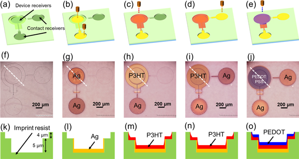
Figure 1. Schematic illustration of the printing process of a diode using the SCALE process showing (a) the as-prepared imprinted substrate, (b) Ag electrode printing, (c) P3HT ink printing, (d) side Ag electrode printing and (e) top PEDOT:PSS electrode printing with the corresponding top view optical images (f)–(j), and the schematic cross sections (k)–(o) along the white dashed line.
Download figure:
Standard image High-resolution image2.4. Characterization
Optical images were taken with a Hirox high-resolution optical microscope. All the SEM images were taken with a JEOL 6500 scanning electron microscope (SEM). The current–voltage (I–V) curves were measured at a probe station with Keithley 236 and 237 source meters. A signal generator (Agilent 33512B) was utilized to apply the sine waves to the diodes, and an oscilloscope (Tektronix TDS3014C) was employed to measure the input and output signals.
3. Results and discussion
Figure 1 shows an overview of the printing process for diodes via the SCALE strategy. For example, figures 1(a), (f) and (k) display the 3D schematic, the corresponding top view optical image of an imprinted pattern, and the device cross-section along the dotted line. The preparation process of the imprinted substrates is discussed in detail in the supporting information (figures S1 and S2). The diode was mainly constructed within the two concentric device receivers shown on the upper left corner of figures 1(a)–(j). The smaller receiver (diameter = 500 μm, depth = 5 μm) for the bottom Ag electrode was depressed within the larger receiver (diameter = 700 μm, depth = 4 μm) designed for the semiconductor and the top electrode. The other two contact receivers and the capillary channels connected to them served as the external connection to the bottom and top electrodes, so the diode could be integrated into a circuit. The depth of these contact receivers and the capillary channels was 10 μm because a larger depth facilitates a longer capillary flow distance, which is preferrable for external connections.
The printing process is depicted schematically in figures 1(b)–(e). First, a particle-free Ag ink was delivered into the device receiver and contact receiver (figures 1(b), (g), (l)). The device receiver and contact receiver were connected through a capillary channel (width = 10–30 μm) with a two-tier junction, whose structure and function are discussed later. The depth difference between the Ag device receiver (5 μm) and the Ag contact receiver (10 μm) resulted in a thicker Ag film in the contact receiver after annealing. So, the contact receiver is less transparent and looks darker than the device receiver. In the next step, P3HT ink was printed into the larger device receiver over the Ag film (figure 1(c)) and the ink flowed into a wide channel (width = 100 μm) to fully cover the underlying Ag film (figures 1(h), (m)). After drying and annealing of the P3HT film, the same particle-free Ag ink was printed into the contact receiver on the right side (figure 1(d)). The adjoining capillary channel that connected to the P3HT-filled device receiver contained a two-tier junction. Thus, Ag ink could flow via the channel onto the circular P3HT film and form a crescent-shaped contact along the circular ink receiver lip (figure 1(i)). Lastly, PEDOT:PSS ink was printed into the same receiver as the P3HT ink (figures 1(e), (j), (o)). The PEDOT:PSS also covered the crescent-shaped Ag film on top of P3HT to make an external connection to the top electrode (figure 1(j)).
To fabricate a diode in a vertically stacked structure using the SCALE process, precise control of the ink flow in the imprinted capillary network is critical to avoid short circuits and to improve reproducibility. We incorporated two types of ink flow control structures, namely flow stoppers and microfluidic diodes, into the capillary network to regulate ink flows and subsequent film deposition. Figure 2(a) shows the flow control structures in two regions of interest in a schematic drawing of a printed diode from top view. Figure 2(b) displays the corresponding top view optical image. Enlarged optical images of Region 1 are shown in figures 2(c), (d) to show the design details clearly. Region 2 is shown in figure 3 and will be discussed later.

Figure 2. Optical and SEM images of an unfinished diode showing details of the microfluidic diodes and the flow stoppers. (a) A top view scheme and (b) an optical image of a partially completed printed diode. Two regions of interest are highlighted. (c), (d) Enlarged optical images for Region 1 after depositing the Ag film (c) and the P3HT film (d). (e), (f) Slightly tilted SEM images for the red dotted regions in (c) and (d), correspondingly.
Download figure:
Standard image High-resolution image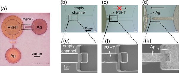
Figure 3. Role of microfluidic diode in Region 2. (a) Optical image of a partially completed printed diode showing the second microfluidic diode in Region 2. (b–d) Zoom in optical images of Region 2 showing (b) the empty channels, (c) the pinning effect of P3HT ink and (d) the formation of the crescent shaped Ag film. (e–g) corresponding tilted SEM images of the black dotted boxes in (b–d).
Download figure:
Standard image High-resolution image
Figure 4. (a)–(c) top view optical images of annealed P3HT films deposited using inks with a P3HT concentration of (a) 25 mg ml−1, (b) 37.5 mg ml−1 and (c) 50 mg ml−1. (d)–(f) Cross-sectional SEM images for completed devices taken along the red dashed lines shown in (a)–(c).
Download figure:
Standard image High-resolution imageA flow stopper is a rectangular depression [29]. Two stoppers were introduced along the wide channel connected to the P3HT receiver (figures 2(c), (d)). The stoppers (depth = 10 μm) were deeper than the wide P3HT channel (depth = 4 μm), thus creating an edge along the flow path of the Ag ink and obstructing further flow along the side walls of the wide channel. When the Ag ink was delivered to the contact receiver at the bottom of the image, the ink passed the microfluidic diode, bifurcated along the walls on both sides at the intersection of the wide P3HT channel and the narrow channel and then was stopped by the rectangular depressions due to contact line pinning at the sharp edge. Without the stoppers, the Ag ink might flow along the side walls of the wide P3HT channel and into the adjoining P3HT receiver, in which the Ag film along the side wall could not be fully covered by the P3HT film. Since PEDOT:PSS shared the device receiver with P3HT, the uncovered Ag film along the side wall would be in contact with the PEDOT:PSS layer, causing shorting defects.
The second type of ink flow control structures was the microfluidic diode. A microfluidic diode consists of two adjoining open capillary channels: a narrow, shallow channel abutting a wide, deep channel (figures 2(e), (f)). This junction provides unidirectional ink transport that only allows the ink to flow from the deeper channel to the shallower one but halts the flow in the opposite direction due to the Gibbs criterion that governs flow over edges and steps [50]. The microfluidic diode in Region 1 is displayed in figures 2(c), (d) marked by red dotted boxes. Ag ink delivered to the contact receiver flowed through the junction to make connection to the Ag delivered nearly simultaneously to the device receiver. A granular Ag film was deposited uniformly in the microfluidic diode and in the two receivers. The tilted SEM image in figure 2(e) shows the high quality Ag film in the microfluidic diode. In the next step, P3HT ink was delivered to the device receiver, covering the bottom Ag electrode. Excess P3HT ink flowed out of the receiver and down the capillary, but was pinned at the junction (figure 2(d)). The SEM image in figure 2(f) clearly shows that the deposition of P3HT stopped at the junction. Interestingly, this also indicates that the underlying Ag film does not disturb the flow control function of the microfluidic diode. Crucially, the microfluidic diode prevented the P3HT ink from flowing over the Ag contact pad, which is important for clear device definition and integration into circuits.
Figure 3(a) shows the microfluidic diode in Region 2 on the right side of the device in the black dotted box. Figures 3(b)–(d) display the top view optical images of the junction before printing, after P3HT deposition, and after the second Ag deposition, respectively. Excess P3HT ink delivered to the device receiver (as described above) flowed into the narrow capillary but stopped precisely at the junction (figures 3(c), (f)). After the P3HT film dried, the Ag ink delivered subsequently to the contact receiver on the right flowed through the junction over the P3HT film in the narrow channel and into the circular lip on the right side of the device receiver. The deposited Ag film formed a crescent shape on the lip because the hydrophobicity of the P3HT surface inhibited the ink from flowing and spreading farther. Thus, this second microfluidic diode blocked P3HT ink from flowing over the external contact but then allowed the Ag ink to pass the junction to add the necessary connection to the top device electrode, namely PEDOT, delivered to the device receiver at the last step (see figure 1(e)). PEDOT:PSS ink has a higher surface tension than Ag and P3HT ink [50]. So, the PEDOT:PSS ink was confined within its receiver very well and did not enter the adjacent narrow capillary channels filled with Ag (and partially with P3HT). Taking advantage of the difference of surface tension of the inks prevents undesirable contact between the top and bottom electrodes. This is one reason why PEDOT:PSS was placed on the top instead of at the bottom.
The thickness of the P3HT film has a significant influence on the device performance and yield. Figure 4 shows the P3HT film deposited from inks with concentrations varied from 25 mg ml−1 to 50 mg ml−1. Figures 4(a)–(c) show the top view optical images of the P3HT film over the bottom Ag electrode. To characterize the thickness of P3HT films, completed devices were cut across the P3HT receivers along the red dashed lines after printing the top PEDOT:PSS electrodes. Cross-sectional SEM images taken at the center point of the P3HT receiver are shown in figures 4(d)–(f). When a 25 mg ml−1 P3HT ink was used, the underlying Ag film was not fully covered by the P3HT film. Most of P3HT deposited along the edge because the ink wet the sidewalls of the receiver, leaving a thin and non-uniform P3HT film covering the Ag electrode in the center. A P3HT layer is barely visible between the Ag and PEDOT:PSS films in figure 4(d). As a result, all devices fabricated with 25 mg ml−1 P3HT inks were shorted, indicating that this concentration was too low to deposit a thick enough P3HT film. When the ink concentration increased to 37.5 mg ml−1, the Ag electrode was fully covered by a P3HT film with a thickness of 528 nm at the center. The yield of functional diodes printed with the 37.5 mg ml−1 P3HT ink was around 22%, which was not satisfactory for a reliable process. When a P3HT ink of 50 mg ml−1 was used, the film thickness at the center of the device receiver increased to 950 nm, resulting in a raised yield up to 90%. The boost in yield upon increasing ink concentration could be explained by the thinning of the P3HT film at the edge of the Ag-coated device receiver, see figure 1(n). The P3HT film covering the vertical wall at the edge of the device receiver was much thinner than the P3HT film over the center of the receiver. Using a P3HT ink with a concentration of 37.5 mg ml−1 had a higher possibility of leaving a P3HT film that was too thin at the edge of the receiver to cover the underlying Ag film, leading pinholes and shorts. Consequently, P3HT inks with a concentration of 50 mg ml−1 were used for diode printing and further device tests. The humidity when printing the diodes was also critical to the yield; high humidity led to undesirable wetting of the P3HT ink outside the device receiver, resulting in a thinner P3HT film in the device receiver. A relative humidity around 20% was needed to guarantee a high yield.
Figure 5 presents the electrical performance of printed diodes using P3HT inks with a concentration of 50 mg ml−1. Figure 5(a) plots the I–V characteristic of a printed diode when sweeping the voltage applied to the top PEDOT:PSS electrode from −1 V to 1 V and grounding the bottom Ag electrode. No measurable hysteresis was observed. Figure 5(b) overlays the I–V curves of 25 printed diodes to evaluate the reproducibility of the process, and the calculated rectification ratios were measured to be 103.5±0.6, which is summarized in a histogram (figure 5(c)). The variation in device performance could be further improved by better control of the ink delivery process and the substrate wetting condition.
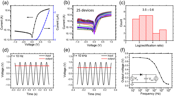
Figure 5. Static and dynamic electrical performances of printed diodes (a) IV characteristic of a printed diode. (b) IV curves collected from 25 printed diodes and (c) histogram of log(rectification ratio) of these devices. (d) Dynamic performance of a rectifier circuit (shown in the inset image in (f)) at an input frequency of (d) 10 Hz and (e) 10 kHz. (f) Output voltage as a function of input frequency for the rectifier circuit in the inset image. The capacitor connected in series with the diode is 1 μF.
Download figure:
Standard image High-resolution imageIn order to assess the printed diode as a rectifier, a simple circuit was employed for dynamic measurements in which a printed diode was connected in series with a commercial capacitor (C = 1 μF). The measurement circuit is shown in the inset plot in figure 5(f). Under a 10 Hz, 1 V peak-to-peak oscillating input signal, an output DC voltage of 0.7 V was obtained (figure 5(d)), which demonstrates a maximum 70% rectification efficiency. A DC output voltage of 0.55 V was maintained when the input frequency rose to 10 kHz without any AC ripples (figure 5(e)). The frequency response of the output of the rectifier circuit is plotted in figure 5(f), indicating that the printed diodes rectified an AC signal with a frequency as high as 100 kHz. The operating frequency of the printed diode by SCALE is relatively lower compared with best results in literature [33]. The dynamic performance can be improved by optimizing the device design to reduce the thickness of the semiconductor layer or by utilizing inorganic semiconductor materials with higher intrinsic mobility.
As shown in figure 6(a), an array of diodes was printed on a flexible substrate. The mechanical durability of the printed diodes was investigated by measuring the I–V characteristics under various bending conditions, as shown schematically in figure 6(b). The device was first tested in situ when wrapped around a glass vial with a bending radius of 1.25 or 1 cm, which correspond to a tensile strain of 0.64% or 0.8%. The electrical performance was unchanged under a tensile strain up to 0.8% (figure 6(c)). Then the device was bent repeatedly over a glass vial to a tensile strain of 0.8% and the electrical performance was tracked, figure 6(d). After 5000 bend cycles, there were no appreciable changes in the electrical performance, demonstrating excellent mechanical durability. Printed P3HT and PEDOT:PSS films are inherently flexible, but it was easier for the Ag film to crack under a tensile strain due to its granular nature. So, the resilience to bending of an individual device depended primarily on the quality and thickness of the deposited Ag film.

Figure 6. (a) Photo of a bended 3 × 3 array of printed diode on a piece of imprinted substrate. (b) A 3D schematic illustration of a bending test over a glass vial. (c) IV curves measured on a bended diode as the tensile strain increases from 0 to 0.8%. (d) IV curves collected after repeated bending cycles from 0 to 5000 bends.
Download figure:
Standard image High-resolution image
4. Conclusion
Fully printed and flexible diodes were fabricated via a novel self-aligned printing strategy called SCALE that utilizes capillarity, differential wetting, and edge pinning to control liquid flows. Compared with reported fully-printed diodes [40, 45], printed diodes in this work exhibit a high rectification ratio (5 × 10⁴), smaller area and negligible hysteresis. Printed diodes on flexible substrates also demonstrated excellent mechanical durability in bending tests. Overall, this work demonstrates a reliable way to fabricate flexible diodes by printing with all the fabrication steps compatible with roll-to-roll process, which is promising for large-scale manufacturing of flexible diodes. We anticipate that the process design described here can also be utilized for other electronic components with a vertically stacked structure such as capacitors and crossovers. Furthermore, the integration of the diodes into simple AC power rectifiers suggests that these devices can be employed in fully printed RFID tags and sensors by the SCALE method, which will be the subject of future work.
Acknowledgments
This work was supported by the National Science Foundation (NSF) under grant number CMMI-1634263 and the Xerox Research Centre of Canada. Parts of this work were carried out at the Characterization Facility, University of Minnesota, which receives partial support from NSF through the MRSEC program. Portions of this work were conducted in the Minnesota Nano Center, which is supported by the National Science Foundation through the National Nano Coordinated Infrastructure Network (NNCI) under Award Number ECCS-1542202.