
Abstract
In this paper, the electrical transport in free-standing graphene and N-graphene sheets fabricated by a microwave plasma-based method is addressed. Temperature–dependent resistivity/conductivity measurements are performed on the graphene/N-graphene sheets compressed in pellets. Different measurement configurations reveal directional dependence of current flow—the room-temperature conductivity longitudinal to the pellet's plane is an order of magnitude higher than the transversal one, due to the preferential orientation of graphene sheets in the pellets. SEM imaging confirms that the graphene sheets are mostly oriented parallel to the pellet's plane and stacked in agglomerates. The high longitudinal electrical conductivity with values on the order of 103 S/m should be noted. Further, the current flow mechanism revealed from resistivity-temperature dependences from 300K down to 10K shows non-metallic behavior manifested with an increasing resistivity with decreasing the temperature  usually observed for insulating or localized systems. The observed charge transport shows variable range hopping at lower temperatures and thermally activated behaviour at higher temperatures. This allows us to attribute the charge transport mechanism to a partially disordered system in which single graphene sheets are placed predominantly parallel to each other and stacked together.
Export citation and abstract BibTeX RIS

Original content from this work may be used under the terms of the Creative Commons Attribution 4.0 licence. Any further distribution of this work must maintain attribution to the author(s) and the title of the work, journal citation and DOI.
1. Introduction
Graphene, being the most outstanding of the 2D carbon-based materials, attracts a vast research interest and an impressive amount of research is reported, e.g. [1, 2]. This is provoked by their extraordinary characteristics, including electrical transport properties such as high conductivity and charge mobility. However, the extreme conducting properties are inherent to а perfect single infinite 2D graphene lattice. Actually, most graphene materials being epitaxially grown or prepared by chemical methods comprise some degree of disorder affecting their transport properties revealing localization effects, electron-electron interactions, phenomena known to control the transport in disordered conductors [3–6].
Moreover, different methods are applied intentionally for controlling graphene properties such as surface functionalization by exposure to gases or plasmas, doping with heteroatoms, formation of nanoribbons, etc [7, 8]. Different doping agents are generally used to influence the physicochemical and electronic properties such as oxygen, nitrogen, boron, phosphorus, etc [9–11]. Nitrogen-doped graphene (N-graphene) shows enhanced characteristics as compared to the pristine graphene, because it adds novel electrochemical features to the unique properties of graphene [11]. Generally, nitrogen doping shifts the Fermi level towards the conduction or valence bands depending on the N-doping configuration [11]. Nitrogen dopant usually resembles into the graphene lattice three bonding configurations, including pyridinic N (N with two C atoms, bonded in a hexagon) at the edge or defects, pyrrolic N (N with two C atoms, bonded in a pentagon), and graphitic N (N substitutes a C atom in a hexagon). It is shown that not only the nitrogen concentration, but also the specific bonding configurations are essential for the different applications [12]. Due to the modifications in the structure and the morphology, N-graphene can offer significantly improved performance in various applications, such as energy storage, electrocatalytic activity, transport properties etc [11, 13, 14].
Self-standing graphene sheets are an alternative to surface-supported graphene material needed for specific applications. Production of free-standing graphene sheets consisting of a few atomic monolayers is important for a variety of applications such as batteries, supercapacitors, nanocomposites, etc [15]. However, besides the variety of production methods developed high quality free-standing material production on a large scale in a reproducible manner and at low cost is a great challenge [16]. In this respect microwave-driven plasma methods were recently applied for selective synthesis of high quality free-standing graphene sheets via a single step process [17]. The material is produced in a free standing form in the plasma volume. It is not deposited on a substrate nor is detached from one and transfer methods are not needed. As far as there is no substrate, the properties of graphene material are not influenced by the presence of substrate as is observed in, e.g. CVD deposited graphene.
Although being of high structural quality as previously shown [17], the electrical transport properties of the synthesised material are not thoroughly explored. Actually, the studies on electrical conductivity of other free-standing carbon materials are scarce. Mostly graphene powders used as fillers in composite matrices and compacts produced by compression are investigated [18]. Graphene-based composites and results on their electrical properties as well as conductivities studies as a function of fabrication method are reviewed [18, 19]. Various studies show that the intrinsic material properties determine the bulk conductivity but it is also strongly affected by the packing density of the particles and matrix composition as well as of the contacts between particles, [19–21]. However, the transport mechanisms in such composite media are not examined in detail and the problem is worth of further investigation.
In this paper, we present investigations on transport properties of free-standing graphene sheets as well as N-doped graphene material fabricated by microwave plasma-based method. We address the current flow mechanism of graphene and N-graphene sheet compacted in pellets. For this purpose, the temperature dependence of the resistivity/conductivity is studied in a temperature range (10–300 K). The room temperature conductivity values are high being on the order of 103 S m−1. However, the observed temperature dependence reveals insulating behaviour in the whole temperature range below 300 down to 10 K. The observed behaviour is attributed to the influence of a quasi-two dimensionality of ordered graphene sheets and the presence of disorder in the compacts.
2. Experiment and samples
High structural quality free-standing graphene/N-graphene sheets were the materials under investigation. Three samples were considered in this study, i.e., pristine graphene (PG), N-graphene obtained by in situ plasma method (NG), and N-graphene obtained by plasma post-doping of pristine graphene (NG_PD).
2.1. In situ plasma synthesis of graphene/N-graphene structures
A novel microwave plasma-based technology for selective synthesis of free-standing graphene and N-graphene was successfully developed providing cost-efficient and environmentally friendly method [17, 22]. A special type of microwave plasma, i.e., surface wave driven discharge, working at 2.45 GHz, whose output power was varied from 500 to 2000W with tailoring-friendly characteristics was employed at atmospheric pressure conditions. Briefly, the method for graphene synthesis relies on the introduction of a carbon-containing precursor (typically ethanol) into the reactive plasma medium, where decomposition of the precursor down to carbon atoms and C2 take place via collisions of particles and intensified radical chemistry. Further the gas-phase carbon atoms and molecules transform into nuclei, clusters, small particles and finally graphene as they move with the gas flux through the different temperature zones of the plasma reactor. By tuning the plasma environment, i.e., adjusting the temperature gradients, the concentration of carbon atoms and molecules and their residence time, engineering of graphene sheets in a narrow range of operational parameters is achieved. After that the graphene sheets (flakes) are collected and extracted from the reactor. Detailed description of the method and material characterization can be found in the Supplementary data. The main characteristics of the PG sample can be summarized as follows: high sp2/sp3 carbons ratio (∼15) and low relative amount of oxygen (∼ 2 at %) determined by x-ray Photoelectron Spectroscopy (XPS) analysis; sample contains ∼40% monolayers, 15%–5 to 10 layers, while 10%–10 to 15 layers, well-crystalized graphene sheets with interlayer distance 3.6 Å as determined by Raman spectroscopy and high-resolution transmission electron microscopy (HRTEM) analysis. The lateral size of the sheets is in the range 200–700 nm.
Recently, N-graphene was produced through a single step and in a controllable manner by customizing the plasma technique for graphene synthesis. A nitrogen-containing precursor introduced together with carbon precursor in the microwave plasma environment leads to formation of new carbon-nitrogen containing species (CN, HCN, NH2, NH3 etc), involved in the formation of N-graphene structures. In situ synthesis of planar N-graphene sheets is achieved by synergetic tailoring of the thermodynamic conditions in the different plasma zones [17, 23].
The N-graphene sample (NG), considered in this study was synthesized using N2 and ethanol as nitrogen and carbon precursors. More details on the N-graphene material characterization can be found in the Supplementary data. The sample contains 96.9 at % of carbon, 0.24 at % of nitrogen, dominantly in pyridinic and pyrrolic configurations, and 2.8 at % of oxygen as revealed by the ex situ XPS analysis. The NG sample consists of sheets with several layers, having lateral size of several hundred nanometers as shown by Raman and SEM analyses [S11].
2.2. Post-doping plasma synthesis of N-graphene structures and material characterization
More commonly used doping procedure is post-treatment plasma approach, which relies on N2 or ammonia plasma processing of previously synthesized graphene [24, S7]. The level of nitrogen doping can be controlled by tuning the plasma parameters and the exposure time. Moreover, by post plasma synthesis usually higher doping concentrations are achieved. One of the samples reported in this work, i.e., NG_PD was obtained by processing a pristine graphene in a low-pressure microwave N2-Ar large-scale plasma reactor. The graphene sheets were treated in the afterglow region of slot-antenna-excited microwave plasma, described in [S13, S14]. The graphene sample was processed for 12 min at pressure and microwave power of 1 mbar and 600 W, respectively.
2.2.1. Structural and chemical characterization
The synthesized graphene/N-graphene was caracterized by Scanning Electron Microscopy (SEM), Raman and x-ray photoelectron spectroscopies (XPS) and Near Edge x-ray-absorption fine-structure (NEXAFS) spectroscopy. Details regarding the experimental techniques are given in the Supplementary data.
Results from the physico-chemical characterization of NG_PD sample, consisting of SEM, Raman spectroscopy, XPS and NEXAFS analyses are shown in figure 1. The morphology of the free-standing N-graphene sample shows 2D nature of the structures, i.e., randomly oriented sheets with curvatures can be clearly identified, see figure 1(a). The white areas on the image represent the zones of folded edges, as well as overlapped and wrinkled sheets. Raman spectroscopy is very often used to efficiently provide a quick and easy structural characterization of the sample. Amongst the several spectra, measured at different randomly selected areas of the N-graphene sample, two types of spectra were distinguished, and the average spectra are shown in figure 1(b). The spectra comprise three dominant peaks at ∼1332 cm−1, 1585 cm−1, and 2658 cm−1 attributed to the D, G, and 2D bands, respectively. The presence of G and 2D bands in the spectra demonstrate graphene-like nature of the material. The G peak is typical for all sp2 carbon systems, representing the in-plane vibrations, while 2D peak is related to the second order scattering process and it is intense, narrow and symmetrical only in graphene-like materials.
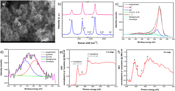
Figure 1. (a) SEM image; (b) Raman spectra; (c), (d) detailed XPS regions of C 1s and N 1s photoelectron lines, respectively; (e), (f) C K-edge and N K-edge NEXAFS spectra, respectively, taken from NG_PD sample.
Download figure:
Standard image High-resolution imageThe most prominent for graphene-like materials 2D peak is often used to estimate the number of graphene layers: full width at half maximum of 2D peak is ∼(48–50 cm−1) suggesting that these structures are predominantly composed of several-layers [S3, S4]. The D peak and the small shoulder of the G peak (D') are typically activated by defects, presence of sp3 carbon, and/or edge effects, but also by doping effects. The intensity of D and D' peaks depend on the type of defects and their concentration in the graphene layer and the size of graphene flakes their folding. The presence of nitrogen atoms in the sample represents structural defects in graphene lattice, contributing to the D band intensity. The variation of the peak intensities of the two types of spectra  imply that the sample is inhomogeneous, which is expected since the post-doping of graphene leads predominantly to surface doping. Contrary to the direct plasma N-graphene synthesis, here the post-plasma doping modifications are localized at the sample surface.
The XPS survey spectrum, taken in the binding energy range 0–600 eV, revealed presence of dominantly carbon, but also oxygen and nitrogen. The elemental composition, obtained from the intensities of the major photoelectron lines after removing the background of Shirley type, was estimated as follows: 96.9 at % of C, 1.54 ± 0.1 at % of N and 1.56 ± 0.1 at % of O. The most intense contribution at 284.4 eV readily attributed to the sp2 C–C bond and accompanied by its shake-up π – π* satellite, figure 1(c), is an evidence of the graphene nature of the material. The contribution at 285.2 eV can be due to the sp3 carbon i.e., defects, while the contribution at 286.3 eV is related to the C–O–C and/or N bonds with sp2 hybridized carbon [25, 26]. The N 1s photoionization, figure 1(d), was fitted to two contributions of equal intensity at 398.8 eV and 400.2 eV, attributed to pyridinic and pyrrolic nitrogen groups, respectively [26, 27].
Additionally, the NEXAFS spectra, presented in figures 1(e), (f), were obtained on the C K-edge and N K-edge. The characteristics sharp C 1s → π* resonance (A) at ∼285.3 eV [28, 29] and the σ* resonance (C) at ∼291.8 eV [28, 30] are detected. The moderate feature detected in between (B) gives indication that small amounts of N and O are present, which is verified also in the peak detected in N K-edge spectrum, figure 1(f). A narrow peak (A) at ∼399 eV is assigned to pyridine-like bonding that arises from transitions from the K-shell to the unoccupied π* orbital [31], while (B) at ∼400 eV is usually assigned to pyrrole/amino groups/substitutional graphite-like bonding . Other contributions (C, D) at ∼402–410 eV, are attributed to N–C/N–H bonding [32].
2.3. Electrical conductivity experiment
The study of the dc electrical resistivity/conductivity of the graphene sheets was conducted on pellets formed with diameter of 8 mm and thickness between 1 and 2 mm. For this purpose about 0.1 g of the graphene/N-graphene sheets was compacted in a hydraulic press. Van der Pauw method was used for measuring the electrical conductivity. The needed four contact geometry is achieved by situating four point contacts on the pellet's periphery. This configuration of the contacts ensures that the current lines are parallel to the pellet's plane and thus the measured conductivity is longitudinal (in-plane). Additionally, transversal conductivity perpendicular to the pellets plane is measured by applying two contacts scheme on the two planes of the pellet. Measurements were done using HP4140B pA-meter/dc voltage source. Temperature dependent conductivity/resistivity measurements are conducted on samples in the dark placed in an ARS CSW-202AE closed-cycle helium cryostat working in the temperature interval from 300 to 10 K.
3. Results and discussion
The measured longitudinal conductivity (σ||) values are an order of magnitude higher than the transversal (σ⊥) electrical conductivity measured on the compacted PG and N-graphene sheets, table 1. The observed dependence on the current flow geometry implies that the graphene sheets in the pellets have preferential orientation ordering probably induced during the compaction process. The observed electrical conductivity dependence on the current flow geometry is consistent with the predominant orientation of the graphene sheets in the pellets observed by SEM imaging. Actually, SEM imaging of the pellet's cross section (figure 2) shows the compacted primary graphene sheets forming agglomerates, mostly oriented parallel to the pellet's plane, figure 1(a).
Table 1. Room temperature electrical conductivity σ measured in different current flow geometries and Van der Pauw resistivity ρ|| (300 K/10K) of compacted pristine graphene and N-graphene sheets. The N doping content in at% is also shown.
| σ (S.m−1), 300 K | ||||
|---|---|---|---|---|
| Sample | N, at% | σ⊥ | σ|| | ρ|| (Ω.m), 300 K/10K |
| PG | — | 153 | 1180 | 8.5 × 10⁻⁴/1.07 × 10−3 |
| NG | 0.24 | 185 | 1330 | 7.4 × 10⁻⁴/1.01 × 10−3 |
| NG_PD | 1.5 | 216 | 1460 | 7.1 × 10⁻⁴/1.04 × 10−3 |
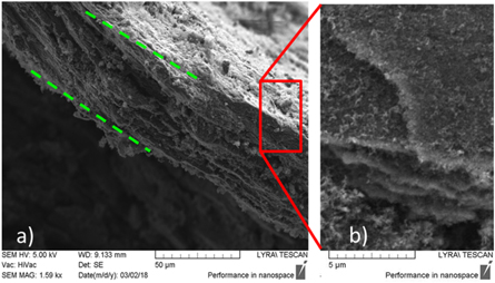
Figure 2. (a) SEM images in cross section of a pellet showing in-plane ordering of N-graphene sheets in platelets (multiple stacked layers) and (b) magnified image taken from the red squared area.
Download figure:
Standard image High-resolution imageТhе treatment of graphene-based free standing sheets is a complicated problem because the sheets are known to react during their processing. The observed near parallel orientation of the sheets can be induced by the compaction process during pellets' formation. As a result a network of connected graphene sheets could be formed. Graphene sheets are known to agglomerate in a composite due to their strong van der Waals attraction. Our observations support a process of self-organization of the graphene sheets according to their orientation with respect to the plane of the specimen. Further, the ordered graphene sheets form electrically percolated paths and the electric response of the composite as a whole is affected by such stacking. This arrangement yields a highly anisotropic conductive system.
The high longitudinal electrical conductivities measured could be due to the excellent properties of the individual graphene sheets. Because of the highly preferred in-plane orientation of the large surface area graphene sheets induced by the compaction process, the measured longitudinal conductivity yields mainly the intrinsic conductivity of primary single sheet for the in-plane direction. From another point of view, the application of pressure during the pallets´ preparation modifies the bulk density and influences the conductivity, as observed earlier [33], by enlarging the contact area between the graphene sheets and leads to increased conductivity. The electrical conductivities of the pellets were studied previously as a function of the bulk density and were found to depend on it. The study suggested bi-linear relationship observed for powder compacts around the percolation threshold [19]. All samples chosen for the present study are of similar density 0.4 ± 0.01 g cm−3 and show electrical conductivity just above the percolation threshold thus ensuring stable current flow.
Further, with the aim to establish the dominant conduction mechanism, temperature dependences of the resistivity ρ(T) are recorded in the temperature interval 10 K < T < 300 K. The current is limited to 10 mA, and measured voltage values are typically about 100–150 mV. The samples are mounted in the cryostat under vacuum conditions and cooled slowly to 10 K at average rate of about 2 K min−1 and at every measurement point the temperature is set constant during the resistivity measurements.
The temperature dependences of resistivity of the samples prepared using the described different N doping procedures are presented in figure 3. Pristine graphene characteristics are also depicted for comparison. Figure 3(b) shows typical linear current-voltage characteristics confirming the Ohmic contact character for current values ranging from 1 to 10 mA. The room temperature conductivity values σ(300 K) reveal explicit influence of the N doping content, the higher at% sample being higher in conductivity (table 1).
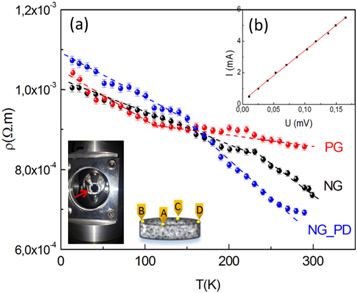
Figure 3. (a) Temperature dependences of the resistivity ρ(T) of compacted graphene and N-graphene sheets. The lines are guides to the eye. (b) Typical current-voltage characteristics. Inset: The mounted sample and schematic for the contacts setup are also shown.
Download figure:
Standard image High-resolution imageFurther, the temperature dependences of the resistivity/conductivity for all samples show thermally activated transport. An increase of resistivity with decreasing temperature  is observed, being opposite to the typically metallic behaviour
  that could be expected for highly conducting media. On the contrary, the
  is characteristic for an insulating state or a localized system [5].
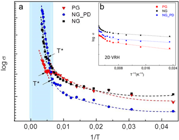
Measured temperature dependences ρ(T) from figure 3 besides showing non-metallic behaviour in the whole temperature range, reveal also change of the slope at a certain temperature T*. As seen from figure 3, no single law can fit the entire curve of the conductivity. Actually, two distinct behaviours at low and high temperatures are distinguished in the thermally excited transport. The characteristic temperature T* indicates a manifested transition between two competing physical processes.
Such anomalous temperature dependent transport in graphene is reported for CVD grown material [34], nano ribbons [35] and rGO [36]. Indeed, it is known that a variety of independent contributions to electron mobility in graphene are possible, depending on carrier density and temperature range, which could influence nontrivially the conductivity. The anomalous temperature dependence of graphene conductivity has been theoretically approached by accounting for the competition of thermal activation, screened impurity scattering, and phonon scattering [5, 37]. It was shown that graphene could exhibit  behavior or the expected 'metallic' behaviour
  depending on carrier density and temperature ranges [4, 5]. Moreover, previous works reported that graphene transport properties are sensitive to the presence of disorder within the graphene matrix, i.e. [34].
Conduction mechanisms are frequently investigated in the presence of disorder in intrinsically conducting media. For metals or nanocrystalline semiconductors, the effects of disorder are manifested as an increase of the low temperature resistivity because of effects of weak-localization and electron-electron interactions. The transport is described by variable range hopping (VRH) mechanism [38]. The compacted graphene sheets under investigation here indeed form such a partially disordered system composed of stacked up together otherwise conducting individuals. Thus, the conductivity could be governed by hopping and tunnelling between separate graphene sheets within the pellet.
It is known that hopping conduction can be in the form of two main mechanisms: nearest neighbour hopping (NNH) and VRH. The two mechanisms usually proceed simultaneously while one of them is dominant depending on the specific experimental conditions. At low temperatures the dominant mechanism is variable range hopping. VRH has been observed in disordered systems, including amorphous carbon and involves consecutive inelastic tunnelling processes between available localized states [39, 40]
The typical expression for VRH conductivity σ considered according to Mott [38] is:

Here, the exponent γ differs for different hopping mechanisms, being  where d denotes the dimensionality, with d = 2 for 2D and 3 for 3D case. Mott-VRH assumes density of states (DOS) near Fermi level N(EF
) constant. An exponent γ of 1/2 corresponds to Efros and Shklovskii (ES) VRH, and 1 for NNH, respectively. Efros and Shklovskii [40] showed that Coulomb interactions between different hopping charged sites result in DOS depletion near the Fermi level and formation of Coulomb gap. The exponent in this case is independent of dimensionality and equals ½.
where d denotes the dimensionality, with d = 2 for 2D and 3 for 3D case. Mott-VRH assumes density of states (DOS) near Fermi level N(EF
) constant. An exponent γ of 1/2 corresponds to Efros and Shklovskii (ES) VRH, and 1 for NNH, respectively. Efros and Shklovskii [40] showed that Coulomb interactions between different hopping charged sites result in DOS depletion near the Fermi level and formation of Coulomb gap. The exponent in this case is independent of dimensionality and equals ½.
Further, the analysis of the temperature dependences of the conductivity from figure 3 in the high temperature range T > T* shows that all curves fit a simple temperature activated form:

where Ea is hopping activation energy. The temperature dependences of the conductivity are depicted in figure 4(a) for all samples showing linear dependence on T−1 in this temperature range (Arrhenius plot) which is consistent with NNH mechanism. The activation energy values Ea (table 2) are of the order of 3 to 10 meV which is consistent with the typical energy scales for NNH thermaly activated transport [41] in graphene films and graphene nanoribbons [35, 42]. Assuming  [38] and the graphene nearest neighbour distance d = 1.42 Å, the localization length of the electronic wave function α values could be deduced.
Figure 4. (a) Temperature dependences of conductivity on a logarithmic scale according to equation 2. The straight lines are fits to simple temperature activated behaviour for T > T* (the shaded area). For temperatures lower than T* the behaviour differs from Arrhenius law. Arrows point at the position of T*; (b) Temperature dependences of conductivity and fits (dashed lines) according to Mott-VRH for T < T*.
Download figure:
Standard image High-resolution image
Table 2. Characteristic parameters of the two conduction mechanisms observed calculated from the fits to the experimental data.
| Sample | Ea × 10 −3 eV | T0 × 10 −4 eV | T* (K) | N(EF) eV −1 cm−2 | Rh, Å | α, Å |
|---|---|---|---|---|---|---|
| PG | 3 ± 0.8 | 0.59 ± 0.02 | 223 | 5.3 × 10¹¹ | 33 | 1.8 |
| NG | 11 ± 0.3 | 0.22 ± 0.05 | 182 | 1.1 × 10¹² | 27 | 7.9 |
| NG_PD | 8 ± 0.4 | 0.37 ± 0.03 | 157 | 1.9 × 10¹² | 24 | 6.7 |
On the contrary, a change to a steeper functional dependence when the temperature is decreased (T < T*) suggests the onset of different temperature activated transport process that is best explained by transport via Mott hopping mechanism. All curves fit behaviour similar to Mott's approach to 2D VRH in disordered systems:

Here T0 is a characteristic coefficient which depends on the 2D DOS N(EF ) as follows:

where  is the Boltzmann constant. Figure 4(b) presents the conductivities versus T−1/3
for the three samples. The linear fits clearly show that the temperature dependence is consistent with the 2D VRH model (γ = 1/3). Satisfactory fits were obtained with correlation coefficients
is the Boltzmann constant. Figure 4(b) presents the conductivities versus T−1/3
for the three samples. The linear fits clearly show that the temperature dependence is consistent with the 2D VRH model (γ = 1/3). Satisfactory fits were obtained with correlation coefficients  From fitting analysis and using equations (1) to (4) values of the characteristic parameters for the two transport regimes, i.e. T0 (being the slope in the high temperature limit), T*, N(EF
), are deduced and listed in table 2. The average hopping distance Rh
between the localized states is estimated at the crossover temperature T* (table 2) using equation 4 and the following expression [38]:
From fitting analysis and using equations (1) to (4) values of the characteristic parameters for the two transport regimes, i.e. T0 (being the slope in the high temperature limit), T*, N(EF
), are deduced and listed in table 2. The average hopping distance Rh
between the localized states is estimated at the crossover temperature T* (table 2) using equation 4 and the following expression [38]:

The N induces in the VRH system an increase in the hopping probability and hopping distance, and decrease in the resistance. It should be noted that the condition  which is required from Mott VHR strongly localized conditions is satisfied at the transition temperature.
In order to check the possibility for Efros-Shklovskii (ES-VRH) mechanism to be valid at low temperatures, the critical temperature Tc under which ES is applicable was determined using the expression [40]:

where ε0 and ε are the vacuum permittivity and the dielectric constant of the material. Assuming ε = 6 [43] the calculated Tc values were found to be lower than 1 K which is out of the temperature range of our measurements. Thus, the Coulomb interaction can be neglected, the used assumption for N(EF ) being constant is applicable and Mott-VRH is concluded as the dominant conductance mechanism at temperatures T < T* here studied. It should be noted that the graphene samples under investigation are composed of compacted graphene sheets in a pellet and the stacks of individual sheets form 3D structure [38, 44]. Obviously, the two-dimensional (2D) character reflected by the observed ∼T−1/3 dependence is consistent with the 2D structure of the sheets. Hopping events might occur between the distinct graphene stacks by consecutive inelastic tunneling processes.
We should point out that the conductivity σ(300 K) of the samples is high because of the highly conductive individual graphene sheets while the insulating temperature behaviour demonstrated is due to the disorder induced during the stacking of the material sheets.
Summarizing our results, the incorporation of N pronouncedly influences the transport mechanism consistent with other observations [45]. The conductivity of the N doped material increases, and accordingly, the estimated density of states show an increase with N-doping compared to the pristine material as the inclusion of N donates an extra electron per added N atom and to the electron conduction paths. The transition point from NNH to Mott-VRH moves to lower temperatures and higher conductivity with increasing N doping. After the transition to VRH is reached the influence of N doping is not much pronounced and the disorder is dominating the localization.
4. Conclusion
In this work the electrical conductivity mechanism of pristine graphene and N-graphene sheets compressed into pellets is reported for the first time. Orientation dependence of the conductivity is due to the preferential orientation of the free standing graphene sheets parallel to the pellets' plain. The synthesised material conductivity displays a highest measured value of (3500 ± 350) S/m, which is comparable or exceeds other reported values for graphene sheet powders obtained by different methods [46, 47]. It could be ascribed to obviously highly conductive primary sheets forming a conductive network with numerous interfaces between them. The observed overall insulating behaviour at temperatures lower than 300 K is disorder induced due to the structural configuration of the graphene sheets agglomerates. The charge transport indicates a transition from thermally activated near–neighbour hoping at relatively higher temperatures to variable range hopping via 2D localization at lower temperatures. The observed charge transport mechanism is typical for partially disordered systems like nanocrystal arrays. This investigation provides insight on the conductance properties of self-standing graphene sheets widely needed for application purposes as an alternative to surface-supported graphene. The investigated material, produced by microwave plasma-based method is of a high quality and fabricated on a large scale in a reproducible manner and at low cost.
Acknowledgments
This work was performed under the framework of the PEGASUS (Plasma Enabled and Graphene Allowed Synthesis of Unique nano-Structures) project, funded by the European Union's Horizon research and innovation program under grant agreement No 766894. Work partially funded by Portuguese FCT - Fundação para a Ciência e a Tecnologia, through EAGER project (PTDC/NAN-MAT/30565/2017) and under projects UIDB/50010/2020 and UIDP/50010/2020. The authors would like to thank S. Russev for the SEM images. M A, E V, K K and Zh K thank the European Regional Development Fund within the Operational Programme 'Science and Education for Smart Growth 2014–2020' under the Project CoE 'National center of mechatronics and clean technologies 'BG05M2OP001-1.001-0008'.
Data availability statement
The data that support the findings of this study are available upon reasonable request from the authors.
Declaration of competing interest
The authors declare that they have no known competing financial interests or personal relationships that could have appeared to influence the work reported in this paper.
CRediT author statement
E V and N B wrote the paper. E V formulated the research idea and analysis of the data. K K performed the conductivity experiments and analysis of the data. N B, A D, E F fabricated of the samples and analysis of the data. M A performed Raman spectroscopy measurements. N B, O M N D T performed XPS measuremants and analysis. T S performed NAXAFS measurements. Zh K, L L A and E T analysis of the data.
Supplementary data (0.1 MB DOCX)