
Abstract
Helium-plasma irradiation induces nanostructure formation on metal surfaces. This study investigated the photocatalytic performance of tungsten (W) oxide nanostructures formed on a thin film and the loading effects of noble metals. Methylene blue (MB) degradation was performed, and the performance of different nanostructured samples formed on thin-film and sheet W with changing the oxidization temperatures was compared; the differences were discussed in terms of the oxidation degree and vacancies. Moreover, noble metals (Pt, Ag, Au) were loaded onto the nanostructured sample oxide by magnetron sputtering as cocatalysts. The MB degradation ability was significantly enhanced by Pt loading. The results showed that nanostructuring and Pt support by using dry processes are novel routes for fabricating highly active photocatalysts.
Export citation and abstract BibTeX RIS

Original content from this work may be used under the terms of the Creative Commons Attribution 4.0 licence. Any further distribution of this work must maintain attribution to the author(s) and the title of the work, journal citation and DOI.
1. Introduction
Two of the key challenges of the twenty-first century are processing increasingly severe environmental pollution and meeting energy demands. Photocatalysis provides a perfect way to solve these two issues at the same time [1–4]. For example, semiconductor photocatalytic degradation of pollutants is an energy-saving, pollution-free, and high-efficiency technology. Various semiconductor metal-oxide photocatalysts have attracted comprehensive attention. For example, research on titanium oxide continues to be an area of both academic and industrial activity. However, using only ultraviolet light (UV) limits its application. Recently, tungsten oxide (WO3) has been regarded as a novel photocatalyst because it can use visible light effectively; this light accounts for nearly half of solar energy. As a visible light-responsive photocatalyst, WO3 has been widely concerned due to its narrow bandgap (2.4–2.8eV) [5, 6] and potential photocatalytic capability.
However, the photocatalytic efficiency of a pure WO3 photocatalyst is still low [7, 8], and many attempts have been made to improve the photocatalytic performance. Surface nanostructuring is one of the mainstream strategies for enhancing photocatalytic activity because the photocatalytic process occurs on the surface. Fiberform nanostructure (FN) formed on a tungsten (W) surface using helium (He) plasma irradiation provides the direction and drive for the photocatalyst application due to the brief formation time, pollution-free process, large surface area, and high optical absorptivity of FN. Additionally, He plasma-induced FN has been identified on the surface of various metals, including molybdenum [9], titanium [10], tantalum, iron [11], rhenium, iridium [12, 13], rhodium, and ruthenium [14]. The FNs of metal oxides, such as W oxides [15–18], iron oxides [19, 20], titanium oxides [21, 22], niobium oxides [23], and vanadium oxides [24], which are created by He plasma irradiation, have been widely applied in the photocatalytic field since the FN was discovered.
WO3 has various nanostructures, included one-dimensional (1D) structures, such as straight and smooth nanorods [25]; uniform wire-like morphology nanowires [26]; rod-like [27] and as-electrospun structure nanofibers [28]; tubular structure nanotubes [29]; two-dimensional (2D) nanosized flake-shaped nanosheets with a flat surface and high aspect ratio [30, 31]; and three-dimensionally (3D) ordered macroporous WO3 materials [32]. The FN sample used in this study was comprised of nanofibers with complex network structures. It was different from 1D and 2D structures and likely close to the 3D nanometric filament structure. The reported 3D structure was also mesoporous, which may have been an advantage to the photocatalytic performance; the structure in this study was comprised of nanofibers, so the porosity could have been higher [33] than reported.
Thin film is recommended over sheet metals because it is low in cost, simple to make, and easy to popularize. Oxidation degree and oxidation vacancies act as a sensitive part of the properties of WO3. Previous research has investigated the effect of either oxidation degree [18] or oxidation vacancies [34–37] on photocatalytic activity, but it has not related oxidation degree and oxidation vacancies to photocatalytic performance or provided direction for designing a highly active photocatalyst.
Besides surface nanostructuring, noble metals (Pt in most cases [38–41]) have been widely used as cocatalysts to improve the photocatalytic activity as they can change the distribution of electrons and can prevent electron-hole recombinations.
This study investigated the photocatalytic activities of a series of nanostructured WO3 samples (sheet and thin-film) and that loaded with noble metals (Pt, Ag, Au). Based on a series of nanostructured WO3 (sheet and thin-film), oxidation degree and oxidation vacancies were systematically compared. Through this investigation, an understanding of the link between oxidation degree and oxidation vacancies and photocatalytic performance was gained. The photocatalytic performance of the materials was measured using methylene blue (MB) degradation.
2. Experimental section
2.1. Photocatalyst preparation
Two types of samples were used in the experiment: sheet (PLANSEE, 0.2-mm thickness, 99.97% purity) and thin film. The samples were 5 × 5 mm2. W thin films were deposited on a silica glass (Labo-USQ, 0.5-mm thickness) using a radio frequency (RF) magnetron sputtering apparatus. Before the deposition, the glass was cleaned using deionized water and ethanol and then was air-dried [42]. Helium plasma irradiations were conducted in the linear plasma device NAGDIS-II, whose setting details can be found elsewhere [14]. After irradiation, the nanostructured W samples (sheet and thin-film) were calcined at different temperatures in air for 30 min using an electric furnace (FO100). A layer of noble metals (Ag, Au, and Pt) was deposited using an RF magnetron sputtering apparatus. The layer thickness of noble metals was characterized as the product of sputtering time multiplied by the deposition rate on the flat plane. Since the noble metal depositions were performed after the nanostructure formation, the actual thickness of the noble metal layer on the nanostructures was different from the measured thickness. The thickness was used as an index of the amount of loading.
2.2. Photocatalytic experiments
The photocatalytic performances of the samples were measured using MB degradation experiments under visible light. A high-pressure Xenon lamp with a blue additive color dichroic filter and a cut-off filter permitting >400 nm was used to provide visible light in a wavelength range of 400–500 nm. The MB absorption in the wavelength range of 400–500 nm was not significant, as shown in figure 1.

Figure 1. The absorption spectra of methylene blue solution.
Download figure:
Standard image High-resolution imageMB is often used as a substrate in photocatalytic degradation. An issue when using MB to check photocatalytic performance under visible light has been reported due to its light absorption [43]. However, Komori et al confirmed that MB decomposition occurred using K-edge XANES and showed that partially oxidized nanostructured W is an excellent photocatalyst for decolorizing MB under near-infrared light (λ > 800 nm) [17, 18]. Thus, MB can be used to assess the photocatalytic activity at least under the conditions used in this study. The photocatalytic activity of the materials can be defined from the MB decomposition rate (i.e., the rate of MB concentration change). The concentration of MB was deduced through converting the absorbance, which was recorded using a UV–vis spectrometer (UV-2600). Concerning the relationship between the microstructure of the photocatalysts and their performance, the influence of the surface morphology on the photocatalytic activity was investigated using MB [42]. The formation of FN on the W sheet surface was found to increase MB decolorization three times more than on the pristine WO3 sheet sample.
2.3. Characterization of materials
All W thin-film samples were synthesized on silica glass using RF magnetron sputtering with argon gas at room temperature. The chamber was evacuated to ∼10−4 Pa before deposition. A 100-mm diameter and 1.0-mm thick W disc (99.95% purity) was used as a sputtering target. The RF power and working pressure were 100 W and 1 Pa, respectively. After irradiation and calcination, the surface composition analysis of the nanostructured W oxide samples (sheet) was accomplished using x-ray photoelectron spectroscopy (XPS; Shimadzu ESCA-3300) using Mg Kα (1253.6 eV) as the x-ray source. XPS measurements of the nanostructured W thin-film oxide samples were performed using a different device (ESCALAB 250Xi) with Al Kα emission for the x-ray source. Transmission electron microscope (TEM) images and energy dispersive x-ray spectroscopy (EDS) analysis of the samples was acquired from the JEOL JEM-2800 TEM.
3. Characterization
3.1. Nanostructured W thin film
A previous study found that a uniform nanostructured layer was formed on the surface of 300-nm-thick W thin films (WNTF), while non-uniform isolated nanostructures were formed when the film thickness was 100 nm or less [42]. This raised the question of whether WNTF and W sheet irradiated with the He plasma (WNano) have similar degradation ability at the same calcination temperature; verifing whether WNTF can achieve a similar oxidation state to WNano after oxidation is important. Figure 2(a) shows the XPS (ESCALAB 250Xi) spectra of WNTF subjected to calcination at 523K compared with WNano calcined at 523 K (figure 2(b)). Only the W6+ species peak was found, which demonstrated that the coexistence of W0 and W6+ species, which is thought to be one of the key factors of photocatalytic performance [17], was not been found on the surface. Temperature dependences of the ratios of W to the sum of W trioxide and W (W/[WO3+W] = the sum of the peak area of  and
and  ))/the sum of the peak area of
  ,
,  ,
,  , and
, and  ) on the sheet and thin-film samples are plotted in figure 3. The ratio of W decreased both on WNTF and WNano as the calcination temperature increased. As shown in figure 3, the calcination temperature difference in an analogous oxidation state was 50 K. In other words, the necessary oxidization temperature was lower for the thin-film sample than the sheet samples.

Figure 2. W4f XPS spectra of (a) WNTF and (b) WNano under calcination at 523 K for 30 min.
Download figure:
Standard image High-resolution image
Figure 3. The ratio of tungsten to the sum of tungsten trioxide and tungsten (W/[W+WO3]) on the surface of the 300-nm-thick thin-film and sheet samples at various calcination temperatures.
Download figure:
Standard image High-resolution imageThe formation of oxygen vacancies is thought to enhance charge separation and greatly improve photocatalytic activity [34–36]. Measuring the chemical state of oxygen by XPS is one of the principal means for obtaining detailed information about oxygen vacancies. In this study, a comparative analysis of the oxygen vacancies was performed between WNano and WNTF using XPS at various calcination temperatures, and the characteristics of high photocatalytic performance samples were proposed. Figure 4 displays the O1s spectra of WNTF at 373K. The O1s spectra were fitted with two peaks at 530.5 eV and 532 eV [37], which originated from lattice oxygen (OL) and oxygen vacancies (OV), respectively.

Figure 4. O1s XPS spectra of WNTF under calcination at 373 K for 30 min.
Download figure:
Standard image High-resolution imageFigure 5 summarizes the proportion of oxygen vacancies (OV) to the sum of oxygen lattice (OL) and oxygen vacancies (OV) as a function of the calcination temperatures for WNano and WNTF. The ratio of oxygen vacancies (OV) to the sum of oxygen lattice (OL) and oxygen vacancies (OV) was equal to the ratio of the peak area of OV to the sum of the peak area of OV and OL. The ratio of OV decreased with increasing temperatures, especially for WNTF.

Figure 5. The ratio of OV to the sum of OV and OL (OV/[OL+OV]) on the surface of 300-nm-thick thin-film and sheet samples at various calcination temperatures.
Download figure:
Standard image High-resolution image3.2. Loading effect
XPS is also a convenient quantitative spectroscopic technique for measuring the elemental composition of a surface. The atomic ratios of X/(X+W) were achieved using the peak areas and sensitive factors of Ag(3d), Au(4f), Pt(4f) and W(4f). Table 1 shows the variation of the surface coverage of noble metals (Ag, Au, and Pt) on nanostructured WO3 with different deposition thicknesses. As described in section 2, the deposition thickness was derived from the deposition rate measured on a flat sample and was used as an index for the amount of deposition. As seen in table 1, the surface coverage did not differ as much as deposition thickness among the Pt/WO3 samples.
Table 1. The fraction of noble metals (Ag, Au, and Pt) on the nanostructured WO3 at different deposition thicknesses.
| X | Deposition thickness [nm] | [X\(X+W)] [atomic%] |
|---|---|---|
| Pt | 5 | 89.90 |
| Pt | 10 | 94.11 |
| Pt | 15 | 95.58 |
| Ag | 10 | 91.29 |
| Au | 10 | 99.41 |
Figures 6(a)–(b) exhibits high-resolution cross-sectional TEM (JEOL JEM-2800) images of 10-nm-thick Pt supported on a nanostructured WO3 sample (Pt10/WNano[523]). Noble metal layers formed by magnetron sputtering devices are comprised of island structures with ∼8 nm in diameter, and the formation mechanism can be explained by the Volmer-Weber-type growth mode [44–46]. Island structures grow and coalesce as the noble metal film thickness increases. As shown by the TEM analyses (figure 6(b)), Pt nanoparticles formed island structures in this study as well. Although only one sample was observed, the particle size likely depended on deposition thickness, as suggested in previous studies [44–46]. EDS mapping was applied to obtain the distribution pattern of the elements. Figures 6(c)–(f) shows that W fiber was oxidized and Pt was successfully deposited. Based on the preceding analysis (figure 3), it can be speculated that Pt was loaded onto the surface in the mixed state of W and O.

Figure 6. (a)–(c) TEM images of the Pt-loaded WNano sample, and (d)–(f) elemental maps of O, Pt, and W, respectively, using EDX mapping at the area shown in the (c) TEM image.
Download figure:
Standard image High-resolution image4. Photocatalytic experiments
4.1. Comparison between thin-film and sheet samples
Figure 7 shows the MB decomposition rate for 2 hours under visible light irradiation per unit of irradiation area using the following samples: WNTF calcined at (i) 373 K (WNTF[373]), (ii) 423 K (WNTF[423]), (iii) 473 K (WNTF[473]), and (iv) 523 K (WNTF[523]), and WNano samples calcined at (v) 473 K (WNano[473]), (vi) 523 K (WNano[523]), and (vii) 573 K (WNano[573]). It is noted in figure 7 that the irradiation surface area of the WNTF samples (∼4 × 4 mm2) was ∼35% less than that of the WNano samples (5 × 5 mm2). As shown in figure 7, the optimum calcination temperature for WNTF samples was 423 K, while WNano samples had a higher optimum temperature of 523 K. As has been discussed previously [18], one of the factors that manifested the photocatalytic performance was the coexistence of W and W oxides. Full oxidization did not occur on either the  or the
  samples. However, the decreased photocatalytic performance of WNTF samples calcined from 423-473 K could not be explained only by the oxidization fraction.

Figure 7. The decomposition rate of MB under 2 hours of visible light irradiation per unit of irradiation area for WNTF calcined at 373 K, 423 K, 473 K, and 523 K and WNano calcined at 473 K, 523 K, and 573 K.
Download figure:
Standard image High-resolution imageThe oxidation state of WNTF(473) and WNano (523) were quite similar (figure 3). However, the photocatalytic performance of WNTF(473) was not the greatest. Oxidation degree and oxidation vacancies are a sensitive part of WO3 properties. As seen in figures 3 and 5, some differences were found in the oxidation degree and oxidation vacancies of WNano and WNTF. This was due to the synergy between oxidation degree and oxidation vacancies. The ratio of OV/OL on WNTF decreased significantly from 423 to 473 K. Thus, the highest photocatalytic activity was attributed to the W/ WO3 interface and appropriate oxygen vacancies. The different photocatalytic performances were obtained by different thicknesses [47, 48]. For example, the values of steady-state photocurrents under fixed illumination intensity depended on the film thickness of WO3 films [47]. Additionally, WO3 film with a thickness of 2μm showed the highest photocatalytic activity to degrade acid orange 7 under UV illumination [48]. The optimum thickness likely depends on fabrication methods and focused reactions. Because a layer with a thickness of 300nm is sufficient to form a uniform nanostructure [42], the effect of oxidation temperatures and the reason for the differences found in the sheet and thin-film samples were the focus of this study.
4.2. Effect of noble metal support
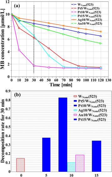
Figure 8(a) demonstrates the time evolution of MB concentrations using (i) WNano(523), (ii) 5-nm-thick Pt-supported WNano(523) (Pt5/WNano[523]), (iii) 10-nm-thick Pt-supported WNano(523) (Pt10/WNano[523]), (iv) 10-nm-thick Ag-supported WNano(523) (Ag10/WNano[523]), (v) 10-nm-thick Au-supported WNano(523) (Au10/WNano[523]), and (vi) 15-nm-thick Pt-supported WNano(523) (Pt15/WNano[523]) as photocatalysts. The activity of the Pt-loaded samples was higher than that of the other samples; the deposition of Pt on WNano(523) had a positive effect on photocatalytic activities. Additionally, the greatest photocatalytic activity was identified with 10-nm-thick Pt loading. The lower photocatalytic activity of Pt5/WNano(523) compared to Pt10/WNano(523) was the result of the shortfall of the Pt deposit. The lower photocatalytic performance of Pt15/WNano(523) was because the layer was so thick that surface activity sites were obscured.
Figure 8. (a) Concentration changes of MB over time in the presence of different samples, and (b) the decomposition rate of MB under 0.5 hours visible light irradiation for different samples.
Download figure:
Standard image High-resolution image
As shown in figure 8, the deposition of Pt and Au on WNano(523) had an active effect on photocatalytic activities, while the effect of Ag support was negative. Young et al [39] found analogous experimental results. The interpretation was based on the formation of the Schottky barrier [49] as an effective photo-induced electron trap that prevented the recombination of electron holes and prolonged electron life. Thus, the effect of noble metals (Ag, Au, and Pt) loading is attributed to the Schottky barrier. In other words, separation of photo-induced electrons and holes becomes easier with a higher Schottky barrier.
The enhancement of photocatalytic performance in ascending order was as follows: 10 nm Ag/WO3, unsupported WO3, 10 nm Au/WO3, and 10 nm Pt/WO3. The bandgap of WO3 was about 2.4-2.8 eV, and the electron affinity was about  eV [50]. The work function of metals [38] and the barrier heights of metals/semiconductors are shown in table 2. The barrier height was derived from the difference between the work function of the deposited metals and the electron affinity of WO3 (
 eV). The photocatalytic activity was found to be higher when the barrier height was greater.
Table 2. The work function of deposits (noble metals) and barrier heights between metals and semiconductors.
| Deposit | Work function (eV) | Barrier height (eV) |
|---|---|---|
| Ag | 4.74 | 1.41 |
| Au | 5.31 | 1.98 |
| Pt | 5.93 | 2.60 |
Surface plasmonic resonance (SPR) [51] is thought to be another interpretation of the enhancement of noble metal loading on semiconductors. However, this is still a controversy, as the flow of the electron is different based on the Schottky barrier (from the semiconductor to the metal) and the SPR effect [52].
5. Conclusion
This study investigated nanostructured W thin film samples (WNTF) fabricated by helium plasma irradiation and used to degrade MB at various calcination temperatures. Comparison of the degradation per unit of irradiation area showed that WNTF calcined at 423 K had comparable performance when degrading MB to nanostructured W sheet samples (WNano) calcined at 523 K. XPS analysis revealed that the optimum calcination temperature is determined by the W/WO3 interface and the concentration of oxygen vacancies. Additionally, among a series of nanostructured WO3 with noble metals (Pt, Ag, Au), 10 nm Pt/WO3 displayed the greatest photocatalytic performance. The deposition of Pt enhanced the decomposition rate by a factor of five, while the Ag deposition had a negative effect on photocatalytic activity. The formation of the Schottky barrier under the junction between the metal and semiconductor likely prevented the recombination of formed electron and hole pairs.
The manufacturing of photocatalysts can be done through two process: the wet process and dry process. Although the wet process is relatively straightforward, its long manufacturing period and remaining liquid waste are key issues. The dry process addresses both these issues. In this study, the nanostructuring and deposition were both conducted using the dry process with plasmas. The results suggested that dry processes can be novel routes for fabricating highly active photocatalysts. Future studies will investigate the photocatalytic performance of reactions other than MB to explore the potential of this process.
Acknowledgments
The authors thank Dr. Tanaka for useful discussion. This work was supported in part by a Grant-in-Aid for Scientific Research 19H01874, Fund for the Promotion of Joint International Research 17KK0132 from the Japan Society for the Promotion of Science (JSPS), and JSPS Bilateral Joint Research Project.