
Abstract
Flexible strain sensors are essential for providing electronic skin with the ability to detect motions and pressure, enabling their use in health applications and robotics. In this context, strain sensors should simultaneously guarantee a high sensitivity and flexibility, with a fast response when applied to the detection of various human motions. Here, we demonstrate a flexible strain sensor made of graphene nanoplatelets encapsulated between two elastomer films with a high sensitivity and stretchability. The liquid-exfoliated graphene nanoplatelets were spray-coated on the first elastomer film and then encapsulated by the second elastomer film. The encapsulated graphene sensor exhibited a high gauge factor, fast responsivity, and high durability. It proved stretchable up to 290% and highly bendable (operating at almost zero bending radius). As an additional key feature, proximity sensing to detect remote motions of a distant object was demonstrated, owing to the unique characteristic of graphene, i.e., variations in its electrostatic in response to the interaction between the surface charges of the elastomer and the electrostatic charges of the remote object. Our work introduces a novel route for the fabrication of flexible graphene sensors with proximity-sensing capability, which are useful for wearable smart devices and human motion detection.
Export citation and abstract BibTeX RIS

Original content from this work may be used under the terms of the Creative Commons Attribution 4.0 licence. Any further distribution of this work must maintain attribution to the author(s) and the title of the work, journal citation and DOI.
1. Introduction
Wearable electronics is an innovative field of technology that is attracting enormous research interest, driven by ever-increasing consumer demand. Wearable devices find application not only in consumer electronics but also in the context of human motion detection, body activity tracking, and health monitoring [1, 2]. In such devices, the strain sensor is a crucial component that allows mechanical deformation to be transduced into electrical signals. Wearable and skin-mountable sensors need to comply with stringent requirements with regard to flexibility, robustness, stretchability, lightness, and biocompatibility. For these reasons, various flexible strain/pressure sensors have been recently developed using metal nanoparticles [3, 4], nanowires [5–7], and low-dimensional carbon materials [8, 9].
Graphene is one of the most promising candidates for both flexible electronics and wearable sensors due to its excellent electrical and mechanical properties [10–13]. Graphene grown by chemical vapor deposition (CVD) has been used as an electrical channel in strain sensors with high sensitivity, but such devices showed small stretchability and entailed a complex and expensive fabrication process [14, 15]. Instead, other researchers proposed strain sensors based on composites of graphene mixed with rubber-like materials [16–20]. Despite their high flexibility, these graphene-based composite sensors have shown limits in sensitivity due to the large number of electrical paths required for percolation [21]. In this framework, it is necessary to develop an alternative approach to fully exploit the superior properties of graphene and create strain sensors with a high sensitivity and stretchability at low cost.
In this paper, we propose a simple, efficient, and inexpensive strain sensor based on graphene. The sensors are fabricated by sandwiching uniformly spray-coated graphene nanoplatelets (GNPs, commercially available at low price) between two polydimethylsiloxane (PDMS, the most common silicon-based organic polymer) films. The fabricated graphene-based sensors are highly sensitive, flexible, stretchable, and lightweight. Owing to these properties, the sensor can be applied to detect strain and a variety of motions, ranging from small vibrations to pressing, bending, and large stretching. In addition, the sensor responds to proximity effect: thus, Remote motions (e.g., of a finger or a stylus) can be detected via changes in the electrostatic doping of graphene. Overall, the GNP-PDMS sensor shows a high sensitivity, fast responsivity, and high durability, in combination with flexibility and low cost. A graphene-based sensor with such characteristics holds a great promise for future applications in consumer electronics, motion sensing, and robotics
2. Results and discussion
2.1. Fabrication and characterization of the GNP-PDMS sensors
The fabrication process of the elastomer-encapsulated graphene sensors is depicted in figure 1. The sensor consists of sprayed GNPs nanoplatelets encapsulated by 90-μm-thick PDMS films. Raman spectroscopy was used to evaluate the structural properties of the GNPs sprayed on the PDMS substrate. As shown in figure 2(a), the Raman peaks of graphene and PDMS [22] were clearly identified. The strong D peak is attributed to various defects in the graphene lattice, especially edge defects typical of micro-sized GNPs. The small 2D to G intensity ratio (I2D/IG = 0.3), along with its large full width half maximum (FWHM) of 2D (FWHM = 95 cm-1) indicate that the GNP are on average composed of five or more graphene layers. [23, 24]. Thickness and lateral size of GNPs are confirmed by atomic force microscopy (AFM) in figure 2(b). The measured thickness (figure 2(c)) and lateral size (figure 2(d)) range between 7–12 nm and 0.24–1.33 μm2, respectively. The Raman spectra of the GNPs do not change after the spray-coating on PDMS, indicating that the sensor fabrication process do not alter the GNPs' properties (figure S1(a) is available online at stacks.iop.org/MRX/7/045603/mmedia). After the spray-coating onto PDMS, the GNPs appear homogeneously distributed, forming a uniform, atomically thin film of interconnected nanoplatelets (figures 2(e) and S1(b)).

Figure 1. Fabrication process for the GNP-PDMS sensors.
Download figure:
Standard image High-resolution image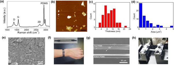
Figure 2. (a) Raman spectrum of GNPs deposited on a PDMS substrate. (b) AFM image of the exfoliated GNPs sprayed on SiO2; (scale bar is 2 μm) (c) Lateral size and (d) thickness distributions of the GNPs measured by AFM (e) SEM image of GNPs covering the PDMS before encapsulation. (f) Image of a GNP-PDMS sensor worn as a wristband. (g) Cross-section SEM image of the GNP-PDMS sensor. The GNPs sandwiched by the PDMS films are uniformly stacked. (h) Image of our custom-made stretch-testing instrument.
Download figure:
Standard image High-resolution imageThe fabricated graphene-PDMS (GNP-PDMS) sensor is shown in figure 2(f). The sensor is light and flexible; thus, it is easy to wear on a wrist, while performing daily (or sport-related) activities. The cross-section SEM image in figure 2(g) shows the sprayed GNP layer sandwiched between the two PDMS films. The GNP film forms a continuous layer with a uniform thickness between the two PDMS films. The sensor thickness is 181 μm, with each PDMS film of a thickness of 90 μm and the GNP film of a thickness of 1.1 μm. The GNP distribution and the shape of GNPs/PDMS film are maintained and there is no any recognizable change of interface between GNPs and PDMS after stretching tests (figure S2).
2.2. Change of electro-Mechanical properties of G-PDMS sensors applied mechanical stress
The electromechanical properties of the sensors were tested with the custom-made instrument shown in figure 2(h). The sensor response to increasing applied strain (ε) values (ε = 5%, 10%, 20%, 30%, 40%, and 50%) is reported in figure 3. The increasing strain values were applied at a rate of 1 mm/s, followed by a release step (cycles of stretching/releasing, figure 3(a)). When each strain was released, the sensor fully recovered the initial resistance (R0). Figure 3(b) plots the relative change of resistance (∆R) versus strain (ε): The graph shows an exponential increase, with ∆R/R0 reaching 0.78 at ε = 50%. The experimental ∆R/R0 data can be fitted with remarkable agreement. The fitted curve follows the equations:  (coefficient of determination = 0.9997). We investigated the effect of the GNP thickness on the sensor performance, as shown in figure S3(a). ∆R/R0 is observed to scale with the GNP concentration (and hence with the GNP film thickness), and figure S3(a) shows that ∆R/R0 decreases with the increase of the film thickness. The gauge factor is used to classify the sensitivity of strain sensors and, in resistive-type sensors, is defined as GF = ∆R/R0ε (i.e., the ratio of the relative change in electrical resistance versus the applied strain, where R, R0, and ε are the resistance of the strained sensor, the unstrained resistance, and the applied strain, respectively). Our GNP-PDMS sensor (fabricated with 0.35 mg ml−1 GNP) has GF = 1.55 for ε = 50%. To evaluate the durability of the sensor, it was tested with continuous cycles of stretching (∆ε = 50%) and releasing at a rate of 0.5 Hz (figure 3(c)). The sensitivity of sensor decreased at early cycles, but ∆R/R0 was stabilized over cycles and was maintained over 0.5 during 2,500 cycles, indicating that the GNP-PDMS sensor is reliable and highly durable. In figure S4, drift behaviour at initial cycles is due to thermal drift of carbon-tape contacts and to the stabilization of the GNP-PDMS interface. When applying voltage to the GNP-PDMS, the current initially increased rapidly and then stabilized over time (figure S5). We think that the drift behaviour of our sensor can be improved by implementing more suitable contacts. Figure S3(b) shows the stretchability of GNP-PDMS sensors fabricated with 0.25 and 0.35 mg ml−1 GNPs. The GNP-PDMS sensor fabricated with 0.25 mg ml−1 GNPs stopped working at 80% strain, as the PDMS becomes fractured. On the other hand, the GNP-PDMS sensor fabricated with 0.35 mg ml−1 GNPs is still conductive over 80% strain, and the fracture of the sensor occurs in the PDMS structure at 100% strain (the fracture is not related to the GNP layer). The maximum stretchability can be further increased by modifying the PDMS thickness. Figure S3(c) shows the stretchability of a 100-μm-thick GNP-PDMS sensor. The sensor is still conductive for ε > 200% and is observed to fracture for ε > 290%.

Figure 3. Electromechanical response of the GNP-PDMS sensor to strain. (a) Stretching/releasing test with increasing strain values (∆ε = 5/10/20/30/40/50%). The stretching/releasing speed was set to 1 mm s−1; the current was measured at bias voltage of 1 V during the stretching phase. (b) Relative change of resistance versus strain graph (R0 is the initial resistance; bias voltage = 1 V). (c) Durability of GNP -PDMS sensor: stretching/releasing cycles (50% strain) at a 0.5-Hz rate.
Download figure:
Standard image High-resolution imageThe electromechanical properties of the GNP-PDMS sensor can be discussed with reference to those of strain sensors built with other graphene-based materials. Strain sensors made with CVD graphene generally have low stretchability because CVD graphene can endure strain up to only ∼20% before fracture [25]. Therefore, CVD graphene appears unsuitable to design highly stretchable sensors, which should ideally benefit from the elastic properties of graphene. In contrast, sensors based on graphene-polymer composites significantly outperform those based on CVD graphene, with far higher stretchability [21, 26]. The graphene nanoplatelets embedded in the composite should be well-distributed to satisfy the percolation mechanism needed for efficient charge hopping, which is required for increasing the sensitivity and detecting small strains. In previously reported sensors based on graphene–polymer composites, the graphene nanoplatelets had to either remain in physical contact during operation to remain on an electrical path or be dispersed in the polymer at a high enough concentration (above the percolation threshold) to let electrons flow by hopping [21]. When such graphene–polymer sensors are stretched, the distance between graphene nanoplatelets increases, reducing the density of electrical paths, which leads to an increase of the resistance. In contrast, our GNP-PDMS sensor has vertically stacked graphene films in the two-dimensional interface of the PDMS. Therefore, when it is stretched, the resistance increases owing to the reduction of the overlapped area between graphene nanoplatelets.
To investigate the response time, a 50% strain was periodically applied by stretching the sensor at fixed frequencies ranging from 0.1 to 1 Hz. As shown in figure 4(a), periodic resistance changes with no significant lagging were observed even at a high frequency of 1 Hz. Drift behaviour was observed in the fabricated sensors. But, as shown in figure 3c, the drift behaviour is removed after the stabilization of the GNP-PDMS sensor. Notably, the sensor conductivity remained almost unchanged after stretching, indicating that the GNP network sandwiched between PDMS is highly stable and robust and that the conductance recovery is fast and consistent even at a high frequency.
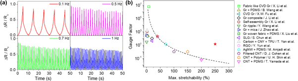
Figure 4. (a) Responsivity of the GNP-PDMS sensor measured at different frequencies of stretching/releasing cycles under Δε = 50%. (b) Summary of the gauge factors and maximum stretchability of the flexible strain sensors. The dashed line indicates the correlation between the gauge factor and the maximum stretchability, which exhibits a tradeoff relationship [5, 14, 26–38].
Download figure:
Standard image High-resolution imageFigure 4(b) summarizes the gauge factors and maximum stretchabilities of previously reported flexible strain sensors [5, 14, 26–39]. As indicated by the dashed line, the gauge factor and stretchability have a trade-off. In general, strain sensors consisting of CVD graphene have large gauge factors over 100, while their maximum stretchability is as small as 5–8 because CVD graphene is mechanically weak due to numerous defects and damage induced during transfer stage [25]. When one-dimensional nanomaterials, such as carbon nanotubes (CNTs) and metal nanowires (NWs), were used for strain sensors, the stretchability could be enhanced by up to 70%–200% at the expense of the gauge factor. However, the GNP-PDMS sensor fully coated by graphene showed an even higher stretchability of 250% and a relatively high gauge factor of 14. As described in the Experimental section, an additional sensor configuration made by patterning the sprayed GNPs with a shadow mask (forming a grid) was also fabricated. The gauge factor of the grid pattern sensor was increased to 313, by two orders of magnitude. However, the maximum strain applicable to the grid pattern sensor was decreased to 41.8% (figure S6(a)). The increased gauge factor and decreased stretchability are related to the number of electrical paths, as mentioned previously. Even though the fully coated sensor has small sensitivity in the range of small strain (figures S3(b) and S3(c)), the grid-pattern sensor has higher sensitivity in the same strain range because of the reduced number of electrical paths, i.e., overlapped GNPs (figure S6(b)). This result shows that it is possible to control the sensitivity and stretchability of the GNP-PDMS sensors by adopting specific patterns. Therefore, the fully coated GNP-PDMS sensor can be used as a highly sensitive sensor in the large-strain regime, while grid-pattern sensor can be applied in the small-strain regime.
A wearable sensor should be flexible and ideally able to operate under extreme torsion/bending conditions. To examine the limit for bending, the GNP-PDMS sensor was bent with different radii, as shown in figure 5(a). The sensor conductivity was maintained not only at a 1-mm bending radius but even when the sensor was completely folded (zero bending radius). This demonstrates the robustness and versatility of our GNP-PDMS sensor, which could be used in 'rugged' conditions, as is often the case for wearable and sports electronics.

Figure 5. (a) Foldability of the GNP-PDMS sensor measured at different bending radii. The resistance increases with the decrease of the bending radius. Note that the completely folded sensor is still operating. ∆R/R0 of the GNP-PDMS sensor for (b) bending motions, (c) pressing motions, and (d) swallowing motions. The sensor attached to a finger sensitively detected the bending of the finger. Slight pressing onto the GNP-PDMS sensor and the motion of Adam's apple were also detected.
Download figure:
Standard image High-resolution imageTo measure actual motions of the human body, the G-PDMS sensor was attached to human skin, as shown in figures 5(b)–(d). The bending motion of a finger was clearly detected by the measured current, as shown in figure 5(b). The level of ∆R/R0 depends on the extent of bending. It is expected that different bending motions of a finger, which cause distinct bending radii and stretched distances, can be detected using the GNP-PDMS sensor. We performed pressure tests with a sensor worn on a wrist (as a watch), as shown in figure 5(c). When a slight pressure was applied with a finger, a distinctive drop in current was registered as a result of the local change in the percolation path of the GNPs. In figure 5(d), we attached the sensor on the midline of the neck and repeated swallowing motion. There are double peaks per one swallow, which is similar to electrical signal change induced by the motion of hyoid bone [39]. When the GNP-PDMS sensor was suspended, it could also detect the small vibration caused by a nearby motor or airflow (figures S7(a) and S7(b)).
In addition, the GNP-PDMS sensor is waterproof, as the graphene was encapsulated by impermeable PDMS films (figure S8). This is advantageous because previously reported polymer-based sensors or skin-like sensors might be useless in water or on rainy days owing to water penetration. Therefore, the GNP-PDMS sensor is useful for sensing various motions of the human body and dynamic stimuli of remote vibration.
The GNP-PDMS strain sensor demonstrated high sensitivity, fast response, and durability, all of which are required for successfully detecting a wide range of human motions. Additionally, our sensor has been designed to detect pressure and proximity when worn on human limbs. This is ideally suited for finger-controlled technological devices (such as smartphones and touch screens).
2.3. Proximity effect of the GNP-PDMS sensors
An additional novelty of our strain sensor is the proximity-sensing function. In contrast to the usual tactile sensors that only detect physical touch, our sensor can detect the non-contact motion of nearby objects as well as touch. As displayed in figure 6(a), the ∆R/R0 of the sensor oscillates in response to the vertical displacement of a stylus pen made of plastic (periodically moving toward and moving away from the sensor plane). The ∆R/R0 peak value is ∼0.25 and corresponds to the smallest distance between the plastic and the sensor. As illustrated in figure 6(b), the operating principle of the proximity sensor can be explained by the electrostatic induction between materials. When two materials with dissimilar contact electrification are in contact or spaced in the proximity range, the mobile charges on the facing sides of the two materials are spontaneously redistributed to screen the generated electric field. Due to the partial electric-field screening of PDMS with the external materials, the contribution of graphene electrons to the electric field screening is relieved, driving excess electron movement that induces the resistance change of the sensor. Given that the PDMS and the other material can be modeled as a parallel-plate capacitor, it is very likely that ∆R/R0 becomes more sensitive with the reduction of the relative displacement. Furthermore, thinner PDMS causes a larger impact of the graphene layer on the current flow. Additionally, ∆R/R0 is observed to increase when the plastic is rubbed to generate static charges, as shown in figure 6(a). The charge of the rubbed plastic is enhanced when the plastic is rubbed with a dissimilar electrostatic material. Figure S9(a) shows the ∆R/R0 response to the motion between a human finger and the sensor. The current change caused by finger movement toward the sensor is shown in the Supplementary video. We changed the proximity test condition from cycles of moving toward-moving away to cycles of moving toward-stop-moving away to find out if moving direction can be detectable from resistance change. (figure S9(b)) When the finger moves toward the sensor, ∆R/R0 is increased to positive value, whereas as soon as the finger stops, ∆R/R0 returns to zero. When the finger moved away from the sensor, ∆R/R0 decreases to negative value, then returns to zero when the finger stops. This indicates that the GNP-PDMS sensor can detect moving direction in the remote sensing mode.

Figure 6. Proximity-effect tests. (a) Different ∆R/R0 values for the sensor alternately sensing the proximity of plastic and rubbed plastic. A bias voltage of 100 mV was applied to the sensor for current measurement. (b) The operating principle of the proximity sensor can be explained by the electrostatic induction between materials. (c) Enhancement of the charging effect of the PDMS surface and increase of the sensitivity for various exposure times of plasma (power: 100 W, frequency: 50 Hz, O2 flow rate: 20 sccm).
Download figure:
Standard image High-resolution image
The graph in figure S9(c) presents the variation of ∆R/R0 in response to different object–sensor distances. In the case of rubbed plastic (figure S9(d)), a higher ∆R/R0 was detected compared with plastic at the same distance between the object and the sensor. The substantial signal variation was continuously detectable approximately at 3 cm apart, which can be attributed to the relative contact electrification difference between the paired materials. To our knowledge, proximity motion detection has not yet been reported in flexible sensors with graphene.
Maximizing the charging effect on the PDMS surface can increase the electrostatic sensitivity of the graphene sensor. To maximize the surface charging effect of the PDMS, there is a method for enhancing the surface charging value by removing the surface functional group. The typical method is the plasma surface treatment method shown in figure 6(c). Plasma treatment enhances the generation of negative charges on the PDMS surface owing to physisorption of reactive radicals on hydrophilic PDMS surface. This can enhance the charging effect of the PDMS surface and increase the sensitivity for various exposure times, as shown in figure 6(c). As shown in figure S10, the proximity effect can be also enhanced by ultraviolet (UV) exposure. The enhancement caused by UV exposure is lower than that caused by plasma treatment, which results from difference between the atmosphere of UV and plasma. When UV light exposure proceeded in the air, moisture or impurities in the atmosphere are adhered to the PDMS surface; thus, the effect was smaller than that of plasma treatment. In the case of plasma, the electrostatic reactivity was dramatically increased because the surface treatment was conducted in a vacuum chamber and the electric property was measured immediately after the sensor was removed from the vacuum chamber. These results show that the graphene sensor can detect electrostatic changes according to the charging effect of the PDMS surface.
3. Conclusion
A highly stretchable and sensitive GNP-PDMS strain sensor was fabricated by using spray-coated graphene sandwiched by PDMS films. The high stretchability, bendability, foldability, durability, fast responsivity, and sensitivity of the GNP-PDMS sensor allow us to detect various movements, including weak vibration, bending, and large human motions. The gauge factor and stretchability can be controlled by utilizing a patterned graphene coating. In addition, the fabrication process for the GNP-PDMS sensors is straightforward, cost-effective, and scalable. Remarkably, the sensor promptly responds not only to physical contact but also to proximity motion, due to a contact electrification difference mechanism. Therefore, the GNP-PDMS sensor has a great potential for sensing applications of human motion in different applications, such as wearable smart devices.
4. Methods
4.1. Preparation of graphene ink
GNPs (MExplorer, 10 mg ml−1, average nanoplatelets thickness from a few to 50 nm, lateral size > 10 μm) were mixed in isopropyl alcohol (IPA), and the mixture was further diluted in IPA. The final concentration of the diluted graphene ink was 0.25, 0.35, and 0.5 mg ml−1. The graphene ink was sonicated for 100 min at room temperature to exfoliate the GNPs and prevent aggregation. AFM measurements revealed that the GNPs in IPA were ~5 μm in lateral size and ~3.23 nm in thickness, as previously reported [40].
4.2. Fabrication of graphene sensors
For the fabrication of PDMS thin films, polymethyl methacrylate (PMMA) was first coated on a slide glass. The viscous PDMS fluid (Sylgard184, a ratio of base and curing agent = 10:1) was spin-coated at 1,000 rpm to obtain a 90-μm-thick PDMS film. After the curing of the PDMS in an oven (60 °C, 12 ), the PDMS surface was coated with the graphene ink at 80 °C using a spray coater (airbrush). The IPA was completely evaporated during spray coating. To obtain a grid pattern of graphene, a polyethylene terephthalate shadow mask was used. To encapsulate the exposed graphene film, the additional 90-μm-thick PDMS was coated on top of the graphene film. The stack of PDMS/GNP/PDMS was peeled from the glass substrate by dissolving the sacrificial PMMA layer in acetone. A 100-μm-thick GNP-PDMS sensor was fabricated by increasing the speed of the spin-coating of the PDMS film from 1,000 to 1,500 rpm. Surface treatments of GNP-PDMS were performed in a plasma chamber (Femto Science, Covance-1MPQ), along with exposure to UV light generated by a Hg lamp (Analamp, BHK Inc.).
4.3. Characterization and measurement
Raman spectroscopy (λ = 532 nm, inVia, Renishaw), AFM (NX10, Park systems), and SEM (JSM-7001F, JEOL) were used for the characterization of graphene. Stretching tests of the GNP-PDMS sensor were performed using a homemade instrument (PMC-HS, Autonics). Using this tester, the sensor was stretched to 6 cm, and the maximum speed of the sensor was 4 cm s−1. The electrical properties of the GNP-PDMS sensors were measured using a parameter analyzer (4200-SCS, Keithley), and stretching/releasing tests and measurements of the electrical properties were simultaneously performed.
Acknowledgments
This work was supported by the International Research & Development Program of the National Research Foundation of Korea (NRF) funded by the Ministry of Education, Science and Technology (MEST) of Korea (NRF-2019K1A3A1A25000267), the Basic Science Research Program through the National Research Foundation of Korea (NRF) funded by the Ministry of Science, ICT & Future Planning (2016M3A7B4910940), the National Research Foundation of Korea Grant funded by the Korean Government (Grant No.2017R1A5A1014862, SRC program: vdWMRC center, and the BK21Plus Seoul National University (SNU) Materials Division for Educating Creative Global Leaders (21A20131912052), Korea. A.C. acknowledges the support of the European Union's Horizon 2020 research and innovation program under the Marie Skłodowska-Curie grant agreement No 713640. W. Shim was supported by the National Research Foundation of Korea(NRF) grant funded by the Korean government(2018M3D1A1058793). The authors thank H. G. Oh and J. E. Ryu for their help with the graphene patterning and electrical measurement. H. Lee and M. J. Kim contributed equally to this work.