
Abstract
Perovskite BaBiO3 films are grown on MgO (100) substrate and SrTiO3 (001) and (110) substrates using pulsed laser deposition. The thickness of the films ranges from ∼10 nm up to 200 nm. X-ray diffraction and reciprocal space mapping show that the thin films are grown epitaxially but relaxed considerably particularly for the films on SrTiO3. The topography of the film surfaces are obtained with AFM and found to be atomically flat with the step and terrace structure of unit cell step height. Raman spectroscopy is performed on the BaBiO3 films in the temperature range from 50 K to 300 K. The phonon modes related to octahedral breathing, bond bending, and bond stretching are detected in the Raman spectra, and the distinctive features are found in the phonon modes below and above a structural transition around 140 K. Out-of-plane dielectric measurements are also carried out from 10 K to 400 K for the films on SrTiO3 with different orientations. In particular, the dielectric measurements demonstrate frequency as well as orientation dependent anisotropic dielectric relaxation behaviors in BaBiO3 films.
Export citation and abstract BibTeX RIS

Original content from this work may be used under the terms of the Creative Commons Attribution 4.0 licence. Any further distribution of this work must maintain attribution to the author(s) and the title of the work, journal citation and DOI.
1. Introduction
In transition metal perovskites ABO3 with rare earth ions at A sites and transition metal ions at B sites, extremely diverse physical properties arise depending particularly on which transition metal ions occupy the B-sites [1]. In contrast, BaBiO3 is a perovskite with nontransition metal ion Bi at B sites and it still possesses interesting properties [2]. This compound is rather well known as the parent material of superconducting Ba0.6K0.4BiO3 and BaPbxBi1−xO3 (x = 0.3) with transition temperature (Tc) at 30 K and 13 K, respectively [3, 4]. Note that the nominal valence of Bi ions in BaBiO3 would be 4+; however, Bi ions in this compound have a tendency to take the valence value of either 3+ (6s26p0) or 5+ (6s06p0) rather than 4+ (6s16p0) [5]. This phenomenon of multiple valence states for a single cation is called charge disproportionation (CD), and CD would induce three dimensional charge density wave (CDW) with octahedral BiO6 of 3+ Bi valance expanding (breathing out) and the octahedron of 5+ Bi valence contracting (breathing in). Thus, the octahedral breathing (OB) accompanies naturally the CD and CDW [6]. It is noted that there exists another type of distortion, called octahedral tilting (OT), in BaBiO3 in addition to OB. OT occurs because in perovskites, depending on the relative sizes of A and B cations, the BO6 octahedra undergo rigid rotations to remove the empty space in the structure. The OT about the different crystallographic axes in BaBiO3 induces structural phase transitions as a function of temperature [7]. In addition, BaBiO3 has recently become an object of particular interest because Bi atoms, being the B-site cation, possess large spin–orbit coupling (SOC) for 6s and 6p electrons and strong SOC would allow BaBiO3 to manifest the properties of topological nature [8]. In fact, BaBiO3 would become a topological insulator (TI) in the electron doped region according to the calculation of [8]. On the other hand, superconductivity (SC) appears in the hole doped region of BaBiO3 as mentioned above [3]. Thus, the BaBiO3 system suggest an exciting possibility of combining SC and TI in a single heterostructure by integrating BaBiO3 layers of different doping successively, which could then be used as quantum devices. For this purpose, of course, a high quality thin film in double gated configuration is required [8].
As BaBiO3 undergoes an OT-driven structural transition as a function of temperature, there would be a change in Raman spectra around the structural transition temperature. It is noted that different structural phases of BaBiO3 would have different number of vibrational normal modes that are Raman active. It is further noted that OT is related to low frequency modes while OB goes with higher energy modes [9]. Due to the displacement of atoms from their equilibrium positions, localized modes would be modified around the structural transition. Electron hoping processes through these modified states, for example, would result in Raman responses on applying electromagnetic field. BaBiO3 in CD would also absorb electric energy and then relax depending on applied electric field frequency and temperature [10]. It is accordingly expected that for different orientations the hoping processes for 6s electrons in BaBiO3 may be different and would lead to orientation dependent dielectric relaxation properties. In short, the electromagnetic and dielectric investigations of this material are expected to provide an insight on the system not available in other kinds of measurements.
In polycrystalline bulk samples, however, one would not be able to see the orientational variation in electronic properties in the absence of anisotropy in the samples. For the purpose of varying the orientation of the system, we have grown BaBiO3 films on substrates with different orientations and studied the Raman and dielectric responses of the films. In particular, the dielectric relaxation property variation depending on the orientation is of interest and unknown at present. Thus, thin films are used as a means to measure the physical properties of the system for varying orientations, which would not be possible for bulk samples. In addition, for a thin film the properties of the system can be tuned using in-plane strain arising from a film-substrate lattice parameter mismatch [11] as well as film thickness variation [12]. In the case of BaBiO3, epitaxial films would be particularly useful because strain may have effects on the suppression of tilting or breathing distortions [13, 14]. We have studied the dynamics of the soft phonon modes in BaBiO3 as a function of temperature using the thin films of different orientations.
2. Experimental procedures
A Nd–YAG laser, of wavelength 266 nm and 10 Hz repetition rate, was used to ablate a target at 20 mTorr background oxygen pressure in a pulsed laser deposition (PLD) chamber. As for the target for PLD, BaBiO3 was first synthesized via calcination from BaCO3 and Bi2O3, a ceramic pellet of disk type was formed, and then the pellet was sintered at 750 °C in air for 24 h. Films were deposited at substrate temperature 550 °C. As-received SrTiO3 (001) and (110) substrates were treated using buffered hydrogen fluoride (NH4F: HF = 7:1) solution with pH = 4.5 for 30 s followed by heat treatment at 1000 °C for two hours in order to obtain unit cell step height and terrace features [15]. MgO (100) substrates were heat treated in situ inside the PLD chamber at 850 °C for 2 h in vacuum [16]. Film surfaces were scanned using an atomic force microscope (AFM) XE-100 and room temperature x-ray diffraction (XRD) were performed using the Cu kα line with RIGAKU. Reciprocal space mapping (RSM) was carried out with x-ray synchrotron radiation from Pohang Light Source. Raman spectra were taken using 535 nm laser light. In-plane resistance was measured adopting a Keithley 6517B high resistance meter, and dielectric measurements were taken with an Agilent E4980A precision LCR meter. For out-of-plane dielectric measurements, films were deposited on conducting substrates, 5 wt% Niobium-doped SrTiO3 (001) and (110). Samples were placed in Quantum Design PPMS environment for temperature variation from 10 K to 400 K.
3. Structure characterization of epitaxial BaBiO3 films
The quality of the films deposited on atomically smooth substrates may be quickly judged by the surface morphology inspection. When atomically flat SrTiO3 substrates of low miscut angle θ ∼ 0.1° with unit cell step height are used, the grown films on them retrace the step and terrace features of the underlying substrates. In figure 1(a) the AFM image of a 16 nm thick BaBiO3 film on a SrTiO3 (001) substrate is shown and the surface roughness turns out to be ∼0.459 nm. The line profile of a designated area of the film shows the step-terrace structure in figure 1(b). The step height is equal to one unit cell length of SrTiO3 ∼ 0.3905 nm. Figure 1(c) is an AFM image of a 17 nm thick BaBiO3 film on a SrTiO3 (110) substrate with surface roughness ∼0.475 nm. Figure 1(d) shows the height variation along the line indicated in figure 1(c), and the average step height is equal to the (110) lattice spacing d110 ∼ 0.276 nm.
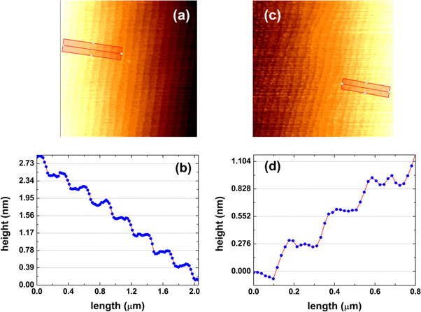
Figure 1. AFM images of BaBiO3 thin films grown on SrTiO3 substrates. (a) 5 × 5 μm2 image of 16 nm thick BaBiO3 film on SrTiO3 (001), (b) height scan along the line designated in (a). (c) 5 × 5 μm2 image of 17 nm thick BaBiO3 film on SrTiO3 (110), (d) height scan along the line in (c).
Download figure:
Standard image High-resolution imageWe next analyze the crystalline structure of various BaBiO3 thin films on MgO and SrTiO3 substrates; the XRD patterns of the films are displayed in figure 2. (BaBiO3 and SrTiO3 are designated as BBO and STO, respectively, in this figure and thew following ones.) It may be noted that there exists an overall mismatch of about 10% in the lattice constant of BaBiO3, 0.4337 nm for bulk [17], to that of SrTiO3, 0.3905 nm while there is only a 3% difference in the case of MgO with 0.4210 nm. Nevertheless, it is seen from the XRD data that the films are well in epitaxy with the underlying substrates. In figure 2(a) the XRD pattern of a 16 nm thick film on SrTiO3 (001) is shown; the film thickness is obtained from low angle x-ray reflection (XRR) measurements. The inset is the theta rocking curve measured at the (001) peak with FWHM = 0.077° from a Gaussian line fit. Similarly, figure 2(b) is the XRD pattern of a 9 nm thick film on a SrTiO3 (110) substrate and figure 2(c) is for a 88 nm thick film on MgO (100). Reciprocal space mapping (RSM) is also carried out at Pohang Light Source; figures 2(d) and (e) are the detailed RSM results for a 44 nm film on SrTiO3 around the SrTiO3 (103) peak and for a 88 nm film on MgO measured at the MgO (113) peak, respectively. X-ray energy is calibrated with substrate peak with relative energy resolution of dE/E ∼ 10−4 under the assumption that bulk substrate is an infinite ideally perfect crystal. It is seen from figure 2(e) that the peaks from the film and the underlying substrate are in close proximity and thus the film on MgO (100) is in registry with the substrate. For the BaBiO3 film on SrTiO3 (001), on the other hand, it appears relaxed due to the lattice constant mismatch and the film peak and the substrate peak in the reciprocal space are not at all in proximity. In this case, two separate measurements were needed to cover the relevant reciprocal space region as shown in figure 2(d).
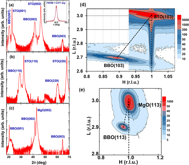
Figure 2. XRD patterns of BaBiO3 thin films on MgO and SrTiO3 substrates. (a) θ−2θ scan for BaBiO3 film on SrTiO3 (001). The inset shows a theta rocking curve for film (001) peak. (b) θ-2θ scan for BaBiO3 film on SrTiO3 (110). (c) θ-2θ scan for BaBiO3 film on MgO (100). (d) RSM for 44 nm thin BaBiO3 film on SrTiO3 (001) around the SrTiO3 (103) peak. (e) RSM for 88 nm thin BaBiO3 film on MgO (100) around the MgO (113) peak.
Download figure:
Standard image High-resolution image4. Physical properties of epitaxial BaBiO3 films
4.1. Raman scattering measurements
Our main interest towards BaBiO3 epitaxial thin films is how their physical properties would differ as orientation as well as strain vary. For this purpose, we first resorted to light scattering measurements of the thin films because the Raman modes of BaBiO3 would be sensitive to strain variation. Structural distortion, which connects the ideal cubic structure to the observed distorted structure, can be identified as a symmetry breaking element of displacive nature, either polar or non-polar, leading to distinct electromagnetic responses. For BaBiO3 the most distorted structure is monoclinic with symmetry group P21/n; for the transition from ideal cubic  to monoclinic P21/n, two symmetry modes,
  and
and  are involved [9].
  corresponds to out-of-phase tilting along the pseudo-cubic [110] axis while
  is the mode responsible for in-phase tilting along the pseudo-cubic [010] axis. Both of these modes are non-polar, and the distortion can be understood in terms of the octahedral tilting only. At room temperature BaBiO3 belongs to another monoclinic I2/m (a−a−c0) with out-of-phase tilting along the [110] direction; in the monoclinic phase, Raman active optical phonon modes are
  [18, 19].
Figure 3 shows Raman scattering spectra for the films on MgO (100) and SrTiO3 (001) substrates. With the help of the reported optical data [20], we are able to assign the peaks in the Raman spectra as the OT modes (Bi–O bending and Bi–O stretching) and the OB (BiO6 breathing) mode from low to high energy values. Specifically, the strongest Raman peak at 565 cm−1 is due to the BiO6 breathing with Ag symmetry [21], the peak at 492 cm−1 is assigned to the Bi–O stretching mode, and the one around 300 cm−1 is the superposition of the multiple Bi–O bending modes as designated in figure 3(a). 2nd order peak also appears around 1130 cm−1. For the multiply superposed bond bending peak in the vicinity of 300 cm−1 whose details are displayed in figures 3(b) and (c), the spectral line at 298 cm−1 would be due to the out-of-phase Bi–O bending with Ag symmetry while the mode at wave number 314 cm−1 may be assigned to the Ag symmetric in-plane mixed vibrations of Bi and O atoms. The peaks at 342 cm−1 and 347 cm−1 are due to the out-of-phase bond bending with Bg symmetry. From figure 3(b) for the relaxed film on SrTiO3 (001), it is of interest to note that the Ag symmetric in-plane vibrational mode at 314 cm−1 has a higher intensity and a narrower width than the out-of-phase bending mode at 298cm−1. In addition, a broad spectral line with Bg symmetry appears at 342 cm−1. It is also noted from figure 3(c) that the strained film on MgO (100) gives rise to a narrower linewidth and a higher intensity at 299 cm−1 than at 314 cm−1 and only a very small Bg mode at 347cm−1 is seen. These results would imply that in-plane bond bending is restricted in strained films and thus a shortened phonon lifetime and a broader linewidth would follow. Again it is recalled that BaBiO3 with lattice constant a = 0.4338 nm has 3% lattice mismatch with MgO (a = 0.421 nm) whereas 10% with SrTiO3 (a = 0.395 nm). In particular, a large mismatch between BaBiO3 and SrTiO3 would cause relaxation; indeed, BaBiO3 films grown on SrTiO3 (001) are fully relaxed while the films on MgO (100) are strained. It is mentioned in passing that Inumaru et al claimed a partial suppression of the OT modes for BaBiO3 films grown on MgO substrates [13], and, in contrast, local breathing and tilting distortions were reported even for superconducting Ba1−xKxBiO3 and BaPb1−xBixO3 films on SrTiO3 substrates [22].
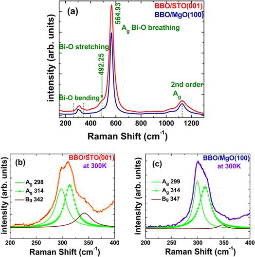
Figure 3. Room temperature Raman spectra for BaBiO3 films. (a) Comparison of 200 nm BaBiO3 film on SrTiO3 (001) (red line) with 84 nm BaBiO3 film on MgO (001) (blue line). (b) & (c): The broad Raman peaks around 300 cm−1 for BaBiO3/SrTiO3 (001) and BaBiO3/MgO (001) films, respectively, are analyzed with the superposition of multiple Lorentzian lines.
Download figure:
Standard image High-resolution imageTo monitor the changes in the tilt pattern of BaBiO3 in association with the structural tranistion around 140 K, Raman scattering measurements were performed, as a function of temperature ranging from 50 K to 300 K, on the films on SrTiO3 substrates with (001) and (110) orientations. The broad peak in the vicinity of 300 cm−1 is analyzed in terms of the superposition of multiple Lorentzian lines and the results are displayed at various temperatures in figures 4(a) and (b). As can be seen from the figures, there is a significant change in the superposition contents of the modes below and above the transition temperature. The structural transition from monoclinic P21/n (a−a−c+) to monoclinic I2/m (a−a−c0) occurring at temperature 140 K upon raising temperature is known to be an octahedral tilt-driven continuous transition [7]. From figures 4(a) and (b), it is immediately obvious that the vibrational modes of Ag symmetric 306 cm−1 and Bg symmetric 352 cm−1 appear only in the low temperature phase; in-phase rotation of the BiO6 octahedra around the c-axis would induce such modes. In figure 4(c), there is not too much change in the energy shift for the observed Raman modes except for Ag symmetric in-plane vibrational mode at 314 cm−1 which shows hardening on cooling. The peak intensity of the Ag symmetric 306 cm−1 mode increases with lowering temperature for the film grown on SrTiO3 (110) substrate as can be seen from figure 4(d). The intensity of all other modes decreases with decreasing temperature. The spectral width of a line in the Raman spectrum is a measure of the phonon lifetime. With the in-phase rotation around c-axis at transition temperature 140 K, the width of the Bg modes at 342 cm−1 and 352 cm−1 broadens with decreasing temperature. It is also seen from figure 4(d) that there is a difference in the spectral features depending on the orientation; the film with (001) orientation shows low scattering intensity for the 314 cm−1 mode compared to the film with (110) orientation in the low temperature phase. It may be recalled that a BaBiO3 film grown with (001) orientation was reported to have a tetragonal structure [14]; an elongation in the c-axis would release the out-of-phase octahedral tilting along the [110] axis, corresponding to the in-plane vibrational mode at 314 cm−1, and this could be a reason for the lower intensity of the 314 cm−1 mode for the film on SrTiO3 (001) compare to the film with (110) orientation.
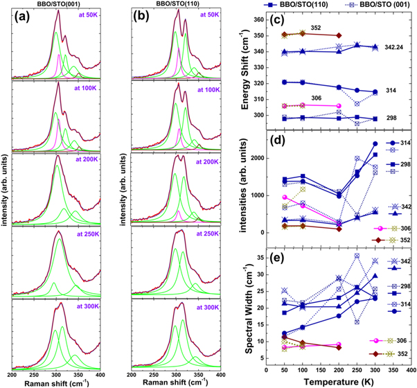
Figure 4. Temperature effects on the Raman modes around 300 cm−1 for BaBiO3 films grown on SrTiO3-substrates. (a) Raman spectra at various temperatures for 200 nm thick BaBiO3 film on SrTiO3 (001). The broad peak is decomposed into constituent Raman modes. (b) For 200nm BaBiO3 film on SrTiO3 (110). (c)–(e): The energy shift, intensity, and spectral line width of the decomposed Raman modes are plotted as a function of temperature.
Download figure:
Standard image High-resolution image4.2. Dielectric constant measurements
We next turn to dielectric measurements of BaBiO3 films. BaBiO3 is considered to be a semiconducting material because it has a band gap arising from the CDW [10, 23]; using the 2-probe method, we measured the surface resistance of a BaBiO3 film and found it to be 16 MΩ at 300 K. In general, disorder inevitable even in crystalline samples causes the occurrence of localized states, and electrons could be trapped in the localized states. Random thermal fluctuations would then give electrons enough energy to get out of a localized state and move to a near one by hopping, that is, electrons move, for a brief amount of time, before relaxing into another localized state. For BaBiO3, conduction would be possible due to hopping of 6 s electrons on the localized states and this behavior could lead to relaxation phenomena. Furthermore, charge disproportionation in two adjacent B-site Bi ions in distorted BaBiO3 might give rise to a local electric dipole that can absorb electromagnetic energy depending on measuring field frequency and temperature.
We grew BaBiO3 films on conducting substrates, 5 wt% Niobium doped SrTiO3 in (001) and (110) orientations, and out-of-plane dielectric measurements were taken in a vertical capacitor arrangement as sketched in figure 5(a). Top electrodes were deposited with gold in a thermal evaporation chamber. For quantitative analyses with regard to the orientation dependence, we covert the raw data to complex dielectric constant of intrinsic nature without geometric dependence of measuring devices. In the vertical configuration as in the present case, it is straightforward to obtain ε'; real part and ε''; imaginary part of the complex dielectric constant from the raw data [24]:


where Cx is the measured capacitance value for material,  is the loss tangent, d is the thickness of a film, A is the area of the electrode, and
  is the permittivity of free space.
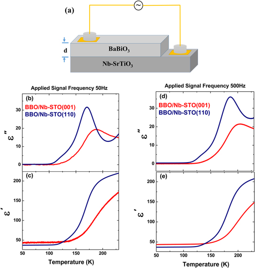
Figure 5. Out-of-plane dielectric measurements of BaBiO3 films. (a) Measurement setup for a film with thickness d. Real (ε') and imaginary (ε'') parts of dielectric constant as a function of temperature for 200 nm thick BaBiO3 films, (b), (c) applied signal frequency at 50 Hz and (d), (e) at 500 Hz respectively. Red lines denote BaBiO3 on Nb-SrTiO3 (001), and blue lines represent BaBiO3 on Nb-SrTiO3 (110).
Download figure:
Standard image High-resolution imageFor 200 nm thick BaBiO3 films on Nb-doped SrTiO3 (001) and (110), ε' and ε'', obtained from the data measured at applied signal frequencies of 50 and 500 Hz, are plotted against temperature in figures 5(b)–(e). The structural transition of BaBiO3 from monoclinic-I (P21/n) to monoclinic-II (I2/m), occurring around 140 K on increasing temperature, is associated with a large abrupt change in dielectric constant ε' from a low value to a large value [7].
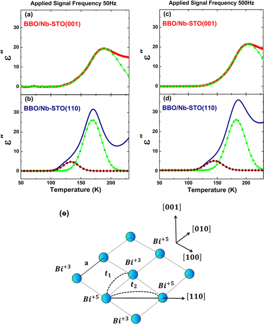
In figures 6(a) and (c) imaginary part of dielectric constant ε'' is plotted against temperature for BaBiO3 film on Nb-doped SrTiO3 (001) measured at frequencies of 50 and 500 Hz, respectively, with a fitting curve. Only one broad relaxation peak is observed here, and the fitting curve is from a Gaussian distribution of relaxation times. In contrast, for a 200 nm thick film on Nb-doped SrTiO3 (110), ε'' again obtained at measuring frequencies of 50 and 500 Hz, behave quite differently from the case of the (001) orientation as can be seen from figures 6(b) and (d). The imaginary part ε'' in particular can be considered to consist of two broad relaxation peaks, one peak around 140 K and another one around 180 K. The fitting curves in figures 6(b) and (d) are again from the Gaussian distribution of relaxation times. In BaBiO3, Bi 6s and O 2p orbitals form an electronic band near the Fermi level, i.e., the conduction band. Lattice distortions in the perovskite structure would modify the conduction properties of BaBiO3; the breathing distortion opens the charge gap while the tilting distortion causes an overall band narrowing [25]. To hybridize with Bi 6s orbitals, only O 2pδ orbitals with A1g symmetry are allowed. For low energy electronic excitations in BaBiO3, Khazraie et al estimated effective hopping integrals for nearest neighbor and next nearest neighbor using a single orbital tight binding model [26]. They showed that with the breathing distortion of  and no external electric field, the size of the hopping integral t1 between nearest neighbors involving oxygen atoms with A1g symmetry is four times larger than that of the next nearest neighbor hopping integral t2 between two Bi ions sit at a distance
  as shown in figure 6(e). The difference in the relaxation behaviors of BaBiO3 films with orientations (001) and (110) may be due to the difference in the relative contributions of hopping integrals, i.e., t1 alone vs both t1 and t2 depending on the direction of an applied electric field. When an applied electric field is parallel to the [001] axis, only t1 contributes whereas both hopping integrals, t1 and t2, contribute when E // [110], leading to two relaxation peaks as observed experimentally. It is also noted that the relaxation peak height due to t2 in figures 6(b) and (d) is about 1/4 less than that due to nearest neighbor hoping t1; in fact, this quantitative difference was already demonstrated by the calculation in 26.
Figure 6. Curve fitting analysis of the Imaginary part ε'' of complex dielectric constant of BaBiO3 films. For 50 Hz applied signal frequency ε'', with a Gaussian fit, are shown against temperature for BaBiO3/Nb-SrTiO3 (001) and (110) in (a) and (b) and for 500 Hz signal frequency in (c) and (d) respectively. (e) Hopping integrals for nearest and next nearest neighbor in BaBiO3 are shown.
Download figure:
Standard image High-resolution image
5. Conclusion
We have grown BaBiO3 films epitaxially on MgO (100) and SrTiO3 (001) and (110) substrates using pulsed laser deposition. X-ray diffraction and reciprocal space mapping show that the thin films are grown epitaxially but relaxed considerably particularly for the films on SrTiO3. The topography of the film surfaces is found to be atomically flat with the step and terrace structure of unit cell step height. Raman spectroscopy measurements on strained BaBiO3 films grown on MgO (100) substrates reveal the restriction effect on in-plane Bi–O bond bending. In the temperature range from 50 K to 300 K, it is observed that the number of the vibrational modes is different for the two phases below and above the structural transition temperature around 140 K. The broad peak in the Raman spectra of BaBiO3 is decomposed into the multiple vibrational modes. Dielectric measurements reveal the frequency and orientation dependence of the dielectric constant and loss of BaBiO3 films. The dielectric measurements expose that the hopping processes for 6s electrons are different for different crystallographic orientations. In the present publication, we have tried to shed new light on the structural distortions, octahedral tilting effects, and electronic properties of BaBiO3 using epitaxial thin films with different strains and orientations.
Acknowledgments
We thank Eun Soo Ahn, and Sang Woo Kim for the assistances in measurements and Abhijit Biswas and Alireza Kashir for helpful discussion. We would like to thank Prof. Yoon H Jeong for the guidance in carrying out the whole experiment. Reciprocal Space Mapping (RSM) measurements were performed at beam line 3A of the Pohang Light source (PLS). This work was supported by National Research Foundation (NRF) of Korea (2015R1D1A1A02062239 and 2018R1A6075964).