

Abstract
Due to their outstanding electronic and physical properties, two-dimensional (2D) materials have attracted much interest for the fabrication of solid-state microelectronic devices. Among all methods to synthesize 2D materials, chemical vapor deposition (CVD) is the most attractive in the field of solid-state microelectronics because it can produce high quality 2D material in a scalable manner. However, the high temperatures (>900 °C) required during the CVD growth of the 2D materials impede their direct synthesis on metal-coated wafers due to prohibitive metal diffusion and de-wetting. This makes necessary carrying out the 2D materials CVD growth independently on metallic foils, and transfer them on the wafers using polymer scaffolds. However, this process is slower, more expensive, and can lead to abundant contamination and cracks in the 2D material. Here we present a facile method to allow the direct growth of multilayer hexagonal boron nitride (h-BN) on Ni-coated Si wafers, which consists on placing a protective cover 30 μm above the Ni surface. The resulting h-BN stacks have been used to fabricate Au/Ti/h-BN/Ni memristors with low cycle-to-cycle variability. This work contributes to the integration of 2D materials in solid-state micro- and nano-electronic technologies.
Export citation and abstract BibTeX RIS
The introduction of layered two-dimensional (2D) materials in the structure of electronic devices is an interesting strategy to enhance their performance and provide additional functionalities. For example, graphene (which is conductive) has been used as electrode in capacitors [1] and batteries [2], and transition metal dichalcogenides (TMD), such as MoS2, WS2 and WSe2 (which are semiconducting), are often used as channel in field-effect transistors (FET) and photodetectors [3–5]. Hexagonal boron nitride (h-BN) is a 2D layered material made of B and N atoms arranged in an sp2 hexagonal lattice that has a band gap of 5.9 eV [6]. Therefore, h-BN is an electrical insulator, and it can be very useful for many different applications. So far, h-BN has been proved to be a very reliable gate dielectric for FETs and can resist electrical stresses much better than high-k dielectrics [7, 8], as well as serving as a versatile resistive switching (RS) layer for memristors [9–11]. Moreover, h-BN can be used as substrate for epitaxial growth of graphene to form van der Waals heterostructures [12], as its lattice parameters are very similar to those of graphene. In fact, h-BN has been used as anti-scattering substrate for graphene and MoS2 based devices [13, 14], as it produces a very good interface free of dangling bonds with all other 2D materials. Reference [15] fabricated h-BN encapsulated graphene FET's via mechanical exfoliation, in which the top h-BN serves as gate dielectric and the bottom h-BN as anti-scattering substrate.
However, the main problem hindering the introduction of 2D materials in electronic devices is their synthesis [16]. Mechanical exfoliation is a very common way to synthesize high quality 2D materials for research purposes, but it can only produce small flakes (<20 μm) with thickness fluctuations [17]. Liquid-phase exfoliation (LPE) can be used to produce thick (>50 nm) h-BN dielectric meshes made of multiple flakes aggregated and with random orientations [18]. However, LPE films of 2D materials are much rougher and allow much more charge and ionic transport across the junctions between different nanoflakes [19], which are two effects specially unwanted in a dielectric. As an example, LPE 2D dielectrics for memristors show a very poor endurance [20]. Other scalable methods to produce h-BN are: molecular beam epitaxy (MBE) [21], physical sputtering (PS) [22], and chemical vapor deposition (CVD) [23]. In these three methods the h-BN is grown by the bottom-up nucleation of molecules containing B and N atoms, which requires the use of a metallic catalytic substrate. h-BN sheets grown by these methods present more lattice defects than exfoliated ones, but their quality may be still acceptable for some electronic devices. As an example, by using only CVD-grown 2D materials, reference [24] developed h-BN encapsulated graphene FET's, similar to those fabricated by mechanical exfoliation in reference [15]. Recently, reference [25] used CVD-grown h-BN to fabricate memristors with potential applications as electronic synapses.
However, the main problem of MBE, PS and CVD approaches is that they require the use of high temperatures (>850 °C), which can damage the substrates on which they are grown due to severe diffusion and de-wetting (i.e. the temperatures used in back-end-of-line microelectronic processes are always <400 °C [26])—the term substrates in this sentence refers to the wafers containing structures and/or electronic devices patterned before the 2D material growth. For this reason, the h-BN sheets synthesized by these methods almost always use an independent substrate for the growth, typically a metallic (Cu [23], Ni [27], CuNi [28], Pt [6], Fe [29]) foil, and subsequent transfer of the h-BN sheets onto the target wafers to build devices. However, this process is slow and requires human labor (i.e. it is expensive), can easily produce cracks in the h-BN sheet, and often leads to contamination from polymer scaffolds [30].
Very few authors tried to directly grow h-BN on metal coated wafers, and most of them used CVD approach due to its lower cost, easier setup, and higher quality compared to MBE and PS. References [31, 32] used a cold-wall CVD furnace to grow h-BN on Fe, Ni and Co coated Si wafers, and the growth was enabled by diffusion and segregation mechanism. References [27, 33] used atmospheric pressure CVD to grow h-BN on Ni coated Si wafers, and the growth was enabled by (i) polymerization of borazine to form poly-borazylene, which was subsequently dehydrogenated to form h-BN [27], and (ii) metal atomic vacancy-assisted B-N molecular diffusion [33]. References [34, 35] used vacuum anneal method to grow h-BN on Ni, Co and NiFe coated Si wafers using a seed amorphous BN (a-BN) film between the metal and the Si wafers. In this case the growth was enabled by segregation of B and N atoms across the metallic film, i.e. from the a-BN source onto the surface of metal film. However, this setup is more complex and costly, due to the need of a high vacuum chamber (5 × 10⁻⁵ Pa).
Despite these advances, most of these works concentrated on studying the properties of the material using different characterization tools, such as scanning electron microscopy (SEM), transmission electron microscopy (TEM), and Raman spectroscopy, and there was no direct use of the h-BN grown on metal coated wafers to build any kind of device. The only effort in this direction was reported in reference [32], which built a graphene FET on the h-BN; however, in that work the h-BN was used as anti-scattering substrate, not as dielectric. So far, we are not aware of any work demonstrating the fabrication of electronic devices using h-BN dielectric stacks directly grown on metal coated wafers.
Here we show the direct synthesis of h-BN stacks on metal coated wafers using a standard CVD system, and we demonstrate the fabrication of metal/h-BN/metal memristors exhibiting bipolar resistive switching (RS). The successful h-BN synthesis on the metal coated SiO2/Si wafer (substrate) was enabled by placing another SiO2/Si wafer (protective cover) exactly on it [36], which reduced the amount of gas arriving to the surface of the Ni and avoided severe diffusion and de-wetting.
300 nm SiO2/Si wafers were coated with ~700 nm Ni films in a magnetron sputtering system (Kurt J. Lesker, PVD75), at room temperature under 5 mTorr Argon gas atmosphere. The radiofrequency power used was 150 W, and the deposition rate was 0.5 Å s−1. The Ni source was purchased in Zhongnuo New Materials (purity 99.995%). Figure 1(a) shows the cross sectional SEM image of a Ni/SiO2/Si wafer. As it can be observed, the Ni film contains vertical/parallel elongated grains. Initially we also used Ni/SiO2/Si wafers fabricated by electron beam evaporation; however, evaporated samples were discarded due to severe inhomogeneities after the annealing process.
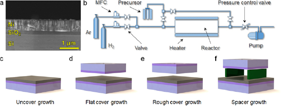
Figure 1. (a) Cross-sectional SEM image of the 700 nm Ni/300 nm SiO2/Si substrates used in this investigation. (b) Schematic of a low pressure CVD system used in this investigation. In order to avoid Ni de-wetting, the Ni/SiO2/Si substrates have been protected with a cover before introducing them in the CVD system for annealing and h-BN growth. We used three different types of covers: one with a flat surface (d), one with a rough surface (e), and one flat using spacers (f); these three configurations result in a cover/substrate gap of ~12.5 μm, ~30.5 μm, and >500 μm (respectively). More details about the covers and gaps are given in supplementary figure 1. Controlling the height of this gap is important in order to tune the amount of H2 gas and precursor reaching the surface of the Ni film. (c) One sample without any cover has been used as reference. MFC applies to mass flow controller.
Download figure:
Standard image High-resolution imageThe Ni/SiO2/Si wafers were cut in small pieces (1.2 cm × 1.2 cm) and introduced in the center of the quartz tube of the CVD furnace (diameter of 2.5 cm), following one of the four configurations indicated in figures 1(c)–(f). Then, the pressure of the chamber was pumped down to ~1 mTorr, a flow of 5 sccm H2 was introduced into the tube, and the temperature of the CVD system was increased to 1050 °C for thermal annealing. Ramping up the temperature to 1050 °C took 25 min, and it was maintained at this value for different times of 1, 5, 10, 30, 60 and 90 min (namely, annealing time). After that the h-BN films were grown by introducing ammonia borane precursor into the tube. The ammonia borane precursor was solid state, and it was heated at ~90 °C using a separated chamber to partially evaporate it. The precursor was introduced in the tube furnace using a different line. A flow of 50 sccm H2 was introduced to carry evaporated precursor. We tried different growth times of 1, 5 and 10 min. After that, the valve controlling the precursor flow was closed, and the CVD furnace was cooled down to room temperature (still under 5 sccm H2 flow). Finally, the H2 flow was switched off and the h-BN/Ni/SiO2/Si samples were extracted.
The main peculiarity of our CVD process is that we used four different sample configurations (in the tube furnace) during the annealing and growth in order to tune the amount of precursor and H2 gas arriving to the surface of the Ni/SiO2/Si substrate. Driving the precursor to specific parts of the substrate may allow controlling the properties of the 2D materials. For example, in reference [37] the authors grew graphene via CVD by using a pipette to introduce carbon precursor locally exactly in the center of the sample, leading a single seed that produced centimeter scale single crystalline graphene sheets. In our case, as the main problem is the de-wetting of the Ni film, we placed a protective cover right resting over the Ni/SiO2/Si substrate (without using any adhesive), and by tuning the distance between them we have been able to control the amount of H2 and precursor arriving to the Ni surface. The schematic of the CVD system used is displayed in figure 1(b), and figures 1(c)–(f) show the four different sample configurations used. Initially we used two types of covers: (i) one with a very flat surface (see figure 1(d)) with roughness <0.186 nm (as measured by AFM, see figure S1(a)). This cover was basically the polished side of a commercial SiO2/Si wafer. Despite this cover was resting exactly on the Ni/SiO2/Si substrate at several locations a small gap of typically ~12.50 μm was detected between them (see figure S1(b)). And (ii) one with a rough surface (see figure 1(e)), as observed by SEM (see figure S1(c)). This cover was basically the unpolished side of a commercial SiO2/Si wafer. The larger roughness of this cover increased the gap up to ~30.5 μm at several locations (see figure S1(d)). Finally, the gap between the Ni/SiO2/Si substrate and the cover was further increased by introducing two spacers (i.e. small pieces of SiO2/Si wafer), which increased the gap to ~500 μm (see figure 1(f)).
In order to characterize the morphology of the Ni films after the annealing (which may have an important effect during the h-BN growth) in some cases the process was stopped right after the annealing step, i.e. the CVD furnace was cooled down to room temperature without having introduced the precursor, and the Ni/SiO2/Si samples were extracted for exhaustive characterization. More specifically, the fresh Ni/SiO2/Si samples (figure 2(a)) were introduced in the CVD furnace for thermal annealing at 1050 °C during 5 min, first without any cover (figure 2(b)) and later using a flat cover (figure 2(c)). As it can be observed, in both cases the Ni film became polycrystalline due to the high temperatures (as expected); this effect can be better distinguished from the corresponding SEM images (figures 2(e) and (f)). The interesting and unexpected observation is that the samples covered always show a much larger grain size than uncovered ones. The morphology of the annealed Ni/SiO2/Si using the flat cover (figure 2(c)) is more suitable to grow h-BN than the uncovered one (figure 2(b)), because it is smoother and has larger grains, which may reduce the amount of defects in the h-BN stack [6]. Therefore, reducing the number of metal grains by increasing their size is desirable. The size of the Ni grains can be slightly increased by enlarging the annealing time (see figure 2(d)). A detailed statistical analysis of the grain size depending on the annealing temperature is shown in the supplementary information (see figure S2 (stacks.iop.org/TDM/6/035021/mmedia)). However, for annealing times above 5 min, the grain size improvement at longer times is not significant and it does not justify the additional energy and time consumption. Therefore, we decided to grow the h-BN using an annealing time of 5 min.
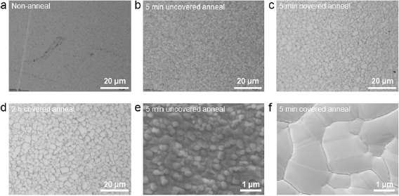
Figure 2. Optical microscope photographs of the Ni/SiO2/Si substrates at different process stages: (a) before any thermal treatment (i.e. after Ni film deposition), (b) annealed without cover for 5 min, and (c) and (d) annealed using a flat cover for 5 min and 2 h (respectively). (e) and (f) Scanning electron microscopy images showing the surface morphology of the samples in (b) and (c), respectively.
Download figure:
Standard image High-resolution imageIn the next step, the growth of the h-BN has been carried out using the four configurations displayed in figures 1(c)–(f) (i.e. uncovered, flat cover, rough cover and spacer cover). Figure 3 shows the top SEM image of each sample after the h-BN growth. When no cover is used the surface of the Ni film is severely damaged due to diffusion and de-wetting (figure 3(a)). In fact, this is one of the main problems hindering the growth of 2D materials on metal coated wafers using standard CVD systems: references [27, 31–35] used customized CVD systems, not standard ones. When a flat cover is used no h-BN on the Ni film has been detected. This can be seen from the absence of Raman peaks in the range from 1300 cm−1 to 1500 cm−1 (see figure 3(e), black line). Most probably the small gap of 12.5 μm between the Ni/SiO2/Si sample and the flat cover was too narrow and impeded enough precursor molecules to reach the Ni film. On the contrary, when using the rough cover good h-BN coverage has been observed (figure 3(c)), and the Raman signal shows a peak at 1368 cm−1, which is characteristic of multilayer h-BN stacks [38] (figure 3(e), blue line). Indeed, this result demonstrates that a gap of 30.5 μm between the Ni/SiO2/Si sample and the cover is enough to allow the flow of enough ammonia borane precursor between them. When using the spacer cover the surface of the h-BN also showed good h-BN signal in the Raman shift (figure 3(e) red line); however, abundant pinholes have been often observed in the SEM images at several locations of the sample (figure 3(d)), indicating that the larger distance to the cover (>500 μm) allowed too much H2 gas reach the Ni surface, which produced noticeable damage to it. We would like to highlight that the Raman spectra shown in figure 3 have been statistically corroborated at 15 different locations of each sample, and reasonable deviations have been observed. Nevertheless, as the ultimate application of the h-BN film in this study is to build memristors, and these need defects to be operated, the observation of inhomogeneity in the Raman signal from one location to another is not a concern [25]. Therefore, further variability analysis of the Raman signal using other advanced techniques such as Raman mapping, despite being useful, is not highly necessary.
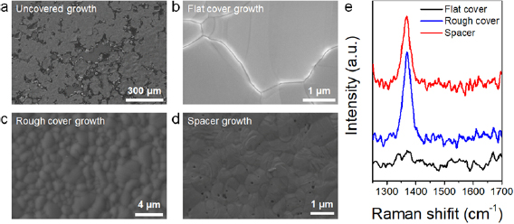
Figure 3. (a)–(d) SEM images of the surface of the Ni/SiO2/Si substrates after the h-BN growth using the four different configurations mentioned: (a) uncovered growth; (b) flat cover growth; (c) rough cover growth and (d) spacer growth. (e) Raman spectra collected on the surface of the sample after the h-BN growth process. Without cover the surface of the Ni experiences severe de-wetting (a). Using the flat cover does not produce h-BN growth, as seen by the missing peak in the Raman signal, see black line in panel (e). Probably the reason is the small gap (~12.5 μm) between the substrate and the cover. Using rough and spacer cover produces good h-BN signal, as shown in panel (e); however, the spacer cover leads to the formation of small pits on the surface of the wafers, probably due to the larger gap (>500 μm) between the substrate and the cover. The use of a rough cover seems to be the optimal solution to prevent Ni de-wetting and allow h-BN growth.
Download figure:
Standard image High-resolution imageIn the next step the Au/Ti/h-BN/Ni memristors have been fabricated by direct evaporation of 20 nm Ti and 60 nm Au, through a laser-patterned shadow mask (figure S3), on the h-BN stacks grown using a rough cover. The size of the memristors ranged from 100 μm × 100 μm down to 10 μm × 10 μm. Before electrical characterization, the morphology of the Au/Ti/h-BN/Ni memristors was analyzed by cross sectional TEM images, which revealed that the h-BN film grown is a truly layered stack, and that its thickness fluctuates between 10–12 layers (figure 4(a)). Proving a layered structure is essential to make sure that the film will hold some important properties characteristic of 2D materials that would be relevant for the performance of the memristors, such as high thermal conductivity.
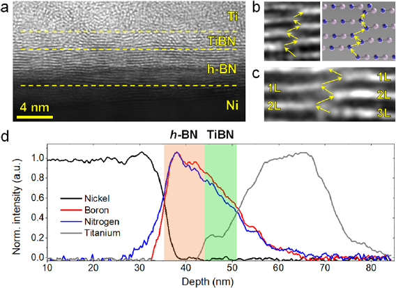
Figure 4. (a) Cross-sectional TEM image showing layered structure of the Au/Ti/h-BN/Ni memristors fabricated in this investigation. (b) 1.3 nm × 1 nm and (c) 1 nm × 2.4 nm zoom-in images of two defective regions in panel (a) displaying defective paths across the h-BN stack, which are originated by h-BN planes misalignments and/or bifurcations. The yellow arrows in (b) and (c) highlight the defective path facilitating leakage current across the h-BN stack. (d) EELS cross-sectional analysis showing the chemical composition of the Au/Ti/h-BN/Ni memristor. The progressive reduction of the B and N signals when approaching to the Ti electrode, and the plateau at the Ti signal between 44 nm and 48 nm indicate the formation of an effective TiBN layer.
Download figure:
Standard image High-resolution imageIt is worth noting that the h-BN/Ni interface is much sharper than the Ti/h-BN one, i.e. the first h-BN layer on the Ni film is continuous, while the last 3–4 h-BN layers close to the Ti electrode appear to be discontinuous, leading to thickness fluctuations ranging from 1 to 3 layers. This hypothesis has been corroborated by collecting cross sectional electron energy loss spectroscopy (EELS) profiles of the TEM images (see figure 4(d)). As it can be seen, the slope of the Ni profile is sharp, while the slope of the Ti profile is progressive. The B and N profiles show an asymmetric shape with a much more progressive slope at the Ti/h-BN interface. It is also striking that the B and N profiles closely overlap; normally B migration takes place at lower energies [39], which results in asymmetric B profiles, while the N profile normally remains symmetric due to the lack of N migration [9]. Therefore, it seems that a pseudo-amorphous TiBN layer may have formed exactly over the layered h-BN stack. This can be also seen by the plateau formed by the Ti signal at the TiBN layer (see figure 4(d), depth 44 nm to 48 nm). The top part of figure 4(a) also indicates that some of these B and N atoms within the TiBN layer may still retain their hexagonal bonding, leading to h-BN nanoflakes embedded.
The defective top interface of the h-BN stack may impede its use as anti-scattering substrate for graphene or MoS2 FETs. However, this type of defective interface may be beneficial for the fabrication of memristors, as it may promote RS by charge trapping and de-trapping at the defective sites. Moreover, it should be highlighted that the thickness fluctuations observed at the Ti/h-BN interface in figure 4(a) are much smaller than those observed in exfoliated samples [17], which is an immediate advantage to reduce the device-to-device variability.
By detailed analysis of the TEM images it can be observed that the h-BN stack also contains native defects within the bulk of the h-BN stack. Figure 4(c) shows the zoom-in TEM image of a defective area within the h-BN where two layers separate and become three. Interestingly, this transition generates a very narrow (<0.5 nm) out-of-plane defective path in the h-BN stack across which electrons may flow (see yellow arrows in figure 4(b)). Similar out-of-plane lattice mismatch and defective paths have been also detected at several locations of the samples (see figures 4(b) and (c)). It should be highlighted that the presence of local native defects in a dielectric promotes the formation of percolation paths at lower energies, leading to narrower conductive nanofilaments (CNF) that can be more easily disrupted [40, 41], favoring observation of RS. As an example, SiO2 grown via thermal oxidation (which contains low amount of native defects) does not show reliable RS, while SiO2 deposited via sputtering (which contains several defective grain boundaries) has shown excellent RS. Similarly, h-BN grown via mechanical exfoliation has never showed reliable RS, but CVD-grown (and transferred) h-BN has shown good RS behavior [25]. By statistical analysis of 5 TEM images that display the structure of the h-BN stack (with sub-nanometer resolution) along more than 130 nm, we conclude that the average distance between two defective paths across the h-BN stack is ~2 nm. This small distance is beneficial for device scalability, i.e. if one defective path is needed to induce RS, large distances between them may impede the fabrication of small devices.
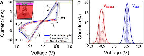
The electrical properties of Au/Ti/h-BN/Ni memristors (which in fact hold a Au/Ti/TiBN/h-BN/Ni structure, as shown in figure 4(d)) with size of 25 μm × 25 μm have been analyzed using a probe station connected to a semiconductor parameter analyzer. Sequences of current versus voltage (I–V) curves with different polarities have been applied to the top Au/Ti electrode, keeping the bottom Ni electrode grounded. The devices show correct bipolar RS with positive set and negative reset (figure 5(a)), and without the need of a forming process—the forming process is a step normally required by most transition metal oxide based memristors, in which the first I–V curve requires a much higher voltage to reach the first set transition; therefore, the fact that the Au/Ti/h-BN/Ni memristors here presented do not require this step is an immediate advantage that simplifies their programming. Interestingly, both the set and reset processes are smooth (see also figure S4), which is in contrast with previous observations of RS in h-BN based memristors [9, 10, 42, 43]. It should be highlighted that references [9, 10, 42, 43] used metallic foils for the CVD growth of the h-BN stack, not metal-coated wafers, and reference [43] used Ni as bottom electrode, suggesting that the progressive RS behavior observed in figures 5(a) and S4 may be linked to the direct CVD growth of h-BN on Ni coated wafers. We measured 100 RS cycles, and statistically analyzed the value of the set and reset voltages (VSET and VRESET, respectively). As figure 5(b) shows, the cycle-to-cycle variability is low, and comparable to that of memristors using high-k dielectrics [30].
Figure 5. (a) Typical I–V curves collected in a Au/Ti/h-BN/Ni memristor with size of 25 μm × 25 μm showing bipolar RS. The RS is forming free, and the set and reset transitions are progressive, suggesting the presence of interface phenomena. The inset shows the schematic of the Ti/TiBN/h-BN/Ni structure as simulated with the Ginestra™ multiscale modeling platform (the top Au capping electrode has not been included because its function is just to protect the Ti from oxidation). (b) Statistical analysis of VRESET and VSET in more than 70 cycles measured in the same device. The variability of VSET and VRESET, as well as that of IHRS and ILRS is similar to that of optimized transition metal oxide based memristors.
Download figure:
Standard image High-resolution image
These results have been observed in another 14 devices more with sizes of 25 μm × 25 μm, representing a yield of ~60%. It is worth noting that devices with larger areas of 100 μm × 100 μm showed a much lower yield <10%, i.e. most of the devices measured were initially shorted and do not show any sign of resistance recovery under reverse bias. This observation indicates the presence of some locations in the h-BN stack that are too defective and result in irreversible dielectric breakdown. However, as the size of real memristors required by the industry are always in the sub-micrometer range, this observation gives hope for future studies of smaller devices, and much higher yields for nanometric devices can be expected. In this proof-of-concept investigation, we did not fabricate smaller devices using cross-point or crossbar structure because we wanted to avoid transfer of the 2D material. Consequently, we used a configuration with bottom common in which the top electrode also serves as pad for the probe station (see figure S3). Because the radius of the probe station tip is not enough sharp and the microscope of any probe station has a limited resolution, the minimum size that could be contacted reliably was 25 μm × 25 μm. Future investigations should try to grow the h-BN stack via CVD on patterned metallic films that will serve as electrodes, instead continuous films. However, these structures may be less stable at high temperatures. In any case, such methodology represents next stage of complexity towards direct grow of 2D materials via CVD on metal-coated wafers, and it is out of the scope of this investigation. Apart from the higher yield for lower sizes, smaller devices are expected to drive lower currents in HRS (the currents driven in this state are normally area dependent) and have slightly larger VSET and VRESET (according to the percolation theory) [30].
Finally, the switching mechanism in the Au/Ti/h-BN/Ni memristors has been further studied by using a multiscale physical modelling platform called Ginestra™ [44]. This platform purposely accounts for the microscopic interactions and chemical reactions between electrons and atomic species (ions, vacancies, dangling bonds), to understand and engineer electron devices, connecting the microscopic properties of materials (including atomic defects, interfaces, morphology) to the electrical behavior of the device. In order to investigate the physical mechanisms responsible for the observed RS, the vertical structure of the device has been reproduced in the simulation environment by considering a Ni bottom electrode, a 3 nm-thick h-BN layer (representative of 10 stacked h-BN layers), an additional thin TiBN layer, and a Ti top electrode. The forming-less feature of these devices, besides being a concrete advantage from the operational standpoint, also suggests that the RS may be supported by native defects already present in the structure, like those constituting the critical highly defective locations evidenced in figures 4(b) and (c), which are typical formed as complementary pairs (i.e. so called Frenkel pairs). Since such locations are spatially distributed in the device, they may act like multiple localized CNFs, and the observed RS characteristic may arise from their partial disruption (because of the field-assisted recombination of the defects with their complementary species during the reset operation) and restoration (due to the field-assisted bond breakage and defect generation during the set operation). To verify this idea, we included in the simulated device a population of defects having an energy level uniformly distributed in the 2.5 ± 0.5 eV range below the conduction band of the h-BN, with a relaxation energy of 1.5 eV. The latter parameter is crucial to properly take into account the electron–phonon interactions that is at the core of the non-radiative multi-phonon trap-assisted tunneling that dominates the defect-assisted current through such dielectric materials [45]. To reproduce the I–V characteristic in LRS, we distributed the defects selectively in space, to mimic the existence of many narrow CNFs across the device (one of which is schematically shown in the inset of figure 5(a)), and adopted a large defect density value (i.e. 1022 cm−3). It has to be noted that this value is in between the accepted values for the density of oxygen vacancy defects in the broken part of the conductive filament (in HRS) and in the full conductive filament (in LRS) for HfO2-based RRAM devices [46]. The reset process is successfully simulated, as shown in figure 5(a), by considering the field-enhanced diffusion of the complementary defect species (in green in the inset of figure 5(a)) and their recombination with the defects forming the CNFs (in red in the inset of figure 5(a)). A vertical diffusion barrier of 0.4 eV and a lateral diffusion barrier of 0.8 eV were used, together with a field acceleration factor of 0.8 eÅ, while the recombination activation energy was set to 0.5 eV. The set operation is also successfully simulated by considering the field- and temperature-assisted defect Frenkel pairs generation (modeled in the framework of the McPherson thermochemical model [47]), using a generation activation energy of 1.6 eV, and a polarizability of 7.5 eV. Notably, these values are in reasonable agreement with previous studies on switching RS observed in h-BN [11], which adds up to the dependability of the results reported in this study.
In conclusion, h-BN stacks have been successfully grown by CVD method directly on metal coated wafers. The key factor avoiding severe metal diffusion and de-wetting at the high temperatures used during the CVD growth is the use of a flat cover placed directly on top of the Ni coated Si wafer. Essentially, the cover reduced the amount of gases arriving to the surface of the Ni, which produced larger Ni grains after the annealing, and a more controllable h-BN growth (as demonstrated via SEM and Raman spectroscopy). Transfer-free Au/Ti/h-BN/Ni memristors have been fabricated by direct evaporation of Au/Ti top electrodes on the h-BN/Ni/Si wafers. Interestingly, the memristors showed progressive RS without the need of a forming step, something very difficult to achieve using transition metal oxide RS media. By using cross-sectional TEM images coupled with EELS and multiscale modelling, we conclude that the RS is enabled by the formation of a defective TiBN film at the Ti/h-BN interface, as well as due to the formation of native percolation paths across the h-BN stack.
Acknowledgements
This work has been supported by the Young 1000 Global Talent Recruitment Program of the Ministry of Education of China, the Ministry of Science and Technology of China (grant no. BRICS2018-211-2DNEURO), the National Natural Science Foundation of China (grants no. 61502326, 41550110223, 11661131002, 61874075), the Jiangsu Government (grant no. BK20150343), the Ministry of Finance of China (grant no. SX21400213) and the Young 973 National Program of the Chinese Ministry of Science and Technology (grant no. 2015CB932700). The Collaborative Innovation Center of Suzhou Nano Science & Technology, the Jiangsu Key Laboratory for Carbon-Based Functional Materials & Devices, the Priority Academic Program Development of Jiangsu Higher Education Institutions, and the 111 Project from the State Administration of Foreign Experts Affairs are also acknowledged. D.A acknowledges the PECASE award through the Army Research Office.