
Abstract
In recent years, the realm of terahertz (THz) has seen a new paradigm of unprecedented development and offered new possibilities to strengthen the communication sector by studying the dielectric properties of different materials. The aim of this article is to present a comprehensive review of various THz technologies that have been employed to investigate the intrinsic characteristics of different materials. In addition, the study highlights the significance use of THz wave guides with some discussion on sources, and detectors and components. Towards the end, it highlights the future trends of THz technology and the challenges. The paper concludes that THz technology has a promising potential and offer new opportunities for applications in characterization of composite materials.
Export citation and abstract BibTeX RIS

Original content from this work may be used under the terms of the Creative Commons Attribution 4.0 licence. Any further distribution of this work must maintain attribution to the author(s) and the title of the work, journal citation and DOI.
1. Introduction
In the electromagnetic spectrum, the frequency range of 0.1–10 THz, the working wavelength of 30 μm – 3 mm between the electromagnetic wave is called teraher tz wave, which is between the infrared and microwave electromagnetic wave. In recent years, terahertz technology has been payed the attention to by many researchers due to its great research value and application prospect in the fields of next generation wireless communication [1–13], non-destructive security inspection [14–19], biomedicine [20, 21], food and agricultural product safety detection [22–26], global environmental monitoring [27–30], industrial applications [31], defence [32], and so on. Figure 1 shows the frequency & wavelength fields of the electromagnetic spectrum. Figure 2 shows that the terahertz technology is applied in some fields.
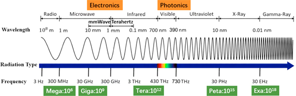
Figure 1. Frequency & wavelength fields in the electromagnetic spectrum.
Download figure:
Standard image High-resolution image
Figure 2. Terahertz technology applications.
Download figure:
Standard image High-resolution imageHowever, the development of terahertz technology is severely limited by the serious attenuation of THz wave in air and traditional materials due to the lack of materials that respond effectively to terahertz wave in nature. Firstly, this paper mainly describes the composition and application system of THz. Secondly, the THz detection method is discussed. Thirdly, the THz material problem is classified and described. Fourthly, the limitations and future trends of THz technology are discussed.
The design of this paper is as follows: section 1 is a brief introduction of terahertz. Section 2 discusses terahertz components and application systems. Section 3 gives terahertz detection methods and technologies. Section 4 describes terahertz material research. Section 5 proposes limitations of technology and future application trends. Finally, section 6 sums the conclusion.
2. Terahertz components & its systems
2.1. Source
In 2017, Ghann & Uddin [33] produce a terahertz source with some range of radiation. In 2014, Lewis [34] proposes six different types of terahertz sources that involve solid-state electronic [35], thermal [36], lasers [37], vacuum electronic [38], continuous lasers pumping sources [39], THz pulse [40], and mechanical excitatiing sources [41]. Figure 3 shows the energy level of the different frequency generation [33]. In figure 3, the frequencies red and blue are Every photon created at the difference-frequency requires the destruction of a photon at a higher input frequency (ω1) and the creation of a photon at the lower input frequency (ω2) to meet the requirements for energy conservation respectively.
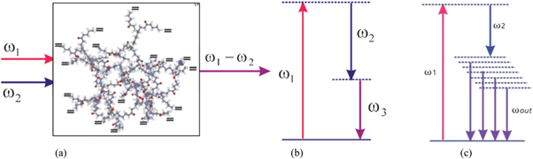
Figure 3. (a) Molecular structure of the 3th generation interaction geometry and dendrimer for different generation. (b) The energy level of different frequency generation. (c) Probable energy level results from chromophore and poling in dendrimer molecule. Reproduced from [33]. CC BY 3.0.
Download figure:
Standard image High-resolution imageIn the few years, some novel terahertz source techniques have been proposed. As examples, Bogue [42] summarized THz source techniques. An InAs/GaAs Quantum-Dot (QD) laser source [43] could be ultra-compact, tunable in normal temperature and setup its experiment with a QD based on photomixer with a compact, tunable double-wavelength QD laser in the dual-grating quasi-Littrow structure. A peak-power terahertz source has been constructed for ultra-fast electron diffraction with a working wavelength range of 50 μm to 200 μm [44]. Literature [45] proposed a device model composed of an electron source and a THz low-gain free electron laser oscillator. Paper [46] introduced a terahertz radiation source based on electron linear. In [47], based on optical comb, a referenced frequency source is presented to stabilize all kinds of THz source devices simultaneously. Optical combs could provide uniformly spaced CW light with significant precision and can be manufactured using a combination of a Mach–Zehnder modulator-based planar Comb generator and a greatly nonlinear dispersion shifted fiber. Figure 4 is a schematic diagram of the concept of locked phase multi-frequency terahertz source system [47].
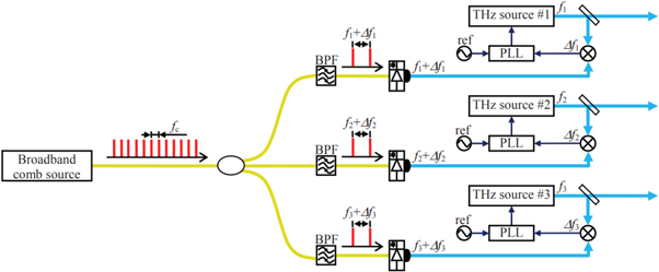
Figure 4. Schematic diagram of concept of locked phase multifrequency terahertz source system. © 2016 IEEE. Reprinted, with permission, from [47].
Download figure:
Standard image High-resolution image2.2. Component
All terahertz component, such as lenses, mirrors, and polarizers, manipulate specifically radiating. Traditionally, terahertz mirror is made of metal as silver, aluminum, gold, and copper. In order to get the maximum reflectance characteristics of the metal, the width on the metal coating could be at least as two skin depths at the incident beam with the frequency in [48]. Recently, some innovations in terahertz mirror technology including tunable mirror based on photonic crystals [49], hybrid mirrors [50], and semiconductors [51]. Terahertz lens is usually composed of plastic as poly-methylpentene or polyethylene. Nowadays, notable innovations have enabled the quick production of a huge lot of lenses [52], including 3D-printed diffraction lenses [53], Fresnel zone plates [54], variable-focal length lenses [55], plasmon resonance [56], and even paper terahertz lenses [57]. Polarizer is one of the important components of terahertz data transmission, imaging, and spectroscopy. Linear gate polarizers are easier to implement in the terahertz band than in the visible band [58]. Recent reconfigurable polarizers in reference [59] and carbon nanotube fiber polarizers as in reference [60] would been presented.
[49] gave properties of the ferrite materials in terahertz regime. Ferrite fully magnetized in an external static magnetic field can be seen as a gyromagnetic material, of which the permeability tensor can be derived from the Landau–Lifschitz equation in the following form:

The tensor elements μ and κ are given by


where ωex = γBex, ωm = γμ0 Ms , γ is the gyromagnetic ratio of 1.758 × 10¹¹ rad∕Ts, μ0 is the permeability in the vacuum, ω is the circular frequency of the incident THz wave, Bex is the external magnetic flux density, and Ms is the saturation magnetization of ferrite materials. In the measurement results from [49] the dielectric constant of LuBiIG is 4.85, the ferro-magnetic resonance linewidth is 2.8 to 5.1 Oe (1 Oe = 79.61 A∕m), and the saturation magnetization is 1560 G (1 G = 10−4 T), respectively.
In [54], grooved-dielectric FZP (Fresnel zone plate) of configurations and design procedure was proposed. Each lens is characterized by its aspect ratio ρ = F/D, where F is the lens focal length and D is the lens aperture diameter. Depending on the aspect ratio value the lens is defined as a high (ρ > 0.5) and low (ρ < 0.5) aspect ratio lens. The refraction lens with a high aspect ratio is considered thin while that with a low aspect ratio is distincted as thick. Thus, the size and weight benefits of the diffraction FZP lens over an ordinary (refraction) lens should be more pronounced in the case of low aspect ratio. FZP lenses with moderately-high aspect ratio 0.75 < ρ < 1.25 are very popular in quasi-optics. Such FZP lenses are considerably thinner than the corresponding ordinary lenses.
Basically, the FZP lens consists of so called full-wave zones with a radius bw calculated by [54].

where w = 1, 2,..., W is a current integer and W is the number of full-wave zones in the FZP. The full-wave zones are equiphase because the phase from one to another full- wave zone is altered by 2π.
All full-wave Fresnel zone in the FZP lens is divided in p = 2, 4, 8,... subzones. In each subzone s, the phase is changed by 2π/p relative to the phase in the neighboring subzone. The outer radius bs of s-th subzone is given by

where s = 1, 2,.., S, s = wp, and S = Wp.
2.3. Detector
Terahertz detectors can measure terahertz radiation at reception and play an important role in a lot of fields, including biology, astrophysics, imaging, explosive and chemical detection, astronomical applications, etc [61]. In 2010, Sizov et al [62] proposed various kinds of terahertz radiation detectors with heterodyne detectors [63] and fundamental direct detectors [64], two-photon detectors [65], Schottky barrier diodes [66], field-effect transistor detectors [67], and thermal detectors [68].
In 2008, Hesler et al [69] proposeed the testing and design of a wideband quasi-optical terahertz Schottky diode detector, which can be utilized as a set of waveguide detectors for providing reference points at the same location of the source beam. In 2018, Ikamas et al [70, 71] proposed a wide-band butterfly antenna coupled terahertz detector on 90 nm silicon CMOS FET for the identification of free space terahertz radiation. The detector could be enhanced by an internal design circuit according to physical model, and the terahertz detection was over 2 THz. The optical response rate is 45 mA W−1 (or 220 V W−1) [71].
2.4. System
The wide applications of terahertz radiation could be divided into four main categories: imaging, sensing, communication, and spectroscopy [72, 73], but also in preventive healthcare, quality control, non-destructive assessment, and surgery [74].
[25, 75] summarized the different application areas of terahertz technology, especially for food commodity safety and quality control. The table shows the potential of terahertz technology in the field of water detection and food, and discusses all kinds of other aspects, including foreign body identification, pesticide and antibiotic residue detection, edible oil characterization, and GM crop identification. For example, in the food industry, it is important to identify undesirable and potentially unhealthy organisms in food [4]. Most notable applications of terahertz radiation are entirely due to its large intrinsic properties and the unique fingerprint characteristics of biological tissues at certain frequency in the terahertz electromagnetic region. The harmful residues and antibiotics or the other agricultural productions in food are identified because of the different absorption properties of chemicals in the terahertz region. Regarding the penetration ability of terahertz radiation to fabrics, foams and plastics, it provides an effective technique for foreign matter detection in food quality control [25]. Though the notable absorption of terahertz radiation in water could not be acceptable in some applications, it is an advantage to explore different applications in humidity measurement as contamination detecting with the low-moisture productions, moisture quantification for fresh food. Due to the benefits of being non-invasive, non-destructive, and non-ionizing, terahertz technology has been described as an alternative method to sense water safety control or food and contamination detection. This terahertz system can be used in either transmission or reflection settings [75].
3. Detection methods
The field of terahertz technology has rapidly changed in the past years. The study work on THz technology has notably improved in the many novel technologies as terahertz time-domain spectroscopy, terahertz imaging, and THz radiation. The techniques have widely been researched and used in different fields.
3.1. THz Time-domain spectroscopy
The terahertz TDS could be set in three modes, including transmit, receive, and attenuated total reflection (ATR). Compared with reflection and transmission modes, ATR terahertz TDS is greatly suitable and sensitive for the measurement of high moisture samples [25, 76]. TDS system possesses the potential to directly obtain measurements of field phase information and amplitude information as a function of time through scanning the transient field of terahertz pulses. The terahertz frequency range could be accessed by using a Fourier transform to the time-domain data.
Daniel Richard Grischkowsky et al [77] used the method of time-domain spectroscopy to measure the far-infrared absorption and dispersion from 0.2 to 2 THz of the crystalline dielectrics sapphire and quartz, fused silica, and the semiconductors silicon, gallium arsenide, and germanium. As an effective method to identify spectral information of materials in the terahertz field utilizing ultrafast laser beam technology, terahertz TDS possesses a high signal-to-noise ratio of up to 120 (@peak Max) in time-domain data as to a wider frequency range and is applied in determining properties and profound structural changes of materials (or components) [78–80]. In 2018, Qu et al [81, 82] detected molecular classification and associated imprinting peaks for three plant growth regulators as 2, 4-dichlorophenoxyacetic acid, indole-3-acetic acid, and cyfluuron. In 2014, Baek et al [83] showed the feasibility of melamine classification in food and gave characteristic absorption peaks of melamine at 2 terahertz, 2.26 terahertz, and 2.6 terahertz respectively. In 2017, Zhang et al [84] quantified the percentage contribution of intramolecular vibrations to the normal mode by the molecular representation of sugar molecules by THz vibrational spectroscopy. In 2016, Cheon et al [85] reported terahertz molecular resonance imprints of deoxyribonucleic acid (DNA) methylation in cancer DNA with features that could identify different types of cancer cells. In 2018, Mieloszyk et al [86] tested different contaminants as gypsum, oil, and water, using glass-fiber reinforced composites and giave slower wave propagation in contaminated areas.
3.2. Radiation
THz radiation could refer to the region of electromagnetic radiation in the frequency range between 0.1 terahertz and 10 terahertz and between infrared and millimeter wave. The resulting terahertz rays have wide application prospects in imaging, environmental detection, communication, and medical diagnosis. Nevertheless, in the frequency range of THz radiation, THz wave transmission would suffer from slight group velocity dispersion and attenuation as to water molecules in the atmosphere [87]. Fitch & Osiande [12] presented the possibility of terahertz communication due to higher transmission rates and greater bandwidth, even in low source efficiency of terahertz radiation in the field of communications and the presence of strong atmospheric absorption.
3.3. Imaging
THz imaging is an important and prosperous non-destructive assessment technology for safety inspection, quality control [88–93], and fantastical applications as counting the number of almond bars using terahertz image detection techniques. A notable advantage of THz in the image process field is that THz radiation possesses the unique ability to penetrate common package materials, and may therefore give spectral information about the material inside.
In 2018, Yildirim et al [94] presented an active THz imaging automated biosecurity accessing and tracking gate system composed of terahertz imaging or scanning, autonomous conversion, and x-ray modules that are capabilities of detecting hidden objects on the human beings body. In 2018, Momivama et al [89] built a swept-source optical coherence tomography system working at frequencies from 600 GHz to 665 GHz, which could be utilized in quality control. In 2018, Ryu et al [95] proposed a compact portable terahertz imaging system based on a single-mode Fabry–Perot laser diode that is low in cost and simple in structure. In 2017, Stübling et al [96] presented a terahertz tomographic imaging system with a 3-D scanner, which can allow reflection of terahertz tomographic images of samples with unlimited surface shapes by taking a receiver and transmitter on a robotic arm and are applied in researching a different non-planar object, including mummies, biological specimens, cultural heritage, and made parts industrially.
3.4. Building materials
Employ THz radiation for non-destructive evaluation of materials and system interrogation is shown in [6]. Utilize these systems for some applications: (1) High-speed and high-field materials characterization; (2) Layer measurements; (3) Non-contact conductivity measurements. Moreover, the systems can be expected applications, such as, (1) Real-time, in situ conductivity and microstructure characterization for process monitoring of advanced and additively manufactured materials; Characterization of materials through rotational and vibrational spectra to verify microstructure; Examination of organic fuel pellets using THz computed tomography to help improve the packing density of material; (2) Measure layer and oxidation growth in situ in TREAT or other challenging environments; Monitor electrical conductivity of fragile samples using a non-contacting probe; Characterize materials used in nuclear applications, such as defect detection in Zr cladding; (3) Field deploying a ruggedized THz spectroscopy system for material identification; Characterizing and validating the next generation of armor materials; Testing of next-generation (beyond 5G) wireless systems and components; Integrated circuit interrogation through side channel emission analysis and direct conductivity measurements; Code injection and encryption using high-field THz pulses.
For the reader's convenience, we summarize the application of THz building materials in table 1.
Table 1. Application of THz in building materials.
| Material | Function | References | Note |
|---|---|---|---|
| Foam Polymer & Plastic Materials | Densities, Defects, & additives. | [97–103] | Terahertz techniques are helpful for superstructures [97], properties of dielectric material [104], voids [98, 99, 105], defects [98, 100, 101], inclusions [98, 106], material aging processes [107], and glass transition [108]. In addition, the wavelength of terahertz radiation is suitable to the additive or filler [98, 104] and the foam pore size [109, 110]. |
| Corrosion & Adhesion | [97, 111–113] | ||
| Clay & Ceramics | Control the porosity of ceramics | [110] | Terahertz waves are fit for ceramic analysis and can provide looking up the construction of opaque ceramic material. |
| Defects & Underlying Structure. | [114, 115] | ||
| Woods | Wood Defects & Density | [114, 116–118] | Detecting moisture and invisible flaws in wood (such as knots, rings, fungal decay, and termite damage) [114, 116, 117, 119–122]. |
| Water Absorption | [114, 119, 120] | ||
| Paints | Wet-Dry Conversion & Chemical Constitute. | [119, 123–125] | As for noncontact non-destructive test is terahertz wave detection, which is given to test film thickness and coating [123, 126], evaluate multilayer coatings [111, 123, 127], plot thickness distributions [123], detect inhomogeneity and coating layer defects [116, 123], monitor dry-wet conversion [123], and determine concentration or the chemical composition [128]. |
| Thickness & Defect. | [123, 125, 129, 130] | ||
| Composite Materials | Detect fiber orientation and content. | [98, 100, 104, 131] | THz technique shows notable potential for surface and interior examination of various composites, including wood-plastic composites [120], carbon fiber composites [100, 132], polyethylene fiber composites [133], polymer nanocomposites [134, 135], and glass fiber composites [136]. |
| Examining flaws. | [132, 137] | ||
| Glass | Refractive index and absorption of quartz and silica samples. | [138] | Studies on the refractive indices and absorption spectra of glass and glass-consolidated materials in the terahertz field are shown [75, 136]. |
| The ratio of preferred oriented glass fiber and fiber orientation. | [136, 139] | ||
| Brick, Concrete, Cement, Stone & Sand | The attenuation coefficients of broadly utilized building material. | [118,140] | THz waves are used to the study of the internal constructive concrete. |
| Concrete inner cracks or external flaws. | [114, 141, 142] | ||
| Assessing the water content of harden cement slurries. | [143–146] | ||
| Asbestos & Rock Wool | Analyse the existence of asbestos | [118] | It is not fortunate that long-term suffer in air asbestos fibers is not security to human beings and can lead to related asbestos diseases. |
| Detect corrosion in the pipe | [147] |
4. THz material research
4.1. THz waveguide material
Wang et al [30] review comprehensively introduces the latest developments in the field of terahertz waveguides, and prospects for its future applications. The dielectric fringe based terahertz waveguide proposed by Mahankali et al [9] is planned for 3 teraherrtz and constructed adapting high-density polyethylene, graphene, aluminum gallium arsenide, and gallium arsenide. Anatoly et al [148] investigated the properties of novel porous materials made from nanostructured aluminum hydroxide (NAO) in the terahertz range. They also discussed the terahertz TDS detection results of the adsorbed molecular layer on the NAO surface.
Gao et al [149] discussed the concept of all-silicon components based on their recently presented effective dielectric cladding dielectric waveguide. Yang et al [150] introduced the application of polymer-ceramic nanocomposites in the fabricating wafer-level terahertz flat circuits. Thin ribbon dielectric waveguides within 50 ∼ 60 μm made of BaTiO3 composites are adapted to fabricate terahertz circuits and ribbon waveguides. Permittivity is slightly frequency dependent. It decreases with increasing frequency. For different volume loads, the loss angle tangent of the material is tested to be lower than 0.05. It depends very much on the nature of the polymer material.
4.1.1. THz hollow metal waveguide.
Based on Drude model, the complex dielectric constant of THz band metal ε can be expressed as [151, 152]:

where, εr is the real part of the complex permittivity; εi is the imaginary part. There are:


where ωP is the plasma oscillation frequency.
Hollow metal waveguides use total internal reflection mechanism to guide THz wave. In 1999, McGowan and Gallot's team [153] successfully coupled THz waves of 0.8 ∼ 3.5 THz into a stainless steel circular metal waveguide with a diameter of 240 μm and a length of 24 mm, and its total absorption coefficient was less than 0.7 cm−1. In 2000, Gallot et al [154] continued their research on THz circular and rectangular metal waveguides, in which the circular waveguide size is still 240 μm in diameter and 24 mm in length, and the rectangular waveguide size is 25 mm in length and the cross section is 125 μm × 250 μm, and the material is still stainless steel.
In 2007, Lu et al [155] from Zhengzhou University calculated the metal-coated waveguide with metal coating on the inner wall of plastic or glass tube. Harrington et al [156] reported fabrication of flexed empty polycarbonate waveguide with internal copper coatings for transmitting broadband terahertz with ordinary liquid phase chemistry technology. It is found that the loss of the optimal waveguide is less than 4 dB m−1, and the single mode of the waveguide with smaller aperture can be preserved.
Zhang et al [157] fabricated dielectric metal film waveguides at microwave G band and 4.3 THz by plating metal film and dielectric film inside polycarbonate tube in 2019, and experimentally measured that waveguide loss in G band increases with the increase of dielectric film. In 2018, Seifert et al [158] proposed an all optical free contact method with large sample handling capacity that allowed to extract the spin current relaxation length and the spin Hall Angle.
After nearly 20 years of development, it can be seen that the loss of THz hollow metal waveguide has increased from 0.7 cm-1 to 0.025 cm-1, and the performance improvement is very obvious.
4.1.2. THz parallel plate waveguide
In 2001, Mendis et al [159] proposed THz parallel flat waveguide. They also glued two thin copper sheets together to produce a flexible parallel flat waveguide [160]. The 0.22ps THz pulse was widened to 0.33ps after passing through a 250mm waveguide, and its amplitude was attenuated 10 times.
In 2007, Mendis constructed a kind of dielectric-filled Metallic parallel-plate Waveguides (DF-PPWGs) [161] and found that although the absorption of high resistance silicon is smaller, compared with that of polyethylene, DF-PPWGs filled with high resistance silicon showed high transmission loss. Therefore, the key to realize low loss transmission in parallel planar waveguides is to use dielectric fillers with low absorption and refractive index.
In 2008, Cooke et al [162] realized the modulation of THz pulses by filling silicon with a transparent conductive Oxide film (Oxide is Tin fluoride Oxide, fluorine Oxide, FTO) in a parallel flat waveguide. There was not time delay between the air-filled waveguide and the confocal lens position, and the transmitted pulse keeps short with small reshaping. When an FTO-coated silicon plate of length L was inserted into a filled air copper waveguide, the pulses remained little and shifted Δt = L(nSi − 1)/c, denoting that the transmitted pulses remained single mode and propagated with only a little number of group velocity dispersion, and the group index was near to the bulk silicon.
It can be known that the group velocity dispersion of THz parallel plate waveguide is very small, but the loss has no obvious advantage compared with THz hollow metal waveguide. At the same time, it can also be found that people have realized THz wave modulation by filling medium in THz parallel plate waveguide, instead of simply studying its guided wave properties.
4.1.3. THz wire waveguide
In the field of THz wave transmission technology, wire waveguide is an important waveguide, which has the advantages of low dispersion and low loss. In 2004, Wang et al [163] proposed a bare-metal linear waveguide to solve the problem that THz wave cannot transmit over long distances, which has the advantages of low dispersion and low loss. In 2005, they [164] constructed a simple Y-type beam splitter on this basis.
In 2005, Jeon et al [165] carried out experimental and theoretical research on the propagation of terahertz wave on a single Cu wire, which shows THz pulse attenuation when copper wire is bent Δh in the experiment.
He et al [166] studied the transmission characteristics of THz wire waveguide in 2006, and analysed the influence of several common metal materials on the transmission performance.
THz wire waveguide possesses the advantages of simple structure, high flexibility, easy bending, low dispersion and low loss. However, as wire waveguide is a kind of bare structure, its anti-interference performance is not very good, so additional design is needed to compensate.
4.1.4. THz fiber optic medium
THz fibers are usually made of dielectric materials, especially polymer materials, because they have lower absorption losses and lower dispersion coefficients in the THz band. For example, polytetrafluoroethylene (PTFE, or Teflon), polymethyl methacrylate (PMMA), polyethylene (PE), polypropylene (PP) and cycloolefin copolymer (COC).
In 2000, Grischkowsky et al [167] studied the waveguide propagation characteristics of sub-picosecond THz pulses in single crystal sapphire fiber.
In 2006, Chen et al [168] studied THz fiber made of polyethylene. They used polyethylene fiber as the core of the fiber with high refractive index and directly used air as the cladding. They realized transmission of 0.3 THz wave in 200 μm diameter polyethylene fiber with loss as low as 0.01 cm−1. THz dielectric fiber, different from the traditional quartz fiber, the performance of polyethylene fiber is very outstanding, its transmission of THz wave, loss can be as low as 0.01 cm−1.
4.1.5. THz dielectric tube waveguide
Dielectric tube waveguide is composed of dielectric tube and air core in the middle of tube. It has simple structure and low transmission loss. Its working mechanism is anti-resonance guiding mechanism. When operating at the antiresonance frequency, THz waves are fully reflected by the inner wall of the dielectric tube and thus transmitted through the inner air core.
In 2009, Lai et al [169] studied the THz dielectric tube waveguide made of PTFE. In 2010, Lu et al [170] carried out an experimental research on the bending loss of terahertz PTFE tube waveguide, and studied the influence of frequency, polarization, core diameter, cladding thickness and cladding material on the bending loss of the waveguide. The results show that the lower waveguide loss is due to the stronger mode constraint and the lower bending loss.
In 2015, Bao et al [171] measured three sizes of polymethyl methacrylate (PMMA) dielectric tube waveguides with hollow kernel diameter of 4 mm, and cladding thickness of 1.29 mm, 1.97 mm and 2.95 mm, respectively. The loss was measured in the range of 0.3 to 1 THz in the range of 0.05 to 0.5 cm−1.
In THz dielectric tube waveguide, PTFE performs extremely well, its coupling efficiency can reach 80%, the lowest loss is far less than other materials dielectric tube waveguide, also far better than other types of THz waveguide, and has a broad application prospect.
4.1.6. THz photonic crystal
In 1987, Yablonovitch [172] proposed the concept of Photonic Crystals (PCs) while studying how to suppress spontaneous radiation in solid physics and electronics. Almost at the same time, John [173] also proposed the concept of photonic crystal when discussing the photon local problem in disordered medium superlattices. It is thus possible to introduce concepts related to solid state physics into such superlattice problems, introducing the concept of band gaps. On this basis, Yariv [174] put forward the theory of photonic crystal waveguide in 1999.
Referring to Mr Huang solid State physics [175], the starting point of tight binding approximation is that when an electron is near an atom, it will be mainly affected by the action of the atomic field, and the action of other atomic fields is regarded as the perturbation, so obtaining the correlation between the crystal energy band and the atomic energy level of the electron. The main method is Linear Combination of Atomic Orbital Method (LCAO).
In terms of actual processing technology, the preparation of one-dimensional photonic crystal is relatively simple, but because its periodic structure is one-dimensional, relatively complex defect mode cannot be constructed, so it can realize not too many functions. The defect modes of 3D photonic crystal can be constructed are very rich, so many functions can be realized, but the preparation process is relatively complex and the cost is high. However, two-dimensional photonic crystals have both advantages, so the actual research is mainly focused on two-dimensional photonic crystals.
- (i)THz photonic crystal waveguideIn 2006, Zhang et al [176] proposed a silica-based 2-D photonic crystal waveguide and numerically simulated the applicability of... THz multi-mode interference effect and self-imaging principle in 2-D Si photonic crystal waveguide. In 2009, Ponseca et al [177] analysed the transmission properties of lens conduit, Cytop planar photonic crystal waveguide and hollow micro-structured PMMA fiber in THz region. In 2012, Kitagawa et al [178] systematically studied the band structure of two-dimensional photonic crystal made of dielectric with a low dielectric constant, and proposed a flat waveguide of THz low-dielectric two-dimensional photonic crystal sandwiched between two parallel metal plates.In 2015, Tsuruda et al [179] proposed a photonic crystal waveguide based on high resistance silicon plate (resistivity of 20 kΩ/cm) in order to develop a photonic crystal waveguide with extremely low loss. In 2021, Si et al [180] designed a band-stop filter based on two-dimensional silicon photonic crystal waveguide and AAH (Aubry-Andr-Harper) resonator. Its stopband centre wavelength is 1668.3 μm, its stopband attenuation is 25.2 dB, and the passband insertion loss is 0.2 dB. With a high Q value of 1.5 × 10⁴, it is very convenient to build integrated optical path.THz photonic crystal waveguide has natural advantages in integrated optical path due to its extremely low loss and high Q value when conducting waves at large angles. Due to the suitability of semiconductor technology in THz band and the consideration of integrated optical path and integrated circuit, most THz photonic crystal waveguides are currently developed based on semiconductor materials [181].
- (ii)THz photonic crystal fiber
Photonic crystal fibers are separated into Total Internal Reflection (TIR) type and Photonic Bandgap (PBG) type based on different light guiding mechanisms.
In 1996, Knight [182] reported at fiber-Optic Communications Conference that the first photonic crystal fiber was based not on photonic crystal band gap theory, but on total internal reflection theory like conventional fibers. PBG type photonic crystal fibers were fabricated by Knight et al in 1999 and published in Science [183].
THz band photonic crystal fiber did not appear until 2004 [184, 185]. In this year, Goto et al [184] from Japan produced low-loss THz photonic crystal fiber by using PTFE. Later, photonic crystal fibers with various structures were developed. In 2014, Li et al [186] developed a new triangulated lattice THz photonic crystal fiber with high birefringence and low dispersion over a wide spectral range. By tune-up the structural parameter of the photonic crystal fiber, up to 10-3 birefringence can be obtained in the frequency range from 0.1 terahertz to 5 terahertz. In addition, the group velocity dispersion curve is close to zero and flat in the frequency range. So, it is adapted to transmit broadband terahertz pulse that remain polarized. Other photonic crystal fibers with various shapes, such as square [187] and hexagon [188, 189], have also attracted great attention.
The research on the working mode of photonic crystal fiber has also attracted great attention. In 2012, Chen et al [190] designed a new type of THz single-mode single-polarization photonic crystal fiber, which introduced asymmetric rectangular micro-hole array in its core region. In 2013, Han et al [191] carried out a numerical demonstration of 2× 6Gb/s mode multiplexing division transmission of 70 km long double mode photonic crystal fiber by using LP01 and LP11 acting as the mode converter between two orthogonal modes, and the mode crossing can be basically ignored and the power loss is less than 1.86dB. It reveals the possibility of combining mode multiplexing division and photonic crystal fiber technology to achieve large capacity transmission.
The best material of THz photonic crystal fiber and dielectric fiber is PTFE, and the dispersion and loss characteristics of THz photonic crystal fiber are further improved by introducing the photonic crystal structure into the fiber. There are also many other studies on THz photonic crystal fiber, such as THz ultra-wideband photonic crystal fiber [192, 193], THz photonic crystal coupling mode [194] and THz photonic crystal fiber preparation process [195, 196]. Literature [193] operation begins with two types of KF, which transverse cross sections are given.
4.1.7. THz isoplasmon waveguides with metal surfaces
The study of Surface Plasmon Polaritons (SPPs) began when Wood et al [197] observed an abnormal absorption peak after irradiating a grating with light in 1902, which is called the Wood anomaly. It was not until 1941 that Fano explained the anomaly from the electromagnetic wave mode of the metal-air interface [198]. In 1956, Pines was the first to theoretically explain wood anomalies through a model of collective free electron oscillations in metals, which he called 'Plasmons' [199]. In 1960, the concept of Surface Plasma resonance was proposed by Stern & Ferrell, which further promoted the theoretical research on Surface Plasma [200]. In 1968, Kretchmann & Otto respectively proposed the method of stimulating SPPs on metal [201, 202], so that comprehensive research on SPPs could be carried out widely. In 2003, Barnes 'Surface Plasmon Subwavelength Optics' summarized the development of this field and laid a solid foundation for it [203]. SPPs exist at the interface of various negative dielectric constant media and positive dielectric constant media, the most common is the metal-air interface [204–206]. When the electromagnetic wave is coupled to the metal surface, it will excite the collective oscillation of free electrons on the metal surface, forming a polarized wave. If the excited wave is a traveling wave propagating on the metal microstrip, it is called surface isoionization polariton. If they are standing waves, which exist on metal nanoparticles but cannot propagate, they are called local surface plasmons.
The plasma frequency of metal is generally in the ultraviolet band and has a high dielectric constant in THz band. Although metal can also realize surface plasmons (known as Sommerfeld-Zenneck waves [165, 207]) in THz band, the local ability is extremely weak. In 2004, Pendry et al [208] from Imperial College London realized SPPs in THz band by introducing sub-wavelength scale square hole array on metal Surface, which is called Spoof Surface Plasmon Polaritons. SSPPs). Pendry's team found that by diluting the concentration of free electrons on the metal surface, they increased the skin depth of electromagnetic waves on the metal surface, triggering SSPPs-like patterns on the metal surface, called SSPPs. The dispersion relationship can be obtained by solving the Maxwell equation. For simplicity, Pendry assumes a square array of side d and a square cross section a × a for the hole in figure 5. In 2008, Williams et al [209] changed the square holes into grooves and made the THz band SSPPs structure.

Figure 5. The model system: a × a square hole made on a d × d grid is divided into the surface of an ideal conductor. From [208]. Reprinted with permission from AAAS.
Download figure:
Standard image High-resolution imageIn 2008, Fernandez-Dominguez et al [210] proposed a periodic metal linear waveguide. In this year, Fernandez-Dominguez et al [211] studied the propagation of tightly bound THz-SSPPs on spiral groove wires both theoretically and experimentally. The periodic structure of the wires can allow the formation of surface electromagnetic patterns with different azimuthal symmetry at wavelengths longer than the pitch. In 2009, Zhang et al [212] developed a subwavelength grating waveguide based on SSPPs, which consists of two parallel metal plates with periodic wavy inner boundaries to slow down the propagation speed of THz wave. In 2010, Gao et al [213] designed a structure consisting of a single row of metal wedges that periodically protrudes from the flat metal surface.
In 2013, Shen et al [214] presented the fabrication of ultra-thin metal gratings on ultra-thin flexible substrates, called Conformal Surface Plasmons (CSPs), realizing the two-dimensional structure of SSPPs. The team developed many functional devices based on this structure, such as SSPPs antenna [215], filter [216], second harmonic generator [217], etc.
In 2016, Liu et al [218] studied the dispersion characteristics of an ultra-thin metallic slotted SSPPs waveguide in THz band by applying the finite element method. They also studied the transmission characteristics of subwavelength planar SSPP waveguide ring resonator.
In 2016, Liu et al [219] presented and studied a THz electron source based on the effective generation of SSPPs mode in a double-corrugated metal waveguide. In 2017, Chowdhury et al [220] studied periodic fluted metallic THz waveguides filled with media. In 2018, Zhang et al [221] designed THz-SSPPs waveguide based on one-dimensional grating structure, and constructed S-bent waveguide, Y-type beam splitter and directional coupler on this basis. In 2018, Guo et al [222] proposed the realization of cotype SSPPs waveguide in THz band for the first time. In 2019, Jaiswal et al designed a bandpass filter based on a similar structure [223]. In 2020, Xu et al also designed a similar structure [224]. These studies are limited to numerical calculation in THz band, and experimental verification is carried out in microwave band. In 2021, Rahman et al [225] tested four samples of jet-deposited nickel layers on alumina layers by high-resolution THz time-domain spectroscopy. Once the correct spot is selected, the built-in motion screw is adjusted for maximum reflection, thus ensuring that the T-ray beam on the sample surface is incident vertically [225].
In a word, there are more and more researches on SSPPs, and various devices based on SSPPs have been developed, but most of them are limited to the microwave band. Although the research on THz band SSPPs waveguide is not rare, it is limited to theoretical and simulation work due to many practical reasons such as signal source and detector, and the experimental work is very rare, which is almost an unexplored direction and still has great potential.
4.1.8. THz waveguide based on novel two-dimensional materials
Graphene, as the most representative new two-dimensional material, has excellent performance in force, heat, light, electricity and other aspects, and has a good application prospect in biology, medicine, materials and other directions. In recent years, it has been payed for wide attention and has been studied in depth continuously [226–230].
Graphene is typically only 0.2 to 0.5 nm thick, which is lower than the thickness of metal films that can be processed with existing techniques. Graphene exhibits an extremely high carrier mobility of 20 000 cm2/(V·s) at normal atmospheric temperature (when electron density is 2×1011 cm−2) [231]. The light absorption of graphene is divided into two types: interband absorption and in band absorption [232]. In 2008, Hanson [233] proposed the THz Parallel Plate Waveguide (GPPWG) model for the first time. In 2011, Vakil & Engheta [234] used bias voltage to regulate the SPPs properties of graphene. In 2012, Yuan et al [235] designed a semiconductor-graphene cylindrical THz waveguide. In 2014, Wang et al [236] designed parallel and series couplers based on graphene SPPs waveguide. The dispersion curve of the graphene SPPs waveguide and the state transition of the coupler are able to be controlled by changing the bias voltage.
In 2018, Chen et al [237] proposed a novel Graphene /AlGaAs SPW structure combining Graphene Surface Plasmon Waveguides (GSPW) and nonlinear materials. It is used to generate terahertz wave difference frequency generation under near-IR pumping. In 2019, He et al [238] theoretically reported a novel graphene-based Hybrid Plasmonic Waveguide (Graphene-based Hybrid Plasmonic Waveguide) by integrating GaAs microtubes onto silica gasket supported by Graphene coating substrate. GHPW). In 2019, Zheng et al [239] also proposed a new TYPE of GHPW.
Compared with traditional materials, graphene exhibits superior characteristics such as stronger mode constraints and longer transmission distances while being workable with thinner thickness. It can be seen that graphene has broad prospects in the field of THz. At present, although the research on new 2D materials mainly focuses on the two directions of gold film and graphene, the research on other new 2D materials, such as WSe2 [240], WS2 [241, 242], MoS2 [243] and black phosphorus [244], is also continuous. In order to further illustrate that 660 nm is a good modulation effect as a pump light excitation sample, the throughput curve of WS2 film is calculated [240]. The thickness better than WS2 film is only 0.65 nm, and the transmittance of the film cannot be measured directly. Therefore, the result is calculated from the transmittance of substrate Si and WS2 Si samples. The unit of the terahertz absorber is given in figure 6 [243]. Figure 7 is a schematic representation of their presented plasmon sensing structure, where a single layer of BP is separated from the germanium prism by a TPX and crystalline quartz layer, and other TPX and crystalline layers are sequentially arranged between the BP and sensing medium layer [245].
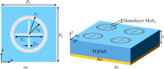
Figure 6. Presented absorber with MRC layer. (a) Top view. The geometric parameters: px = py = 60 μm, r1 = 20 μm, r2 = 16 μm, c2 = 2 μm, c1 = 30 μm. (b) The structure of the MRC array and the bottom gold layer are divided by a thin TOPAS dielectric layer with a thickness, h = 26 μm. Reprinted from [243], Copyright (2021), with permission from Elsevier.
Download figure:
Standard image High-resolution image
Figure 7. Schematic diagram on black phosphorus or waveguide plasmon structure. Reprinted from [245], Copyright (2021), with permission from Elsevier.
Download figure:
Standard image High-resolution image4.2. THz metamaterials
4.2.1. Research overview of THz metamaterials
Metamaterial, also known as new artificial electromagnetic media and metamaterial materials, is characterized by arranging artificial unit structures (artificial atoms) with subwavelength scale in periodic or aperiodic order, thus obtaining electromagnetic properties beyond the limits of natural materials. For example, negative refractive index, zero refractive index, ultra-high refractive index, high-frequency magnetic response, etc [246–249]. Since the 1990s, researches on the basic theory, functional devices and engineering applications of electromagnetic metamaterials have attracted extensive interest in physics, information and materials fields. Based on the electromagnetic parameters and their distribution that can be designed by metamaterials, researchers have developed a variety of new devices such as metamaterial cloths, lenses and antennas [250–255]. According to the field-local and field-enhancement characteristics of metamaterials (this effect is particularly significant in surface plasmon metamaterials) and the characteristics of sub-wavelength scale, novel metamaterials sensing and imaging devices are developed, which can effectively improve the sensitivity and imaging resolution of sensors [244, 256, 257]. With the introduction and implementation of digital coding and programmable metamaterials, the characterization and design of metamaterials are carried out in binary digital mode (i.e., the numbers 0 and 1), which promotes the integration of metamaterials and information technology and makes it possible for new system metamaterials imaging system and communication system [246].
The terahertz frequency region is intermediate between far-IR and microwave in the electromagnetic spectra and is generally defined as electromagnetic radiation of 0.1 ∼ 10THz [258]. With the rapid developing THz sources and detectors and the continuous development of terahertz functional devices, terahertz science and technology have made vigorous development in recent years. Terahertz technology has a good application prospect in material characterization, security inspection, biomedical imaging and communication, etc [259, 260]. In terms of imaging, compared with microwave and millimetre wave frequencies, the terahertz imager will have higher spatial resolution, and compared with optical imaging, terahertz radiation has better penetration, so more depth information can be obtained [261]. At the same time, terahertz imaging applications have been receiving a lot of attention because it is a non-ionizing radiation with better biosecurity. Terahertz metamaterials and metamaterials have broad application prospects in terahertz imaging systems due to their advantages of subwavelength unit scale and flexible control of electromagnetic wave amplitude, phase and polarization characteristics [262, 263].
In the 1990s, Sir John proposed the method of equivalent media parameters to construct the negative permittivity and negative permeability of low frequencies [264, 265], and the team of Prof. Smith verified the experiment in microwave frequency [266]. Since then, electromagnetic metamaterials have been the hot topic to research for more than 20 years. With the application of micro-Nano processing technology, metamaterials in terahertz, infrared and visible wavelengths can also be realized in the laboratory [267–269]. In particular, terahertz magnetic metamaterials break through the limitations of natural materials and obtain magnetic responses at high frequencies [267]. Terahertz metamaterials can also be used to obtain negative or ultra-high refractive indices. At the same time, researchers have developed a variety of new terahertz metamaterial devices, including cloaks, absorbers, modulators and optical switches, to regulate the propagation properties of terahertz waves [270–272].
Electromagnetic metasurface, as a kind of two-dimensional metamaterial, has attracted extensive research interest. Compared with 3D metamaterials, metamaterials have deep subwavelength thickness, and their manipulation of electromagnetic waves does not depend on phase accumulation in space, but on the phase gradient (discontinuous distribution) between adjacent elements to realize the manipulation of electromagnetic wave front, amplitude, phase and polarization [273]. Therefore, adopting the metasurface scheme is beneficial to the design of ultra-light, ultra-thin and easily conformed terahertz devices, such as metasurface abnormal reflection/refraction devices, polarization converters and low scattering devices [179–276]. Through the combination of metasurface and a pair of orthogonal gratings, abnormal deflection and efficient polarization conversion of transmitted terahertz linearly polarized waves can be realized [276]. Therefore, terahertz metasurface devices can achieve flexible manipulation of terahertz beam and have the advantages of light weight and easy conformal.
4.2.2. Tuneable & reconfigurable THz metamaterials
Commonly used materials include superconducting materials, graphene, liquid crystal, phase change materials, titanate and magnetic materials, etc [263, 277].
Chen et al [278] designed terahertz SRR metamaterial on YBCO (YBa2Cu3O7−δ , δ = 0.05) superconducting film with a thickness of 180nm, whose terahertz resonant frequency and transmission properties are adjustable with temperature. The metamaterial device covers a monolayer of graphene on the surface of a zero-refractive index metamaterial and realizes the adjustable Goos-Hänchen effect by electrically adjusting the Fermi energy levels of graphene [279]. For example, LC1852 has a THz normal and abnormal refractive index of 1.56 and 1.89 respectively, so it has potential applications in THz adjustable metamaterials, THz phase shifters and THz beam scanning devices [280]. The liquid crystal/metamaterial adjustable absorber structure consists of a resonant unit, a liquid crystal layer and a metal backplane layer [281]. The problems encountered in the design of LC-based terahertz components are systematically solved [282].
The conductivity of epitaxial VO2 film can reach 105 S m−1, so the complex dielectric constant needs to be considered [283]. VO2 has been widely used in tuneable metamaterials [284]. Zhu et al [285] gives a schematic diagram of the VO2/metamaterial filter. Hillman et al [286] designed a broadband terahertz phase shifter using VO2, which achieved a phase shift of more than 300° in the frequency range of 220 ∼ 250GHz, which could be applied to terahertz beam manipulation including beam scanning. Metamaterials and devices based on dielectric materials (such as titanate) are also adjustable with temperature [287].
Magnetic materials are also widely used in tuneable metamaterials. Bi et al [288] designed a magnetic metamaterial unit using Mn-Zn microwave ferrite material, and realized a thermally adjustable negative refractive index by recombination with metal wire element. In addition, magnetically tuneable wideband microwave filters can be realized by using ferrite-based metamaterials [289]. Liu et al [290] shows that when the intensity of magnetic field bias is 194mT, the modulation depth of terahertz transmission amplitude can reach 34%.
Reconfigurable metamaterials generally refer to the reconstruction or adjustment of metamaterials' properties through the reconstruction of their geometric structures. Common approaches to reconfigurable metamaterials include micro-electro-mechanical systems (MEMS) techniques and deformation techniques such as thermal and stress-induced deformation [291, 292]. It is also a common method in MEMS technology to change the height of the cantilever beam by driving voltage, and then adjust the geometric parameters and resonant frequency of metamaterial unit [293]. Metamaterials composed of materials with different thermal conductivity are usually bent by lifting and cooling, or substrates with good ductility are stretched to change metamaterials' geometric parameters [292].
In addition, active metamaterials can be constructed by introducing active components or functional materials, such as diodes, semiconductor materials and graphene, into metamaterials [294, 295]. Active control of THz electromagnetic induced transparency is able to be realized by changing the electrical conductivity of Si by changing the optical pumping intensity [295]. By dealing with the intensity distribution of pump light, the pattern reconstruction of the metasurface can be realized [296]. The cell of EIT metamaterial composes of cut wires (CW) and two SRRs, in which the silicon island is located in the gap in figure 8(a) [295]. The metamaterial structure was made of a silicon wafer on sapphire consisting of an undoped silicon film 500 nm thick and a sapphire substrate 495 microns thick. As shown in figure 8(c), electro-optic time-resolved OPTP system is used for measurement. The tested amplitude transmission for the first as continuous wave only and second samples as SRR pair are only given in figure 8(d).
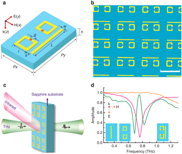
Figure 8. Design Experiment and tested transmission spectrum. (a) Schematic on the cell. The geometrical parameter: l = 29, L = 85, s = 7, h = 495, g = 5, w = 5, Py = 120 and Px = 80 μm. (b) Microscopic images of metamaterial produced. Scale bar, 100 μm. (c) Schematic diagram on the experiment for the measurement of EIT metamaterial by optical pump THz probe. (d) Tested amplitude transmission spectrum of unique continuous wave in pink, SRR pairs in orange, and the EIT metamaterial samples in olive. The inset in (d) shows the structuring geometry of the distinctive continuous wave, SRR pair, and the EIT metamaterial samples from left to right with polarizing diagrams. Reproduced from [295], with permission from Springer Nature.
Download figure:
Standard image High-resolution imageTuneable, reconfigurable, and active metamaterials enable metamaterials to function not in a fixed state, but in an excitable manner, allowing them to operate at adjustable frequencies or switch between different functions, allowing them to manipulate the transmission properties of electromagnetic waves with greater freedom.
4.2.3. THz digital coding with programmable metasurface
Prof. Cui presented the concepts of digitally coded metamaterials and field-programmable metamaterials [274]. Moreover, 1-bit, 2-bit and 3-bit digitally encoded metasurface can be got by selecting units of different sizes [297]. Single beam, double beam, multi-beam radiation and RCS reduction of terahertz wave can be obtained by optimizing the coding pattern.
The digital coding sequence is input into field programmable gate array, namely FPGA, and the bias voltage is controlled by FPGA to realize the real-time switching of the coding pattern of metamaterial array, to control the far-field radiation properties of metamaterial array [274]. Cong et al [298] designed a terahertz programmable metasurface scheme based on MEMS process.
As shown in figure 9(a), the authors think about special metasurfaces [274] consisting of binary numeric elements of '0' or '1'. Nevertheless, to achieve a wide band, they implement the binary element in figure 9(b) using a subwavelength square metal patch printed on the dielectric substrate. For example, on 010101... / 010101..., under a periodic coding sequence, the normal incident beam is mostly reflected by the metasurface to two symmetrical orientations, while in 010101... / 101010... / 01001... / 101010..., as given in figures 9(c) and (d).
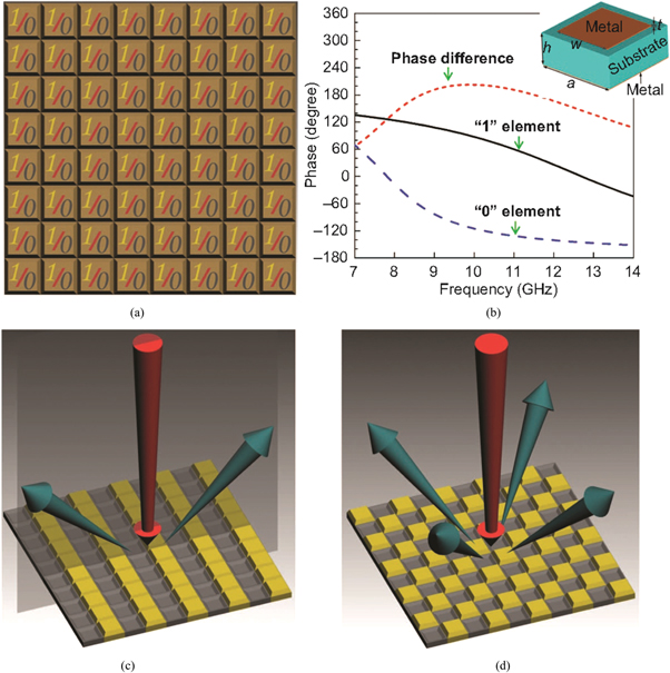
Figure 9. The surface of the 1-bit numeric element and the surface of the encoded element. (a) The surface of a 1-digit element consists of two kinds of parts: '0' & '1'. (b) Square metal patch cell for achieving '0' & '1' and According to phase response in the frequency field. (c, d) Two 1-bit periodic coding element surfaces, which determine beam scatter by design coding sequences of '0' & '1' parts: (c) 010101... / 010101..., and (d) 010101... / Reproduced from [274]. CC BY 4.0.
Download figure:
Standard image High-resolution imageMEMS-based MIM systems typically consist of structured metal resonators designed as suspended cantilevers that can be reconfigured by applying electrostatic forces, and continuous metal planes separated by dielectric spacers on the substrate [298].
Digital coding metamaterials with field programmable metamaterials metamaterials, also called information through super material description method and the design method of digital, implements the metamaterial with the integration of information technology, so metamaterials can be directly to digital information processing based on information, and to develop a new system of wireless communication system and the imaging system.
5. THz technology trends
5.1. Terahertz spectroscopy & imaging
Many research and industrial applications related to architecture require non-destructive, non-contact and spatially resolved research. Several methods are presented to meet the need, including terahertz waves, microwave radiation, x-rays, infrared wave, and neutron radiation, which cover different parts of the electromagnetic spectrum. To improve the reliability of the measured data, each method has its limitations and advantages that should be considered, particularly when integrated. The review adds two additional techniques, visual and ultrasound methods, which also are broadly utilized in the building and construction industries. For an example, terahertz waves have been integrated with ultrasound to boost comparison and resolution for imaging [299], and with confocal microscopy and electron to comprehend the relationship between the microscopic and macroscopic structures of material [98].
Terahertz waves have several disadvantages that are of extreme interest to manufacturers and research scholars, particularly in order to promote current application in industrial settings. The review highlights the most significant shown in figure 10.
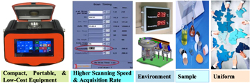
Figure 10. THz promoted current application in industrial settings.
Download figure:
Standard image High-resolution imageThese shortcomings can be promoted by utilizing different statistical analysis technology, decision trees, and neural networks, which are particularly helpful for samples with impure chemical properties. Such as building material. Other possible solution to promote the reliability of terahertz result is to propose the terahertz standard in the sample preparation, the measurement, and the system design.
5.2. Development trend of terahertz technology in material research
Although terahertz spectroscopy and imaging technology have preliminary potential in some uses in the constructing industry, it can be seen that there are still many areas to be studied in this field. Here, the paper will briefly give some problems related to the trend of construction and construction industry [300–302], which should be thought about in future.
5.2.1. Energy saving thermal insulation material
The major effect of the insulation layer could be to make inferior thermal transmittance and thermal conductivity, which mainly relates to the thickness of the materials and several other factors in detail by Jelle [302]. Nevertheless, terahertz spectroscopy is used to detect most of the properties, such as gas, material moisture content, and thickness, infrared transmittance, temperature dependence, and material densities. High power terahertz imaging is able to discover the structure of traditional insulating material, including the content of fibers or fillers and the orientation of fibers, which decide the mechanical and physical characters of the final materials and is able to controlling in the process. In addition, since terahertz wave is also able to detect gas, it is used to estimate the presence of expanded gases captured in units of conventional polymer foam after production.
As the energy consumption of buildings and construction fields accounts for an important proportion of the total energy consumption in the world, new thermal insulation materials are proposed to promote the energy efficiency of building. Compared with the conventional building envelope, the new thermal insulation material has the advantage of thinning or forming multi-layer structure, which also is fit for terahertz sensing. Currently, the aerogel is the most prosperous high-performance thermal insulation material [303], which has a high porosity, making it easy for terahertz wave to penetrate the material. Therefore, terahertz systems are adapted to regulate the producting procedure of aerogels. As an example, the unbound form alkoxide group in the silica aerogel network, the water content in the pores over drying, and the distributing large pores in the materials, which could not be ideal for an insulation purpose. Terahertz TDS is utilized to research the adsorption procedure of silica aerogels on molecular vapours such as ammonia, water, chloromethane, and others [304]. Furthermore, terahertz imaging is also able to be used to visualize hidden flaws, such as water intrusion, cracks, etc in building envelope made of gas insulation panel or modern vacuum. The panel is composed of an overt porous kernel of fumed silica, which is wrapped by some layers of metal polymer, and even so a little puncture will raise the thermal conductivity and allow water and air to invade [302]. Phase varying material, such as non-paraffin, organic paraffin, metal materials or salt hydrate, added in the form of microcapsule or planar or cylindrical element has shown notable latent as insulating materials [305]. These main functions are to vary from a solid state to a liquid state when they are heated and vice versa when they are cooled. As for normal cases, the variation happens in the temperature varying from 18 to 32 °C [300] and is able to easily determined by terahertz spectroscopy combined with cryogenic systems. Figure 11 shows the development trend of THz in four fields.

Figure 11. The development trend of THz.
Download figure:
Standard image High-resolution imageTHz development trend mainly includes the following four aspects according to THz metamaterials as shown in figure 12.

Figure 12. THz development trend according to THz metamaterials.
Download figure:
Standard image High-resolution image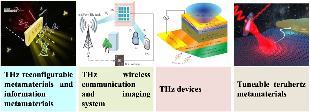
6. Conclusion
This paper reviews the application of terahertz spectroscopy in research and industry in recent years. At the same time, the key problems of the existing technology are summarized, and some new ways of application in the range of building material are proposed. Study and application require clearly that terahertz spectroscopy possesses broad prosperous for research scholars to discover material structure and engineers to control producing processes to improve material performance and durability. In addition, terahertz waves generate unique absorption spectra when passing through materials, which can be used to analyse moisture content, chemical composition, porosity, density, material thickness, food safety, material aging, etc Furthermore, the complementary imaging method can display surface and hidden internal flaws, inclusions and manufacture defects. The special properties can use terahertz spectroscopy to image a beneficial alternative or supplement to another sensing technologies with ultrasonic, infrared, microwave, or x-ray wave. Though the constructing industry is backward other industries in the application of terahertz technique and creative activities, there still are a lot of potential applications for the further study. It can be seen that when novel high-resolution, high-speed, and high-power sources make breakthrough progress, the potential of terahertz spectroscopy in building and material characterization will be significantly improved. Especially, in the future terahertz devices and terahertz materials, such as terahertz waveguide, terahertz metamaterials and metasurface are prosperous.
Data availability statement
The data cannot be made publicly available upon publication because they are not available in a format that is sufficiently accessible or reusable by other researchers. The data that support the findings of this study are available upon reasonable request from the authors.