


Abstract
The polarization beam splitter (PBS) is the essential optical component, which is widely used in various optical instruments. Its robustness against perturbation is very necessary to all-optical classical and quantum networks. Here, we report the design of topologically protected vector edge states (dual-polarization with transverse electric and transverse magnetic modes) and PBS based on all-dielectric topological valley photonic crystal slabs. The topologically protected vector edge states have been realized for the first time using germanium photonic crystal slab with silica substrate. Based on such edge states, the topologically protected PBS has been designed and its robust property has been demonstrated by exact numerical simulations. Our proposed PBS is expected to be widespread applications for photonic integrated circuits and quantum information processing.
Export citation and abstract BibTeX RIS

Original content from this work may be used under the terms of the Creative Commons Attribution 4.0 licence. Any further distribution of this work must maintain attribution to the author(s) and the title of the work, journal citation and DOI.
1. Introduction
The polarization beam splitter (PBS) is an essential device in traditional optics. It plays a significant role in classical [1] and quantum [2–5] optical experiments. For ultra-fast photonic integrated circuits, the PBS also has vital applications, such as all-optical information processing [6], optical encoding [7, 8], optical quantum gates [9–11], etc. Due to its importance, many scientists have designed various structures to realize the PBS, for example, wire waveguide coupler [12–14], photonic crystals (PhCs) [15–18], and multimode interference coupler [19, 20]. However, the footprints of these conventional PBSs are too large (from tens to hundreds of microns) to be integrated on a chip. Instead, other scientists have designed the ultra-small PBS by the inverse design method [21, 22], and its footprint may be several microns. But in fact, all these devices are vulnerable to perturbation. In this case, the efficiency and performance of the PBS are decreased. This limits the application of the PBS in complex environments. Therefore, it is important and necessary to design a robust PBS against some disturbances.
Recent developments in topological photonics have made it possible to complete this design. By introducing the topology into optics, some attractive phenomena have been observed [23–54]. At the microwave frequency, the photonic Chern insulator [42–45] shows lots of novel phenomena, including defect-immune and unidirectional propagating. Meanwhile, the all-dielectric topological PhCs [48–54] are easier to be fabricated on a chip without the need for external magnetic fields. Particularly, the topological valley photonic crystals (TVPCs) show high coupling efficiency and low transmission loss [49]. Therefore, the TVPC is a potential way to realize the topological integrated optical circuits. As far as we know, the all-dielectric TVPCs can support only one polarization mode, transverse electric (TE) [48, 50] or transverse magnetic (TM) [52, 53] mode. However, to design the PBS, topologically protected TE and TM modes should be presented at the same time. In fact, dual-polarization topological edge state has been studied by using metal materials in the previous work [55]. The use of metal materials limits the working frequency (around 6 GHz), and the same valleys for TE and TM modes cannot be used to realize the PBS in optical frequencies. How to design the topologically protected PBS is still a problem, although topological photonics has been intensively studied for more than 10 years.
In this work, we propose a scheme to construct the topologically protected vector edge states, supporting TE and TM modes, based on germanium (Ge) TVPCs [56] with silica substrate. The robust properties of these edge states are discussed. Furthermore, we design the PBS by such topological edge states. Especially, the proposed PBS possesses the properties of robustness against some disturbances. Actually, the PBS can be integrated into a compact photonic circuit, because the footprint of the integrated PBS is about 10 microns. It is expected that such a robust and compact PBS device has potential applications in future photonic integrated circuits.
2. Topologically protected vector edge states by all-dielectric TVPCs
We first consider the triangular lattices formed by the Ge triangular rod in the inset of figure 1(a). The lattice constant is a = 645 nm; the side of the Ge triangular rod is s = 500 nm; the thickness is d1 = 215 nm. The rods are surrounded by air at the top and bottom, and symmetric about the z = 0 plane. In figure 1(a), we plot the vector band structure of the system. Due to the C3v symmetry of the triangular lattices, the doubly-degenerate modes appear at K (K') point [57]. For the TE band and TM band, the same phenomena are discovered. At K and K' points, the gap between band 2 (1) and 3 (2) is closed for TE (TM) mode, and the double Dirac cone appears. For convenience in this paper, TM modes are marked in red, and TE in blue.
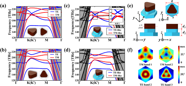
Figure 1. (a) The photonic band structure of the Ge rod with TE & TM double Dirac points. (b) The photonic band structure with a complete gap after 30° rotation of the rod. The band structure of the unit cell on SiO2 substrate with (c) no rotation and (d) 30° rotation. The TE-like and TM-like bands are marked as blue and red. The black points represent the leak modes above the light cone. (e) The unit cell consisted of Ge triangular rod and silica substrate, and its three views. (f) The eigenmodes of TM- (TE-) like band at the K point. Color: the absolute value of the electric (magnetic) field. Black arrows: power flux. Geometrical parameters in (b): a = 645 nm; s = 500 nm; d1 = 215 nm; d2 = 300 nm.
Download figure:
Standard image High-resolution imageAnd then, we rotate the triangular rod by 30°. Two Dirac points open and the complete bandgap appears, as indicated in figure 1(b). In figure 1(c), we introduce the 300 nm-thickness SiO2 substrate for the Ge rods. Due to the presence of substrate, the z-symmetry is broken. The TE and TM bands will couple with each other. Comparing to figure 1(a), it is found that the cross point of TE and TM bands opens, but the Dirac cones still exist. This phenomenon can be observed in figure 1(c). After the 30° rotation, two Dirac points also open, as shown in figure 1(d). To sum up, the substrate existing results in the coupling, and the 30° rotation results in the Dirac point opening. The geometrical parameters are labeled in figure 1(e): the lattice constant is a = 645 nm; the side of the Ge triangular rod is s = 500 nm; the thickness of Ge is d1 = 215 nm; the thickness of silica is d2 = 300 nm. In our design, the Ge film and half of the silica (d2/2 = 150 nm) should be etched away for minimizing the breaking of symmetry in the z-direction. In fact, the high index (more than 4) material (Ge) is indispensable for constructing the complete bandgap in figure 1(c), and only Ge rods can be used to design a practical device with the substrate.
With the rotation of the triangular rod, the complete bandgap can be observed around the wavelength of 1550 nm (193.41 THz) at K and K' points, as shown in figure 1(d). According to the C3v
symmetry group of the proposed lattice, the photonic bandgap at K and K' points is inequitable. Based on the
k·p
model [58, 59], the effective Hamiltonian around K/K' valley can be expressed as  , where vD
is the group velocity, and δ
k
=
k
-
k
K/K' is the displacement from the wave vector
k
to K/K' valley in the reciprocal space, σx
, σy
, and σz
are the Pauli matrices, m is effective mass [59]. It is known that the valley Chern number is CK/K' = ±sgn(m) = ±1/2. Interestingly in the topological complete bandgap, the valley Chern numbers of TE and TM band are opposite at the K point, i.e. CTM = −CTE. In general, the valley Chern number is in connection with the power flux of the eigenmodes. The power flux directions are clearly observed in figure 1(f). For the TE bandgap, the power flux is counterclockwise in band 2, and clockwise in band 3, which indicates the positive effective mass existing. It is in contrast to the TM bandgap, and its effective mass is negative. That is why the valley Chern numbers for TE and TM have the opposite signs.
, where vD
is the group velocity, and δ
k
=
k
-
k
K/K' is the displacement from the wave vector
k
to K/K' valley in the reciprocal space, σx
, σy
, and σz
are the Pauli matrices, m is effective mass [59]. It is known that the valley Chern number is CK/K' = ±sgn(m) = ±1/2. Interestingly in the topological complete bandgap, the valley Chern numbers of TE and TM band are opposite at the K point, i.e. CTM = −CTE. In general, the valley Chern number is in connection with the power flux of the eigenmodes. The power flux directions are clearly observed in figure 1(f). For the TE bandgap, the power flux is counterclockwise in band 2, and clockwise in band 3, which indicates the positive effective mass existing. It is in contrast to the TM bandgap, and its effective mass is negative. That is why the valley Chern numbers for TE and TM have the opposite signs.
Now, we consider a complex TVPC structure, which is made of upright (TVPC1) and inverted (TVPC2) triangles, as shown in figure 2(a). The edge state is constructed at the boundary of TVPC1 and TVPC2, which is marked in yellow. Furthermore, a supercell is taken (the inset in figure 2(b)) from the complex TVPC to analyze the properties of the edge states. Along the x-direction of the supercell, the lattice length is a = 645 nm, and periodic boundary condition is applied. In the y-direction, the length is about 10 μm (20 layers). By calculating the eigenmode of the supercell with the wave vector k x (from 0 to π/a), we get the corresponding band structure, as plotted in figure 2(b). The TE-like (TM-like) bands are marked as red (blue) lines. Importantly, the TE (TM) edge state has a positive (negative) group velocity at K valley, because of CTE = −CTM. That is to say, the sources with different chirality can excite the edge states with the same directions of propagation for the TE and TM modes.
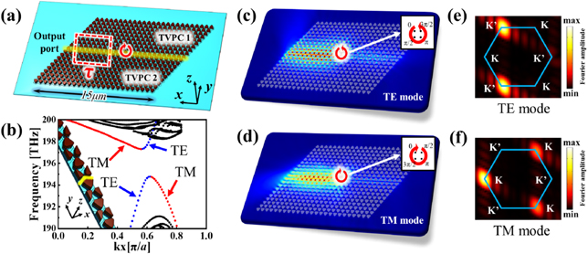
Figure 2. (a) Two types of TVPCs. A chiral light source is placed at the boundary. The red dashed rectangle: Fourier integral region. The yellow line: the boundary. (b) The topological vector edge states, including TE (blue) and TM (red) edge states. The inset: the supercell. The steady-state distributions of the absolute value of the electric field of (c) the TE mode and (d) TM mode. The insets: the TE (TM) light source consisted of four magnetic (electric) dipoles. (e) and (f) Fourier spectrum, which is obtained by Fourier transforming Hz or Ez distribution inside the rectangle delineated by the red dashed lines in (a); the hexagonal first Brillouin zone is indicated by the blue solid lines.
Download figure:
Standard image High-resolution imageMoreover, the gap of the edge states is opened as shown in figure 2(b). The TE and TM edge states couple to each other. That is because the silica substrate breaks the symmetry in the z-direction. In fact, lots of interesting phenomena happen if the edge states open the gap, such as the high-order photonic topological insulator [60, 61]. The dual-polarization corner state may be found at the frequency in the gap. This potential research direction might be got more attention.
And then, we study the method to excite the vector edge state. In the TVPCs, it is well known that the chiral source can excite the unidirectional topological edge state. For our model, different chiral sources are needed to excite the same direction of propagation of TE and TM modes at λ = 1550 nm. The source is placed at the boundary between TVPC 1 and TVPC 2, as shown in figure 2(a). Four magnetic (electric) dipoles in the z-direction are used to excite the TE (TM) topological edge state. Their phases are set as 0, π/2, π, and 3π/2 with counterclockwise (TE) and clockwise (TM) chirality, as shown in figures 2(c) and (d). K' and K valleys are respectively excited for TE and TM modes, and the edge states propagate to the left along the boundary.
To further study the vector edge state, we choose a Fourier integral region area
τ
in figure 2(a) for disclosing the propagating property in the momentum space (
k
-space) [62]. The size of rectangle
τ
is taken as 6 cells × 6 cells. For the TE mode, the Fourier transform formula is  . For the TM mode, the Fourier transform formula is
  . The results of fTE and fTM are plotted in figures 2(e) and (f), respectively. We find that the K' (K) valley is highlighted in the TE (TM) mode. It definitely indicates that the left-propagating edge states of the TE and the TM modes are locked in different valleys (K' and K). This interesting phenomenon can be used for polarization beam splitting based on different valleys.
Next, we note that the designed vector edge state possesses the topological property against some disturbances. In order to demonstrate topological robust transport of the vector valley edge states, we construct the Z-type, and Ω-type interfaces in figures 3(a) and (b). The boundaries (yellow) are bent as two or three 60° sharp corners. The numerical simulations are carried out at the wavelength λ = 1550 nm. With the chiral light sources exciting, the robust properties of the unidirectional transport are revealed, as shown in figures 3(c)–(f). In fact, the same bends are non-negligible for the traditional optical waveguide, because the bends can be usually considered as scatterers.
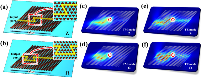
Figure 3. The topological vector edge states with (a) Z-type, and (b) Ω-type topological interfaces. The steady-state distributions of the absolute value of the electric field of (c) the TM mode with Z-type interface; (d) the TM mode with Ω-type interface; (e) the TE mode with Z-type interface; (f) the TE mode with Ω-type interface.
Download figure:
Standard image High-resolution imageIn practical applications, the comparison between the topological and trivial edge states is also important by considering the loss of material absorption and scattering. Therefore, we demonstrate them in our proposed topological vector edge state. The absorption of the Ge at the near-infrared frequency (around λ = 1550 nm) can be expressed by complex refractive index n1 + in2, where n1 = 4.216 and n2 = 0.002. In order to quantify the robustness [63–65], we construct the topological and trivial edge states, and the simulation results are illustrated in figures 4(a) and (b). The Geometrical parameters of the trivial edge state are as follow: the lattice constant a = 645 nm; the radius of the pillar r = 180 nm. The light sources are placed at the left side of the topological and trivial edge states, and the input power is set as 1 mW. Meanwhile, we also simulate the cases of the topological and trivial edge states with Z-type interfaces (two 60° corners), as shown in figures 4(c) and (d). The topological edge state is of a good performance against the 60° corners, but the trivial edge state is not. However, the difference of the propagation losses of the trivial edge states (with and without Z-type interfaces) is about 4 dB. The power propagations along the direction of the edge states are shown in figure 4(e). We can calculate the propagation losses in these cases. The loss of the topological edge state is 0.22 dB/a, which is 1/3 of the loss of the trivial edge state (0.68 dB/a), where a is the lattice constant. It is even smaller than the previously reported loss in reference [66], with the value being 0.25 dB/a. That is, we construct the topological vector edge state and prove its robustness against some bends. Comparing to the traditional PhCs waveguide, the topological edge state possesses lower transmission loss. Although the loss is low in comparison, it still reaches 0.22 dB/a. Such an edge state cannot be used for optical transmission in a long distance. A feasible way is designing a connector to a Si wire waveguide before and after the device in the future.
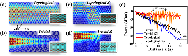
Figure 4. Quantifying the robustness of topological vector edge states. (a) Topological edge state. (b) Trivial edge state. Geometrical parameters: a = 645 nm; r = 180 nm. (c) Topological edge state with Z-type interfaces. (d) Trivial edge state with Z-type interfaces. (d) The power of topological and trivial edge states with and without the Z-type interfaces along the direction of the edge state.
Download figure:
Standard image High-resolution imageIn addition, we notice that the traditional PhC waveguide (figure 4(b)) shows higher loss than the topological waveguide (figure 4(a)), even though they are no bend. The phenomenon originates from the different structures of the two kinds of PhC waveguides. The topological waveguide is constructed by the triangular cylinders and the trivial waveguide by the circular cylinders. Our calculated results show that the imaginary part of the propagation constant in the traditional PhC waveguide is larger than that in the topological waveguide, which results in the higher loss in the traditional PhC waveguide.
3. Topologically protected PBS
In recent years, all-dielectric beam splitting based on the valley degree of freedom is discovered [67, 68]. However, previous works focus on only one polarization mode. In our topological vector edge states, we find that two polarization modes are locked in the different valleys. The different valleys correspond to different propagate directions. Therefore, the topological vector edge state can be used to realize the PBS. Now, we study the topological PBS based on the vector edge state.
The schematic diagram of the PBS is shown in figure 5(a). The footprint of our device is 15 × 10 μm2. The input TE and TM waves are guided along the 250 nm-width wire waveguide to the right part of the PBS device. Some additional designs [43, 49] of the PBS are used to increase the input-coupling and output-coupling efficiency: (1) the intermediate PhC waveguide has been introduced by the overlap of the 560 nm-width waveguide and the edge state. (2) Meanwhile, on the left part of the PBS device, the pillar PhCs are placed near the output port. They are also triangular lattices, with the lattice constant a2 = 400 nm, the radius of the pillars is taken as r2 = 150 nm.
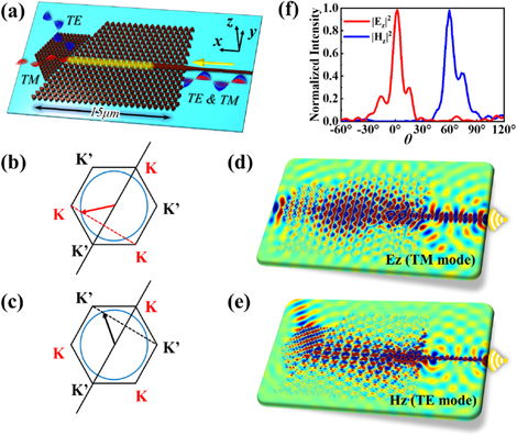
Figure 5. (a) The schematic diagram of the PBS. The k-space analysis on the out-coupling of (b) TM polarization and (c) TE polarization. The blue circle describes the dispersion in the pillar PhCs at λ = 1550 nm. The steady-state distributions of (d) Ez and (e) Hz, corresponding to TM and TE modes. (f) The normalized electric (magnetic) field output intensity in xoy-plane. θ is defined as the angle with the positive x-axis.
Download figure:
Standard image High-resolution imageThe valley edge states will couple into the Gaussian beam of the pillar PhCs [43, 67] near the output port. The direction of the Gaussian beam can be determined by the k-space analysis. As shown in figures 5(b) and (c), the phase-matching conditions [48, 55] can be used to interpret the refraction. The blue circle represents the dispersion in the pillar PhCs at λ = 1550 nm. The black hexagon represents the first Brillouin zone of the TVPCs. For TE and TM edge states, the Bloch wave vectors are respectively locked at K' and K valleys, as exhibited in figures 2(b) and (c). The wave vectors of the TVPCs and the pillar PhCs should be equal on the component in the direction of the boundary, i.e. e·K' = e·k 2 , where e is the boundary direction vector, K' is the wave vector of TVPCs at K' point, and k 2 is the wave vector of the pillar PhCs.
Moreover, we verify the above analysis by numerical simulation. The TM output wave propagates along the red arrow, as shown in figure 5(d). The TE output wave propagates along the black arrow in figure 5(e). The two polarization modes are guided in different directions. That is to say, the topological PBS can be realized.
In figure 5(f), we plot the normalized electric and magnetic field output intensity in the xoy-plane. θ is defined as the angle with the positive x-axis. The results show that the TM wave propagates in the 0° direction, and the TE wave propagates in the 60° direction. These simulation results are consistent with the above analysis. Moreover, we use the extinction ratio (ER) to measure the performance of the PBS with the ER being 10 log(P1/P2), where P1 and P2 represent the output power of TE and TM wave. The ER of the PBS is more than 20 dB in the directions with 0° and 60°.
For more polarization modes, we also study the splitting effect of the PBS with different excitations, including diagonal polarization (TE + TM), and circular polarization (TE + iTM). See Appendix. A for more details.
As shown in figures 6(a) and (b), we put forward two situations of the PBS with the Z-type and the Ω-type topological interfaces. By the simulations of the Z-type interface in figures 6(c) and (e), the TM and TE waves output to the 0° and 60° directions, respectively. The output angle is also determined by the k-space analysis of the TVPCs and the pillar lattices, with the simulation results showing in figure 6(g). Similar to the Ω-type interface, we also study the properties of the PBS, and the simulation results of TM and TE modes are shown in figures 6(d)–(h), respectively. It is noted that PBS works well even though these disorders exist. In order to quantitatively analyze the robustness of the PBS, we calculate the results are provided in appendix
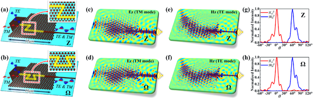
Figure 6. The schematic diagrams of PBS device with (a) Z-type, and (b) Ω-type topological interfaces. (c) and (d) The steady-state distributions of Ez. (e) and (f) The steady-state distributions of Hz. The TM (TE) mode is inputted from the right waveguide to the PBS. (g) and (h) The normalized electric (magnetic) field output intensity in xoy-plane. θ is defined as the angle with the positive x-axis. Additionally, (c) (e) (g) are corresponding to (a); and (d) (f) (h) are corresponding to (b), respectively.
Download figure:
Standard image High-resolution imageFrom the practical viewpoint, if the thickness of the silica substrate increases to more than 100 μm (up to infinite), and the PBS also works. But, the Ge PhCs do not have topological protection. For some disorders like the Z-type and Ω-type interfaces, the robustness of the topological devices usually disappears. So, the thickness of the substrate may increase to infinite when the robustness against the disorders is not necessary.
The PBSs with a very small footprint have been designed using the inverse-designed method. As for our topological PBS, robustness is the highlight. Only the topological devices can work well in some disorders, like Z-type and Ω-type interfaces. The robust performance of topological protection is clearly revealed in our PBS, and it is important in the future photonic integrated circuit.
4. Conclusion
Based on the all-dielectric TVPCs, we have proposed the topological vector edge state and investigated its propagation characteristics by k-space analysis. It is found that the TE and TM edge states are locked in different valleys. Furthermore, we have designed the topological PBS based on the vector edge state. Crucially, the numerical simulations show that the topological vector edge state and the PBS possess robust properties against some disturbances. We believe that compact and robust PBS can find widespread applications in future photonic integrated circuits and quantum information processing.
Acknowledgments
This work is supported by the National key R & D Program of China (2017YFA0303800), the National Natural Science Foundation of China through Grant No. 91850205, and Open fund of the State Key Laboratory of Integrated Optoelectronics IOSKL2020KF23.
Data availability statement
All data that support the findings of this study are included within the article (and any supplementary files).
: Appendix A.
In this appendix, we further study the splitting effect of the different polarization modes, including the single TE or TM mode, the 45° linear polarization, and the circular polarization. As shown in figure A1, the four polarization states are input in the right waveguide, where figure A1(a) corresponds to the single TE mode, figure A1(b) to the single TM mode, figure A1(c) to the circular polarization, and figure A1(d) to the 45° linear polarization, respectively. The simulation results indicate that the PBS can split any polarization mode into the single TE and TM mode.
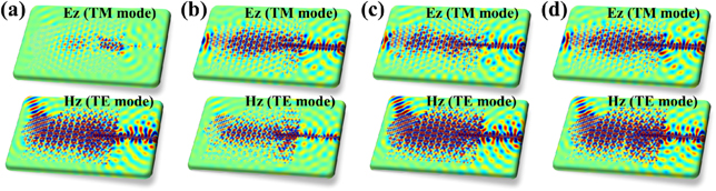
Figure A1. The splitting effect with the different input polarization modes. The input mode is (a) the single TE mode, (b) the single TM mode, (c) the circular polarization TE + iTM, (d) the 45° linear polarization TE + TM.
Download figure:
Standard image High-resolution image: Appendix B.
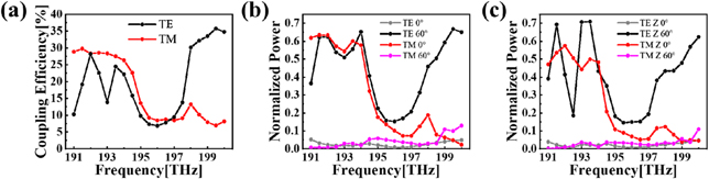
Here, we quantitatively analyze the robustness of the PBS by calculating the total transmissions. In section 3, the connector of the Ge waveguide and the edge state is shown in figure 5(a), and its coupling efficiency is calculated in figure B1(a). The coupling efficiency reaches about 30% around λ = 1550 nm (193.41 THz). Due to the gap of the edge state, the coupling efficiency at 195–197 THz is as low as 10%.
Figure B1. (a) The coupling efficiency between the Ge wire waveguide and the edge state. The normalized power of the PBS (b) without and (c) with the Z-type disorder. In (b), the TE (TM) 60° (0°) represents the detected power of the output port in 60° (0°) with the positive x-axis when the TE (TM) wave is inputted. In (c), Z represents the results are simulated in the PBS with Z-type disorder.
Download figure:
Standard image High-resolution image
And then, we calculate the normalized power of the output ports of the PBS. From 191 THz to 195 THz, the value can reach 0.6, as shown in figure B1(b). With the Z-type disorder, the PBS can also work well around 1550 nm, as shown in figure B1(c).
We have to say that the coupling efficiency and the total transmission are not high. In our further work, the optimization design will be proposed for improving the performance.