


Abstract
Temperature dependent Raman spectra and photoluminescence, as well the Raman mapping of different parts in an individual Sn-doped CdS comb-like nanostructure reveal that the stronger electron–phonon coupling exist at the trunk-branch junctions than other parts. The Huang–Rhys factor was calculated and further confirms that the strong electron–phonon correlation at the junction. The localized deformation from the Sn dopant in the lattice leads to strong electron–phonon coupling at the local junction, which is proved by the scanning transmission electron microscope and energy dispersion spectrum. Moreover, the lifetime of near-band-edge emission and deep-level emission drastically increase with decreasing temperature, which both relate to the localized electron–phonon coupling and relaxation process. This work provides a clear description of the localized carrier correlation in the cross junction part of these branched nanostructures, which can be used to modulate the optoelectronic performance of micro/nanodevices.
Export citation and abstract BibTeX RIS

Content from this work may be used under the terms of the Creative Commons Attribution 3.0 licence. Any further distribution of this work must maintain attribution to the author(s) and the title of the work, journal citation and DOI.
1. Introduction
Micro/nanoscale branched comb-like semiconductor structures have stimulated intensive interest due to their novel properties and potential applications on nanoscale optical and optoelectronic devices [1–4], which extends their structural dimensionality and complexity greatly, providing more functions [5]. In particular, orderly branched nanostructures, such as natural nanowire arrays, will promote the realization of array devices due to their superior array characteristics [6]. Recently, the 2-dimensionally ZnO and CdS comb-like structures with well-aligned branches have been utilized to fabricate high sensitive array sensors and nanocantilever arrays [7–9]. The comb-like Cu2O nanorod-based structures synthesized by an etching method demonstrated great potentials as both electrochemical and gas sensors [10].
One-dimensional (1D) CdS nanowire have shown many unique properties to support their wide applications on waveguide devices, nanosensors, electrically driven lasers, solar cells and light-emitting diodes [11–14]. By integrating noncollapsed, vertically aligned and free-standing nanowires, a good p-n junction occurs in the array structure leading to nanowire-based electrically driven devices [15]. The CdS nanorod/nanowire emitters with better alignment exhibit better field-emission performance [16]. As we know, the intrinsic physical mechanism, such as the carrier transportation and electron–phonon coupling properties, determines the performance of nanodevices. Although the branched nanostructures have shown many unique properties, many carrier related physical behaviors are still unknown [17–19]. Especially for branched nanowire structures, due to the introduction of trunk–branch junctions, this will have a large influence on their physical behavior compared to nanowires.
In this paper, in order to understand the new physical phenomenon of trunk–branch junction lattices, phase transition and electron–phonon coupling inner monolithic comb-like CdS nanostructures, which were synthesized by the reported methods in [20], temperature (78 K–300 K) dependent Raman and photoluminescence (PL) studies have been performed. The local structure related Raman modes and Raman mapping of an individual branched CdS comb-like structure demonstrate that higher Sn doping in the junction induces higher electron–phonon coupling due to rich localized deformation. The temperature-dependent time-resolved PL also reveals that the electron–phonon interaction plays an important role in the radiative recombination. This underlying information from localized CdS comb-like structures will help us to improve array device performance from complex branched structures.
2. Methods
The branched CdS comb-like nanostructures were synthesized by a chemical vapor deposition (CVD) method [20]. A mixture of CdS and SnO2 powders (the molar ratio is about 10:1), loaded in a ceramic boat, was placed in the center of a quartz tube, then the quartz tube was inserted into a horizontal tube furnace. Several Au-coated Si substrates were placed downstream of the source powders at a distance of 11 cm. The high purity argon contained 10% hydrogen, with a constant gas flow rate of 10 sccm, was used as the carrier gas. Then, the furnace was rapidly heated to 1000 °C at a heating rate of 100 °C min−1 and maintained at this temperature for 40 min. After the system was cooled down to room temperature, a yellow product was found to deposit on the ceiling-substrate of the quartz tube. Then the individual CdS comb-like structure was operated to disperse on the Si substrate by a homemade operating probe system.
The morphology and composition of branched CdS comb-like nanostructures were characterized by scanning electron microscopy (SEM), high-resolution TEM (HRTEM) and energy dispersive spectroscopy (EDS). PL and Raman spectra were conducted using a Micro-Raman spectrometer (Acton SP2500, PI and Olympus BX51M) with a 405 nm and 532 nm laser line as an excitation source, respectively. The Raman mapping was measured by a μ-Raman spectrometer (LabRAM HR Evolution, JY Horiba). Time-resolved PL were recorded by the time-correlated single photon counting (TCSPC) system (Picoquant 'Timeharp 200') with a picosecond laser at 405 nm (pulsewidth tens of picosecond) (Picoquant 'PDL 800-B').
3. Results and discussion
Figure 1(a) shows the SEM image of a typical CdS comb-like structure with periodically aligned branches. The branches are evenly distributed at one side of the trunk with a periodic distance of 5 ± 0.5 μm. The diameter and length of branches are around 1 μm and 50–80 μm, respectively. The trunk has a diameter of around 3.3 μm and length of several hundred micrometers. As shown in figure S1 (available at stacks.iop.org/NJP/17/063024/mmedia), Sn droplets can be found at the end of branches, indicating that the formation of the CdS comb-like structure is through the vapor–liquid–solid (VLS) mechanism [21]. Figure 1(b) shows the bright-field scanning transmission electron microscope (STEM) image of one trunk and three branches and junctions. From the STEM image, it can be clearly observed that the branch section and main trunk part show clear and uniform color, which correspond to better structural uniformity with a clean and atomically flat surface, while for trunk–branch junctions, a color difference appears, which means the localized drastically structural variation induces rich deformation in the crystal lattice. To better understand the detailed growth situation of comb-like nanostructure, the high-resolution TEM (HRTEM) of the edge of one branch was obtained, as shown in the figure 1(c). This HRTEM image demonstrates that the branch of the comb-like structure is the wurtzite structure with lattice constants of c = 6.82 Å, without any amorphous sheathed phase along the branch. The lattice constant changes a little compared with that of pure CdS nanostructures due to the incorporation of the Sn dopant into CdS. The branch grows along the [0001] direction, as shown in the figure 1(c). For further investigation of the elemental distribution of CdS comb-like structure at different parts (junction/trunk/branch), the elements of Cd, S and Sn were carried out by EDS analysis, as shown in figure 1(d) and table 1. The Sn element dopant concentration of the trunk–branch junction is much higher than the central part of trunk. The ionic radius of Sn is smaller than that of Cd, so the Sn ions should substitute Cd ions in the CdS lattice rather than by aggregation [22, 23], which induces local deformation at the junction part of the comb-like structure.
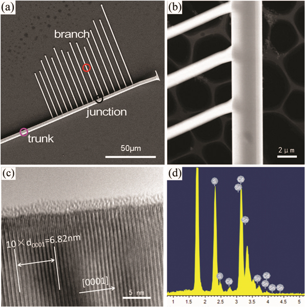
Figure 1. (a) SEM image of a typical CdS comb-like structure. Three different acquisition positions for Raman spectra in the branched nanostructure are marked by different colored circles. (b) The bright-field scanning TEM image of the trunk, branches and junctions. (c) High-resolution TEM image recorded in one branch of the comb-like nanostructure. (d) EDS spectrum from the junction of the individual CdS comb-like structure.
Download figure:
Standard image High-resolution imageTable 1. Comparison of composition at different parts of the CdS comb-like structure.
| Trunk | Branch | Junction | ||||
|---|---|---|---|---|---|---|
| Elements | Atomic% | Weight% | Atomic% | Weight% | Atomic% | Weight% |
| Sn L | 0.23 | 0.38 | 0.37 | 0.63 | 3.2 | 5.30 |
| Cd L | 48.52 | 76.55 | 47.66 | 75.80 | 47.53 | 73.11 |
| S K | 51.52 | 23.07 | 51.97 | 23.58 | 49.2 | 21.59 |
Figure 2(a) shows the room-temperature Raman spectra of CdS comb-like structure from different parts (junction/trunk/branch) marked with colored circles in figure 1(a). The wurtzite CdS structure belongs to the  (P63mc) space group, 9 optical phonon modes and 3 acoustic phonon modes can be deduced by the following irreducible representation [24]:
  According to the multi-peak fitting by the Lorentzian function on experimental curves, as shown in figure 2(a), three peaks at 238 cm−1, 255 cm−1and 303 cm−1 are first-order Raman modes, which can be assigned to the A1 (TO), E2 (high) and LO phonons, respectively [25]. The peaks at 213 cm−1, 290 cm−1, 322 cm−1, 346 cm−1, 366 cm−1, 554 cm−1 and 601 cm−1 originate from multi-phonon Raman scattering. As can be seen, the enhancement of Raman intensity in the junction is stronger than those of other parts under the same measurement condition. Meanwhile, most of the Raman modes of the trunk are slightly red-shift compared to those in the branch and junction parts, as Sn dopant concentration in the trunk is less than that in the branch and junctions. This is ascribed to the incorporation of Sn ions into CdS lattices, a similar phenomenon has been observed in the Ni ion doped CdS nanoribbons [26] and the Sn doped ZnO nanostructures [27].
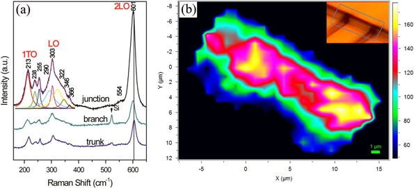
Figure 2. (a) Room temperature Raman spectra of a CdS comb-like structure at different parts (junction/trunk/branch). The Raman experimental data of a junction is the fitting curve using multi-Lorentzian lines. (b) Raman mapping of 1TO phonon mode obtained from local CdS comb-like structure that are marked in the inset.
Download figure:
Standard image High-resolution imageTheoretically, the strength of electron–phonon coupling in semiconductors can be assessed by the intensity ratio of the overtone of phonons to the fundamental (I2LO/ILO). The intensity of the 2LO phonon mode is much stronger than that of the LO mode at the junction, which probably originates from the stronger electron–LO phonon coupling [28]. From figure 2(a), the intensity ratio I2LO/ILO of the junction, branch and trunk in the Sn doped CdS comb-like structure are (∼1.90), (∼1.63) and (∼1.40), which are more than that of nanowires without an Sn dopant (∼1.17) [26]. Moreover, it can be found that the strength of the electron–phonon coupling becomes stronger with increasing Sn doping concentration. At the trunk–branch junction, the electron–phonon coupling is strongest.
Generally, the electron–phonon coupling is governed by two mechanisms: the deformation potential and the Fröhlich potential. The LO Raman scattering cross section depends on both mechanisms while the TO Raman scattering cross section is determined by the deformation potential [29]. The Raman mapping of the 1TO phonon mode and 1LO phonon mode are carried out at the junction and trunk parts, respectively, as shown in figure 2b and figure S2 (available at stacks.iop.org/NJP/17/063024/mmedia). The color bar represents the intensities of Raman scattering. Compared to the intensity of the LO phonon mode, the intensity of the 1TO phonon mode at the junction is much stronger than that at the trunk. The strong electron–LO phonon coupling at the junction is due to more phonons confined in a local space by crystal boundaries or locally deformed defects, which is induced by Sn doping [30]. Therefore, the electron–phonon coupling is enhanced by the deformation potential at the junction, which is consistent with the STEM result. The temperature-dependent Raman spectra of the CdS trunk–branch junction are measured from 78 K to 300 K. Due to the Raman peaks becoming too weak at lower temperatures, the corresponding intensities of Raman curves below 180 K are magnified 3 times in figure 3(a) for clarity. As the temperature decreases, the 1TO (210 cm−1) and A1 (TO) (234 cm−1) Raman modes show almost no shift. While the E2 (high), LO and 2LO modes shift to the long-wavenumber side, together with the full width at half maximum (FWHM) changing, as shown in figures 3(b) and (c). The peaks of the LO and 2LO phonon modes shift to a low frequency around 4 cm−1 and 6 cm−1 with the temperature changing from 78 K to 300 K, respectively. This can be described as the formula [31]:  where χ is the temperature coefficient, which represents the frequency shift of the LO phonon with temperature changing 1 K. The slope of the fitting line represents the value of χ. For the LO and 2LO modes, χ are around −1.97 × 10⁻² and −3.16 × 10⁻² cm−1 K−1, which are larger than that of the CdS bulk [32]. Meanwhile, the FWHMs of LO and 2LO increase with temperature linearly due to the thermal motion of carriers becoming active, then the lifetime of the phonons become shorter.
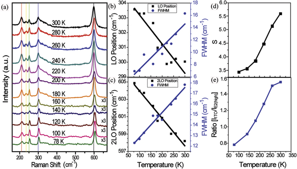
Figure 3. (a) Raman spectra of CdS trunk–branch junction with different temperatures from 78 K to 300 K. The vertical solid lines from left to right represent the 1TO, A1 (TO), E2 (high), LO and 2LO peak positions, respectively. (b, c) Temperature-dependent peak positions and FWHMs of the LO and 2LO Raman active modes. (d) Calculated Huang–Rhys factor (S) versus temperature based on the integrated-intensity ratio of the 2LO to 1LO phonon modes as shown in the abstract graphic. (e) The relative intensity ratio of 1TO to E2 (high) as a function of temperature.
Download figure:
Standard image High-resolution imageThe intensity ratio of the 2LO phonon mode to LO phonon mode is sensitive to temperature. In general, the intensity ratio of 2LO to LO is known to be related to the Huang–Rhys parameter (S) by the relation [29]:

where ω0 is the incident photon frequency, Eex is electronic transition energy, and Γ is the homogeneous linewidth of electronic state. The Eex and Γ can be obtained from the following temperature-dependent PL measurement. As shown in figure 3(d), the I2LO/ILO increases from 1.23 to 1.90 and S changes from 3.54 to 5.60 as the temperature rises from 100 K to 300 K. Figure 3(e) shows the relative intensity ratio of 1TO to E2 (high) as a function of temperature. The intensity of E2 (high) stays stable, while the intensity of 1TO increases with increasing temperature. The S represents the strength of the electron–phonon coupling at the junction part, which reduces with decreasing temperature. The behavior shows that the strong electron–phonon coupling, mainly related to the deformation potential, is obviously enhanced at the junctions. This result also confirmed that the dopant injection will generate a stronger deformation potential, which has been demonstrated clearly by to the result of the Raman mapping [27]. The electron–phonon interaction will reduce with the crystal lattice freezing at low temperatures. Therefore, it can be utilized to control the carrier combination.
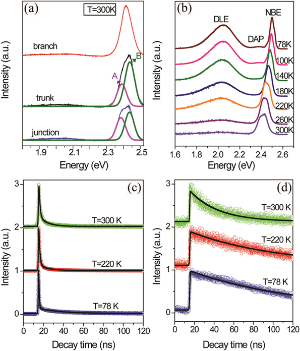
Figure 4(a) shows the normalized PL spectra for three different parts at the branch, trunk and junction, respectively. All the PL spectra include a near-band-edge emission (NBE) band and a deep-level emission (DLE) band at room temperature. For the spectrum from the branch, the NBE band is a single band at 2.42 eV and the DLE locates at 2.01 eV with a broad emission range which is attributed to deep-trap bound states [33]. However, the NBE from the trunk and junction can be fitted well by two Gaussian functions (A and B emission bands) with peaks at 2.39 eV and 2.43 eV, respectively. Figure 4(b) shows the temperature-dependent PL spectra of the junction part with the temperature varying from 78 K to 300 K. Bands A and B show a redshift of ∼110 meV and 90 meV, respectively, while the DLE shows no change during the temperature increase from 78 K to 300 K. The temperature-dependent band-gap shrinkage originates from the expansion of the lattice constant with the rising temperature. A peak is also observed at 2.39 eV at 78 K, which is due to donor–acceptor–pair (DAP) recombination [34]. The intensity of the DAP decreases with increasing temperature and disappears when the temperature increases up to 140 K. The PL intensities of NBE and DLE increase rapidly with decreasing temperature due to the phonon-assisted nonradiative recombination being reduced at low temperatures.
Figure 4. (a) Room-temperature PL spectra at different parts (trunk/branch/junction) of CdS comb-like structure. (b) Temperature dependent PL spectra of the CdS trunk-branch junction. The decay curves of the emissions of NBE (c) and DLE (d) from the trunk–branch junctions of CdS comb-like structures at three temperatures, 300 K, 220 K and 78 K, respectively.
Download figure:
Standard image High-resolution image
The carrier dynamics of the NBE band is investigated to further understand the recombination process. The typical time-resolved PL and the fitted curves are shown in figures 4(c) and (d). The decay curves of NBE can be well fitted by the bi-exponential function expressed as the following [35]:

where Α1 and A2 are the amplitudes and τ1 and τ2 are the decay times. They are summarized in table 2. The short lifetimes τ1 from different parts are 1.05 ns, 1.01 ns, 0.47 ns, respectively, which is ascribed to the delocalized carrier recombination process, and the long lifetime τ2 from different parts are 8.92 ns, 10.40 ns, 21.92 ns should correspond to surface localized carriers at 300 K, 220 K and 78 K, respectively [35, 36]. With the temperature increase from 78 K to 300 K, the short lifetime keeps almost no change while the long lifetime decreases drastically, which is due to a faster exciton decay at high temperatures. In figure 4(d), the DLE decay curve can be fitted with a single exponential decay function with the time constant 21.20 ns, 65.61 ns and 108.65 ns at each temperature, respectively. The experimental results demonstrated thermally activated phonon decrease in the recombination rate at low temperatures, exhibiting the increase of decay time from the DLE band with decreasing temperature.
Table 2. Decay constants and the amplitudes of NEB and DLE at different temperatures.
| NBE emission | DLE emission | ||||
|---|---|---|---|---|---|
| T(K) | τ1 (ns) | τ2 (ns) | A 1 | A 2 | τ (ns) |
| 300 K | 1.05 | 8.92 | 85% | 15% | 21.20 |
| 220 K | 1.01 | 10.40 | 92% | 8% | 65.51 |
| 78 K | 0.47 | 21.92 | 95% | 5% | 108.65 |
4. Conclusion
Sn-doped CdS comb-like nanostructures have been synthesized successfully by the CVD method. We have systematically investigated the temperature dependent Raman, PL and lifetime of localized junction in Sn-doped CdS comb-like structures. The temperature dependent Raman spectra and Raman mappings reveal strong electron–phonon coupling at the junction part with localized deformation, where the doping concentration of Sn is higher than trunk and branch. The temperature dependent PL implies that the phonon assisted NBE emission intensity becomes strong at low temperatures. Moreover, the lifetime of NBE and DLE increases with temperature decrease due to thermally activated phonon decrease at lower temperatures. These results demonstrate that electron–phonon coupling at local trunk–branch junctions from Sn-doped CdS branched nanostructures correlates with localized deformation from higher doping concentrations, which provides new information to further understand the carrier correlation in cross nanostructures. This can be used to modulate the optoelectronic performance of micro/nanodevices.
Acknowledgments
The authors thank Dr Binghui Ge (Institute of Physics, Chinese Academy of Science) for TEM measurements. This work was supported by the National Natural Science Foundation of China (No. 51002011, 21461006, 51472053).