


Abstract
Quantum well states of Ag films grown on stepped Au(111) surfaces are shown to undergo lateral scattering, in analogy with surface states of vicinal Ag(111). Applying angle resolved photoemission spectroscopy we observe quantum well bands with zone-folding and gap openings driven by surface/interface step lattice scattering. Experiments performed on a curved Au(111) substrate allow us to determine a subtle terrace-size effect, i.e., a fine step-density-dependent upward shift of quantum well bands. This energy shift is explained as mainly due to the periodically stepped crystal potential offset at the interface side of the film. Finally, the surface state of the stepped Ag film is analyzed with both photoemission and scanning tunneling microscopy. We observe that the stepped film interface also affects the surface state energy, which exhibits a larger terrace-size effect compared to surface states of bulk vicinal Ag(111) crystals.
Export citation and abstract BibTeX RIS

Content from this work may be used under the terms of the Creative Commons Attribution 3.0 licence. Any further distribution of this work must maintain attribution to the author(s) and the title of the work, journal citation and DOI.
1. Introduction
Vicinal surfaces with arrays of steps are one of the most simple realizations of a self-organized nanotemplate, on which low-dimensional materials and nanostructures can be tailored. They are commonly sought to synthesize one-dimensional (1D) objects by step decoration, such as nanoribbons or nanowires [1, 2], but they are also useful to conveniently alter kinetics and energetics in two- and three-dimensional growth. In fact, surface steps facilitate defect-free, layer-by-layer growth at low substrate temperatures by enabling the step-flow mode, even at very complex heterostructure interfaces [3]. Similarly, using stepped surfaces one can avoid rotational two-dimensional (2D) domain structures of adsorbates, which are forced into a single domain within sufficiently narrow terraces [4–7]. In general, for thin films, using stepped substrates allows one to trigger and/or tune uniaxial properties, such as the magnetic anisotropy and its film thickness dependence [8]. On the other hand, steps are known sources of electron scattering, which, for example, may lead to a significant reduction of the electron mobility in the 2D electron gas at oxide heterointerfaces, resulting in an effective 1D behavior [9].
The aim of the present study is to determine the fundamental electronic properties of a prototype metallic thin film when it is grown on a vicinal surface. The system of choice is Ag/Au(111), which exhibits an abrupt interface and step-flow growth at reduced temperatures, thereby leading to sharp, intense QW states of the Ag  band [10, 11]. Using stepped Au(111) substrates we can test, on the one hand, the nature of bulk-like discrete states for a Ag film oriented along a low-symmetry direction, and on the other hand, the influence of the atomically rough, stepped substrate/surface. For the sake of accuracy, we have grown Ag film wedges on a curved Au(111) crystal surface, as shown in figure 1. The combined wedge/curved surface approach allows us to slowly vary both the film thickness and the step density during angle resolved photoemission spectroscopy (ARPES) and scanning tunneling microscopy (STM) experiments.

Figure 1. Angle-resolved photoemission from Ag QWs on Au(111)-stepped surfaces, following the wedge/curved crystal approach hν = 21 eV. (a) The thickness of the film is precisely selected along the grown wedge (θ direction, dotted line) and then the photoelectron intensity is measured at this point for different miscut (α) angles (ϑ direction, curved line). The accuracy of the approach is demonstrated in the analysis performed at  through panels (b)–(d). (b) Grayscale plot of the photoemission intensity for 11.4 ML of Ag. The surface state and the QW band are independently scaled. Panels (c) and (d) respectively show the layer resolved QW spectra for a 11.0–13.3 ML wedge, and the n = 1 and n = 2 QW band shift for a 7–12 ML wedge.
Download figure:
Standard image High-resolution imageIn ARPES spectra we clearly observe the characteristic signatures of lateral scattering, i.e., the superlattice gaps and the terrace-size effect affecting QW states of Ag films. Based on a simple quantum confinement model for a box with periodically stepped boundaries, we explain the variation of the terrace-size effect of QW states as a function of the step density of the surface/interface. The curved surface approach appears fundamental to prove other subtle electronic effects found in stepped films, such as the tilt of the quantization axis of the bulk band away from the high symmetry direction, as well as the enhancement of the strength in the scattering potential of surface states at step edges of thin films versus bulk crystals. Such enhancement is attributed to the added effect of the stepped Ag/Au interface, to which surface states of thin films with vicinal orientation are more sensitive. Structural information about the source of scattering in such stepped films is obtained by a combined topographic and spectroscopic STM analysis. This reveals a superlattice of defect-free monoatomic steps that is coherently aligned with that at the interface, discarding the presence of strongly reflecting stacking fault planes observed in other Ag films [12]. The local character of the STM probe is also used to decompose the surface density of states into different spectral components, namely 2D superlattice states that disperse along the macroscopic surface and lateral resonances confined on individual terraces.
2. Experiment and theory details
The substrate was a Au single crystal polished with a cylindrical shape, such that the surface spans a full  miscut range away from the (111) direction at the center of the sample, which is therefore defined as a c-Au(111) surface. Such c-Au(111) substrate allows one to explore both {111}-type microfacets (for
  ) and {100} microfacets (for
  . Clean surfaces displayed well-ordered, monatomic (h = 2.36 Å) step arrays along the
 ![$[1\bar{1}0]$](https://content.cld.iop.org/journals/1367-2630/16/12/123025/revision1/njp505416ieqn6.gif) direction, with variable step spacing
direction, with variable step spacing  . The quality of the step array across the crystal was reflected in the sharp low energy electron diffraction (LEED) pattern, as well as in the intense surface state peak [13–15]. Ag was evaporated as shallow wedges along the θ-axis of figure 1(a). During the evaporation, the substrate was held at 150 K, and then the film was post-annealed to 300 K. With this process, one ensures a local homogeneous thickness and a sharp interface with minimum Au/Ag intermixing [16, 17]. Moreover, as reflected in STM images (figure 5), this evaporation procedure leads to a coherent step superlattice at the film surface, which replicates the step lattice of the Au substrate underneath. In ARPES, the quality and the smoothness of the films were judged by the sharpness of the QW peaks as well as by the presence of Umklapp bands in the case of stepped crystals (see figures 1 and 2).
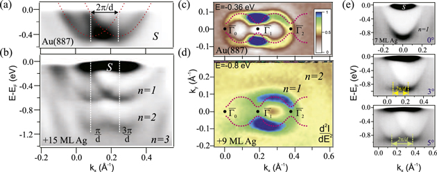
Figure 2. Photoemission intensity plots of Ag films on c-Au(111) ( = 41 eV). (a) Clean c-Au(111), showing the surface state, and (b) 15 ML Ag/c-Au(111), both at α = 3.5° . This miscut corresponds to the (887) surface orientation. Three QW bands with step-lattice Umklapps appear in the latter, which are aligned with the surface state at zone boundaries
  and
and  . (c)–(d) Constant energy surfaces (second derivative) at −0.36 eV, for the surface state of the Au substrate, and at 0.12 eV above the n = 1 QW band minimum (at 0.8 eV), for the 9 ML film, both at α = 3.5°. The crossing of the two Umklapp rings at
  defines a region of lower intensity, revealing a similar gap in both surface and QW states. (e) 7 ML Ag/c-Au(111) QW bands in a ϑ-scan, showing the d-dependent splitting of the n = 1 QW bands.
Download figure:
Standard image High-resolution imageARPES experiments were performed at the Apple PGM beamline of the Synchrotron Radiation Center (SRC) of the University of Wisconsin in Stoughton, using a 2D high-resolution angle resolved hemispherical analyzer. Energy and angular resolutions were set to 30 meV and 0.15°, respectively. The sample was mounted with the steps perpendicular to the slit of the analyzer. This geometry allows us to scan a 80 μm spot across the curved sample with a vertical displacement of the manipulator [ϑ-axis in figure 1(a)], while the channel plate analyzer images the dispersion perpendicular to the steps  at high resolution [figure 1(b)]. In ϑ-scans spectra were taken every 0.2° within the
  range, concretely out of the characteristic faceted region of the Au(111) crystal [4, 13]. STM experiments were performed at 5 K. Differential conductance (dI/dV) spectra were acquired with the lock-in technique, using a bias voltage modulation of frequency 3 kHz and amplitude 20 mV
 . Series of dI/dV spectra were acquired in the direction perpendicular to the steps in order to investigate the quasiparticle interference patterns originated from the lateral scattering.
We used density functional theory (DFT) to help in describing some of the experimentally observed trends in the electronic structure of the Ag/Au system as a function of layer thickness. In particular, by DFT we assessed the sensitivity of QWs to the Au/Ag interface and the change in the bulk-projected band gap for a stepped Ag slab. However, since stepped overlayer systems are beyond current DFT capabilities, the fundamental problem of the lateral scattering of QWs could only be considered within a free-electron-like approach. DFT calculations have been performed using the Siesta method [18]. The Au substrate was represented by a thick slab containing 25 atomic layers. We considered Ag films with up to 15 atomic layers. We did not relax the systems, since the effect of geometric relaxations are known to be rather small for this system, i.e., we assumed a perfect commensuration of the Ag layers on top of Au(111). The in-plane lattice parameter was fixed to that of Au (4.08 Å), while the distance between Ag layers was chosen to keep the experimental volume per Ag atom (an increase of ∼0.5% in the interlayer distance to compensate for the small lateral compression). We used the Perdew–Burke–Ernzerhof functional [19], a 21 × 21 k-sampling and a double-zeta polarized basis set for all atoms, plus one additional layer of ghost atoms in each surface to improve the description of the surface states. The radii of the basis orbitals were determined using an energy shift of 100 meV [18, 20].
3. Results and discussion
The wedge/curved surface approach allows one to carry out very precise measurements, as proved in figure 1. With the ϑ-scan one can accurately determine the (111) surface direction, which is needed for QW energy and emission angle reference, as discussed later. The θ-scan over the shallow wedge determines exact positions for integer ML thickness, as shown in figure 1(c). Here the energy distribution curve (EDC) spectra correspond to the bottom of the free-electron-like band of figure 1(b). They show the characteristic upward shift as a function of thickness shown in figure 1(d), i.e., the (vertical) size effect of an inverted QW [10]. The energies of both the n = 1 and n = 2 QW peaks for each thickness are displayed in the inset of figure 1(d), showing excellent agreement with the latest works in the Ag/Au(111) system [10, 11, 21].
An exotic 2D band topology develops in QW states of Ag films when these are grown on the stepped Au substrate, as shown in figure 2. QW bands of stepped films exhibit the same step lattice scattering signatures observed in surface states of vicinal noble metal surfaces [14, 15], namely Umklapp bands and zone boundary gaps. As for surface states, the photon energy hν = 41 eV is selected to better observe 2D band folding. Figure 2(a) displays an intensity distribution plot of the surface state of clean c-Au(111) substrate, whereas panel (b) shows the electronic states for the 15 ML Ag film, both at α = 3.5°. This miscut corresponds to the Au(887) surface, which is known to exhibit the sharpest array of (38 Å wide) terraces in the whole c-Au(111) sample [13]. In the 15 ML Ag film the intense emission at ∼50 meV binding energy corresponds to the Shockley surface state close to the center of the surface Brillouin zone in Ag(111). The 15 ML thickness allows one to observe the entire dispersion of two QW states (n = 1 and n = 2), and traces of the n = 3. The dashed lines in figure 2 (b) mark the angular position of the minima of QW bands, which coincide with those of surface states of the Au(887) substrate and the Ag film in figures 2(a) and (b), respectively. The momentum scale is referred to the local surface normal α = 3.5° away from the [111]. Umklapp bands for both surface and QWs have minimum energies at  and
and  zone centers. As a consequence successive surface and QW umklapps fold at
  . Figures 2(c) and (d) show constant energy cuts for the stepped Au surface state and for a 9 ML film grown on top, respectively. The displayed
  intensity maps have been acquired at −0.36 eV for the surface state and at 120 meV above the n = 1 band minimum for the QW, i.e., the energies at which surface state and n = 1 QW Umklapps respectively nest. Constant energy surfaces in both cases consist of a double ring structure (dotted lines are added as a guide to the eye) with a depleted intensity around the
  points, indicating the presence of a superlattice gap. Finally, figure 2(e) illustrates a typical ϑ-scan for a 7 ML film. In this case, the zero in the momentum scale refers to the normal emission with respect to the local surface plane in each case. A single n = 1 QW band is observed, which neatly exhibits the miscut-dependent
  Umklapp characteristic of curved surfaces [14].
The proximity in the energy-momentum space of surface and QW states of flat and stepped films is demonstrated in figure 3. We must note the key property of QW states of stepped films found in figure 2, namely their fixed  momentum location. This determines the peculiar
  direction of discretization of the Ag
  band in the
  -space, which is indicated in figure 3(b). In order to keep the constant
  value, the series of n discrete kz values originating at the L point must be located along the bulk
  direction. In panel (a) we analyze bulk bands of Ag calculated along the high-symmetry [111] direction
  and and a low-symmetry
  direction defined by a α = 10° tilt from [111] and towards
 ![$[11\bar{2}]$](https://content.cld.iop.org/journals/1367-2630/16/12/123025/revision1/njp505416ieqn29.gif) . Bands for low and high symmetry directions split away from
. Bands for low and high symmetry directions split away from  and, for the tilted direction with lower symmetry, band degeneracies are lifted at band crossings. For thin films the band continuum breaks up in discrete states. As a way of example, the overlaid dots represent the surface state (at
  ) and the QW energies for a 8 ML thick film. We assume the simplest scenario, namely eight discrete states equally separated between band extrema, i.e., along
  and
and  , which is in general agreement with the observations [10, 11]. Differences in the
  band dispersion for high and low symmetry directions are minimal, and only a relatively small shift in energy and momentum is expected for the same quantum number. In particular, close to
  , where QWs of figure 2 are found. The inset in figure 3(a) zooms out the expected differences for n = 1 in the 8 ML film and α = 4°. Its kz value is reduced, because the
  momentum scale is shorter (nominally
  =
= ), and its energy is slightly shifted by less than ∼+10 meV with respect to the flat film. Such band-topology shift explains in part the terrace size effect that will be later discussed in figure 4.
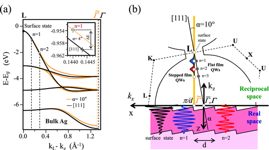
Figure 3. Surface and QW states in flat versus stepped films. (a) Ag bulk band dispersion calculated along high symmetry ([111],  , dark) and low-symmetry (
 -tilt towards [11
  ],
],  , light) bulk directions.
  denotes the extreme point of the
  -bulk band along the α-tilted direction that is closest to
  . Assuming 8 ML thickness, the bulk band is regularly discretized in a series of 8 QW states between
  and
and  (
( ). The inset shows the energy and momentum differences for the n = 1 QW along the [111] (black) and its α = 4°-tilted direction (dashed). (b) Qualitative description of real state wave function (bottom), and reciprocal state location (top) of surface and QW states in a stepped film. X, K, and U stand for high symmetry points of the bulk Brillouin zone, whereas
  and
and  respectively correspond to the edge and the center of the surface reciprocal lattice along kx. In reciprocal space, QW and surface states line up at
  , resulting in distinct series of QW states for flat (
 , filled circles) and α-tilted (open circles) films.
Download figure:
Standard image High-resolution image
Figure 4. Terrace-size effect in QW states of stepped films. (a) n = 1 QW state energy (band minimum) measured in a full  -scan from a 8–12 ML wedge. The upwards shift from α = 0 demonstrates a lateral quantum size effect. (b) Top, potential box model for a stepped film, used to estimate lateral-size effects in QW states within the BEM. Using BEM we obtain the n = 1 QW bands displayed below, which correspond to a θ = 8 ML-thick Ag film with flat (dotted line) and stepped (h = 1 Ag ML, d = 45 Å, solid line) boundaries. The zone-boundary gaps and the upward band shift produced by lateral, repulsive scattering in the stepped film appear indicated. (c) QW energy shift with respect to the (111) direction for all thickness (n = 1 quantum number), obtained from
  -scans (data points). The light-shaded stripe defines the band shift of the n = 1 QW state assuming a fixed value h, but variable d (x axis) and θ (stripe width), the latter between 8 and 12 ML Ag. The dark-shaded stripe adds to this shift the band-topology-shift deduced from the band analysis of figure 3(a).
Download figure:
Standard image High-resolution imageIn the top part of figure 3(b) we qualitatively locate QW and surface states in the ([111]-![$[11\bar{2}]$](https://content.cld.iop.org/journals/1367-2630/16/12/123025/revision1/njp505416ieqn55.gif) ) plane of the reciprocal space. The horizontal, thick solid line schematically represents the
) plane of the reciprocal space. The horizontal, thick solid line schematically represents the  ° -tilted plane, along which kx is defined. The bulk Brillouin zone boundary is depicted with the dashed line, where the corresponding bulk symmetry points are marked. The high and low symmetry directions
  and
and  appear now as thin-dark and thick-light solid lines, with their respective series of QW states, which merge at
  . The latter is found at the characteristic neck of the Fermi surface, which is represented with the curved solid line. For the flat, (111)-oriented film, discrete states align along the [111]-axis, whereas in stepped films QWs arrange parallel to the α-tilted axis. Note that the latter is perpendicular to the surface plane, and hence all, QW and surface states, project with the same
  value. This is the reason why QW and surface state band minima line up at
  in figure 2. In reality, the
  projection point of the band minimum applies for surface states in all vicinal surfaces, regardless of the miscut α [15]. Here we show that the same property characterizes QW states of the bulk s,p-band. In the bottom of figure 3(b) we sketch wave functions of both QW and surface states in real space, as can be deduced from the reciprocal space analysis. Each QW is characterized by a different kz perpendicular momentum [figure 3(a)]. They are confined in the perpendicular direction of the stepped film, and hence delocalized (or 'modulated' [15]) in the average plane of the film surface.
Surface states of stepped substrates are known to exhibit a characteristic terrace-size-dependent energy shift (see [14] and references therein), which reflects the repulsive character of the electron potential at step edges. The presence of a lateral potential with the step periodicity d also affects QW states, as inferred from the Umklapp bands and gaps of figure 2. Figure 4 additionally demonstrates the existence of lateral quantum size-effects, in close analogy with the terrace-size effect observed in surface states. To determine the accurate position of QW bands for each α miscut, we chose a lower excitation energy (hν = 21 eV), which allows us to obscure the  Umklapp of figure 2, and to improve energy and angular resolution in the
  band [14]. Data points in figure 4(a) correspond to the energy of the n = 1 QW band minima across the wedge (θ scan) and as a function of the miscut angle (ϑ scan). These energy minima positions are determined from a systematic line-fit analysis of the whole set of EDC spectra in the full
  -scan7
. All sets of data show a clear step-density-dependent upward shift away from the (111) direction, i.e. from the center of the curved crystal. In figure 4(c) we plot the total energy shift with respect to the (111) direction for the n = 1 QW and across the θ-wedge. It is interesting to observe that the terrace-size shift for QWs appears not to depend, within the error bars, on the film thickness8
.
-scan7
. All sets of data show a clear step-density-dependent upward shift away from the (111) direction, i.e. from the center of the curved crystal. In figure 4(c) we plot the total energy shift with respect to the (111) direction for the n = 1 QW and across the θ-wedge. It is interesting to observe that the terrace-size shift for QWs appears not to depend, within the error bars, on the film thickness8
.
The existence of lateral scattering in QWs of stepped films poses a fundamental question about the nature of the scattering potential. At a bare stepped surface, it is generally assumed that the potential affecting surface states derives from the Smoluchowsky dipole, i.e., from the charge smoothing at the step edge [14]. However, QW states are expected to have a much smaller probability in the surface plane compared to surface states, i.e., QWs are unlikely to sense the surface step dipole. Lateral scattering of QWs could originate from vertical stacking fault planes, which are observed in Ag films [12]. Stacking faults, though, are not likely to appear in large densities in the Ag/Au system, due to the step-flow mode of growth and the excellent lattice matching. Still we cross-check the presence of stacking faults at the film surface using STM. The images in figure 5 correspond to a 6 ML film and illustrate the topography of regions with increasing step density from  3000 Å, to d = 780 Å, and d = 57 Å. In the larger terraces of figure 5(a), high density of dislocations lines can be found. This is in line with studies of Ag films grown on reconstructed Si(111) surfaces, where the lattice mismatch induces a massive formation of ordered stacking fault planes that results in strong lateral confinement [22–25]. However, the density of dislocation lines is dramatically reduced at densely stepped areas of the surface. Already for terraces as large as 780 Å, very few dislocation lines can be observed [figure 5(b)] and, particularly important in the context of lateral scattering, for d below the coherence length of surface electrons, i.e.,
  Å [26], terraces separated by atomic steps appear completely free of dislocations [figure 5(c)].
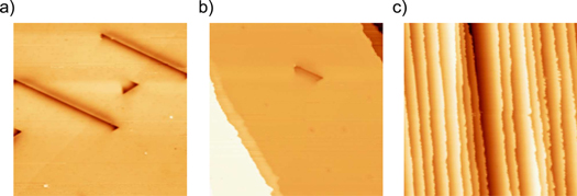
Figure 5. Topographic analysis of a 6 ML Ag film grown on the curved Au(111) surface. The STM images correspond to regions with terraces of width (a)  3000 Å, (b) 780 Å, and (c) 57 Å. Image size: 850 x 850 Å2. Stacking faults easily found in the larger terraces in (a) disappear completely for the small terraces in (c). The latter are of the same size of those exhibiting lateral scattering of QWs in ARPES (figure 2).
Download figure:
Standard image High-resolution imageIn the absence of stacking faults we may consider lateral scattering of QWs at the stepped Ag/Au interface. Although Au substrate steps are covered with Ag atoms, and hence step dipoles are likely to be quenched, the Ag/Au interface defines a periodically corrugated offset of the crystal potential (V), which may lead to a terrace-size dependence in QW energy. However, a precise determination of the QW spectra is needed to address the small terrace-size effect displayed in figure 4(c), and this requires first principles calculations. These are unfeasible due to the extraordinary structural complexity of the stepped Ag/Au(111) system. We may still test the effect of having a stepped crystal potential boundary in QW states within a free-electron like approach, i.e., using the stepped 1D potential sketched on top of figure 4(b). In such system, we have evaluated the scattering of 2D plane-waves using the boundary element method (BEM). BEM has satisfactorily explained the scattering of the Shockley-like surface state in a variety of nanostructures on noble metal surfaces [27–30]. In figure 4(b), the dark area at V = 0 potential represents a thin film of thickness θ, step roughness h, and terrace size d, which is surrounded by a region with higher potential energy V0. The bands below show the results obtained for  , θ = 8 Ag ML, h = 1 Ag ML, and varying the step spacing from d = 20 Å (thick line) to d = 500 Å (dotted line). Compared to the featureless band of the flat (d = 500 Å) film, the QW band in the stepped film exhibits zone boundary gaps (∼18 meV) and shifts upwards (∼6 meV). Both the superlattice gap and the band shift are independent of the crystal potential discontinuity for sufficiently large
  . Based on this observation we have varied d and θ and have obtained the step-dependent size effect shown with the light-shaded stripe in figure 4(c). The dark-shaded stripe is the sum of this size effect and the small band-topology effect discussed in figure 3. The width of the stripes reflects the variation of both effects as a function of θ from 8 to 12 ML9
. We can reproduce the step-density-dependent upward shift, but most of the experimental data lie above the yellow band. This points towards a much larger weight of the QW in the real Ag/Au interface, which cannot be accounted for in the particle-in-a-box approach of figure 4(b).
. Based on this observation we have varied d and θ and have obtained the step-dependent size effect shown with the light-shaded stripe in figure 4(c). The dark-shaded stripe is the sum of this size effect and the small band-topology effect discussed in figure 3. The width of the stripes reflects the variation of both effects as a function of θ from 8 to 12 ML9
. We can reproduce the step-density-dependent upward shift, but most of the experimental data lie above the yellow band. This points towards a much larger weight of the QW in the real Ag/Au interface, which cannot be accounted for in the particle-in-a-box approach of figure 4(b).
In reality, due to the proximity of the Au band edge (at −1.1 eV) one expects a significant weight of the Ag QW wave function at the Au interface. In the top panels of figure 6(a) we show the probability density of the n = 1 QW state in Ag films of increasing thickness grown on Au(111), as determined from DFT calculations. The results completely agree with previous theoretical analysis of the Ag/Au(111) system [10, 11]. Below 10 ML thickness, the n = 1 QW strongly resonates with the Au  band, and above 10 ML, a significant portion of the QW wave function leaks inside the Au crystal. Using the QW wave functions of figure 6(a), we can estimate the thickness-dependent relative weight of the wave function at the interfacial Ag atomic plane. This is shown in figure 6(b). In the thickness range here analyzed, the interface sensitivity is maximum, explaining the large terrace-size shift observed in figure 4(c) that exceeds the estimation of the particle-in-a-box model. For QWs of higher n, the binding energy is closer to the Au band edge and hence we expect the maximum in the interface sensitivity to occur for even thicker films. On the other hand, the increase in the interface sensitivity also affects surface states in the stepped Ag-on-Au films. This is shown in the bottom of figure 6(a) and in figure 6(c), and its origin is discussed next.

Figure 6. Interface sensitivity of QW and surface states in Ag films on Au(111). (a) Top, n = 1 QW probability densities calculated for Ag films of increasing thickness on Au(111). The horizontal scale is centered around the interface, where the QW has a significant weight. Down, surface state probability density in a 14 ML Ag film on a stepped Au(111) substrate of varying α, as determined from a simple exponential decay model (see the text). As the miscut increases, the surface state begins to resonate with bulk states, thereby enhancing its relative probability at the interface. (b) Calculated interface probability density variation for Ag films of increasing thickness on Au(111). (c) Variation of the interface/surface probability density ratio for surface states in Ag films of increasing miscut as a function of thickness, as estimated from the exponential decay model.
Download figure:
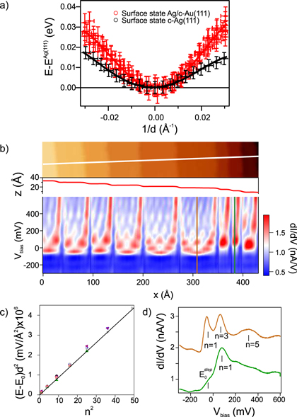
Standard image High-resolution imageThe ARPES analysis of the surface state energy through the curved/wedged film is shown in figure 7(a). We represent the shift of the surface state band relative to that of the center of the crystal, i.e., the terrace-size effect, which is shown compared to the d-dependent surface state shift measured in the curved Ag(111) single crystal [14]. Data points correspond to a 8–12 ML wedge, showing, within error bars, no apparent thickness dependence in this coverage range. In contrast, it is clear that the terrace-size-effect of the surface state in the film is more pronounced than the one measured in the c-Ag(111) crystal. The offset between both curves is of the same order than the lateral size effect measured for QWs [figure 4(c)], suggesting the existence of an additional scattering of surface states by the stepped interface in the Ag film. In reality, the wave function of the Ag surface state decays very slowly inside the bulk, allowing it to reach the interface in the case of a thin film. As discussed below, for a vicinal Ag(111) system (film or bulk crystal) the edge of the projected band gap gets closer to the surface state, and the decay length of the surface state becomes larger. Therefore, for thin stepped films we expect an increasing interface sensitivity of surface states as a function of the miscut angle, and hence an increasing interface scattering contribution to the terrace-size effect, as reflected in figure 7(a).
Figure 7. Analysis of surface states in thin films by (a) ARPES and (b)–(d) STM. (a) Surface state shift for the 8–12 ML Ag/c-Au(111) thin film wedge compared to the terrace-size-dependent shift measured at the surface of the bare curved Ag(111) crystal [14]. (b) dI/dV spectra acquired by STM along the white line indicated in the topographic image displayed on top (the topographic profile is added on the top graph). Setpoint: It = 0.76 nA, Vbias = −1 V. (c) Energy shift (normalized by d2) of the lateral 1D resonances, obtained by fitting the spectra in (b) with Lorentzian peaks. Data are compared to the 1D hard-wall potential expectation (line). Different colors refer to different values of d. (d) Individual dI/dV spectra extracted from the set of (b) (vertical lines). Both spectra exhibit clear 1D resonant peaks. The onset of the dispersing 2D state (E0step) is only visible in the spectra of the smaller terrace (green curve), where it does not overlap with the 1D resonant peaks.
Download figure:
Standard image High-resolution image
We have evaluated the α-dependent increase in the interface sensitivity of thin film surface states assuming a simple exponential decay model [31], where the bulk part of the surface wave function is given by  . The penetration length (
 ) is determined by the energy offset between the surface state (E0) and the edge of the surface-projected bulk gap of Ag (Eedge), as
  . All these magnitudes vary depending on the miscut deviation (α) from the (111) direction. In the first approach, we have determined
  from the projection of the Ag DFT band structure on α-tilted (111) surface planes, and
  from the experimental data [14]. The resulting surface state wave functions are depicted on the bottom panel of figure 6(a) for various miscuts. The corresponding thickness-dependent interface sensitivity, defined as the ratio between the probability at the interface and the surface, is shown in figure 6(c). In the thickness range here examined, the thickness dependence is not strong at any miscut. In contrast, it changes very rapidly from
  miscut up to
  , the latter being the angle at which
  , i.e. the critical miscut at which the surface state becomes a bulk resonance.
Finally, by means of local STM spectroscopy we investigate the interference patterns formed by lateral scattering of surface states in the stepped Ag film. In contrast to other systems, QWs are not detected in dI/dV curves of Ag/Au(111), which is explained as due to the strict surface sensitivity of the STM, plus the small surface probability of QWs at the surface of the Ag/Au(111) system discussed above. The set of dI/dV spectra of figure 7(b) were acquired along the line perpendicular to the steps displayed in the topographic image on the top. Similar to what has been observed in a stepped Cu(111) surface [32], the spectral signal can be decomposed in two contributions: a step-like increase characteristic of the onset of 2D bands, and 1D resonant peaks. The most intense are the 1D resonant peaks originated from the lateral quantization (quantum number n) of the surface state. These can be clearly observed in figure 7(b) and readily attributed to the presence of steps. Both the width and energy of the measured peaks are similar to those found at the surface of stepped Ag(111) crystals [15]. The 1D resonant energies relative to the fundamental onset E0flat = −86 meV (measured for the 2D surface state in a large terrace, i.e., at the center of the curved Ag film) can be grouped independently of the terrace size d, by multiplying the energy shift by d2. The normalized resonant energies are plotted against the square of the quantum number n in figure 7(c). The values are comparable to the energies of the infinite 1D QW (solid line), in the same way as found for stepped Cu(111) [32] and for isolated (non-periodic) terraces in bulk Ag(111) [15]. The 2D contribution to the spectral signal is observed as a weak onset at E0step, and can only be detected in narrow terraces, where it does not overlap with the n = 1 1D resonance. This is the case of the small terraces of figure 5(c), whose  spectrum is shown in the bottom curve of figure 7(d). Such E0step onset is expected to be the STM signature of the dispersing surface state band measured in ARPES [figure 2(b)]. In fact, the shift of the E0step onset relative to the fundamental one (E0step–E0flat = 22 meV), falls within the error bars of that found in ARPES for the same local average terrace size d = 57 Å [see figure 7(a)].The shift of the 2D state in stepped areas therefore relates to the average terrace size, whereas the energies of 1D resonances depend on the local, individual terrace size.
Note that the systematic analysis of the interference patterns shown in figure 7(b) reveals the strict spatial correlation between the 1D resonances and the steps, confirming that the latter are the only scattering source within the Ag film. Moreover, the resonances measured in each terrace are characteristic of a 1D QW with a single, constant reference energy at the terrace, which is given by the E0flat onset of the unperturbed 2D band. E0flat is known to be thickness dependent in Ag films [17], and therefore the constant E0flat reference found in figure 7(b) confirms the lateral homogeneity of the thickness of the film when it is grown on a stepped surface. In contrast, Ag films on flat Au(111) laterally exhibit a clear thickness variation [16]. This means that, under our particular growth conditions (150 K evaporation and 300 K post-annealing), we go beyond the step-flow growth mode, achieving surface steps coherently aligned with those at the interface, as it was supposed for the model of figure 4(b).
4. Conclusions
In summary, in close similarity to surface states, QW states of Ag films grown on stepped Au(111) surfaces display the standard signatures of lateral scattering by the step lattice in ARPES experiments: Umklapps, band gaps, and the terrace-size upward energy shift. These and other characteristic effects, such as the tilt of the quantization axis of the original s,p-band have been accurately rationalized using wedged films and curved crystal substrates, which allow us to smoothly tune film thickness and step spacing, respectively. A simple model of free-electron-like waves confined within a box with periodically stepped boundaries has been shown to qualitatively account for the observed terrace-size energy shift in QW states. The quantitative deviation from such model points to a larger weight of QW wave functions at the Ag/Au interface. Our analysis allows us to conclude that the stepped Au/Ag interface not only dominates the observed lateral QW scattering, but also has a notable influence in the surface state of the thin film.
Acknowledgments
This work was supported in part by the Spanish Ministry of Economy (MINECO) through grants MAT2013–46593-C6–2-P, MAT2013–46593-C6–4-P, MAT2013–46593-C6–5-P, and FIS2010–19609-C02–02, by the German Sonderforschungsbereich SFB 1083, and by the Basque Government through Projects IT-621–13 and IT-756–13. ICN2 acknowledges support from the Severo Orchoa Program (MINECO, Grant SEV-2013-0295).
Footnotes
- 7
Both QW and surface bands have been fitted in the standard way, i.e., a lorentzian peak convoluted with a gaussian, which accounts for the experimental resolution, and a Fermi-Dirac function, which represents the Fermi level cutoff.
- 8
The dependence on the terrace size of the QW energies in figure 4(a) cannot be explained by other phenomena, such as Ag lattice strain, which may modify slightly the QW energy spectrum. Although in the Ag/Au(111) system the lattice strain should be negligible, this may in fact account for an s,p-band shift in the meV range, but that would be rather thickness dependent, and not step-density dependent.
- 9
In the real Ag/Au system, the thickness dependence of the terrace-size effect in quantum well states is expected to be rather complex, because the wave function probability maximum shifts around the Ag/Au interface as a function of thickness, as shown in figure 6.