


Abstract
We analyze a novel antenna effect that resonantly enhances the photocurrent response of end-contacted P–i–N junction nanowire gratings, due to coupling of incident radiation into the grating's multiple-scattering electromagnetic modes. Quantitative characterization of these resonances was performed by spectral and polarization-resolved photocurrent measurements on gratings with N = 500, 200 and 100 nanowires, aided by electron beam-induced current measurements, and in excellent agreement with electromagnetic scattering theory. Despite the small scattering cross-section of each nanowire, with triangular cross-section (height 8 nm, width 6 nm), the measured quality factor of the resonances Q ≈ 10 exceeds that of the empty SiO2 cavity without degradation for gratings of as few as 100 nanowires. Photoresponse retains sinusoidal polarization anisotropy characteristic of single nanowires. We discuss strategies for improving Q and present a grating design tailoring resonant field enhancement at red, green or blue wavelengths, for three different grating periods of ℓ = 460, 400 and 320 nm.
Export citation and abstract BibTeX RIS

Content from this work may be used under the terms of the Creative Commons Attribution 3.0 licence. Any further distribution of this work must maintain attribution to the author(s) and the title of the work, journal citation and DOI.
1. Introduction
Semiconductor nanowires (NWs) are building blocks for future nanophotonic devices [1], and it is well known that their finite size can influence their electronic structure and optical absorption spectrum [2–5]. Additional avenues for engineering the interaction of light with nanostructures include the so-called antenna effects, where the probability of light–matter interaction is enhanced due to coupling of propagating electromagnetic radiation to localized electromagnetic resonances. This strategy has the potential for enhancing the sensitivity and selectivity of NW-based nanophotonic and energy devices [1, 6], and to enhance optical nonlinearities in NWs [7]. Antenna-enhanced photoresponse of single NWs—due to leaky Lorentz–Mie resonances—has recently been reported [8–10], but requires relatively large NWs to achieve enhancement for visible wavelengths, and the resonance wavelength depends on the NW diameter. Recently, a new type of antenna enhancement of NW photocurrent response in the visible regime was reported by Yongshun et al [11], for an array of 500 ultra-small diameter P–i–N silicon NWs (SiNWs) embedded in SiO2, as illustrated in figure 1(A).
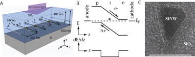
Figure 1. (A) Schematic drawing of Si P–i–N NWs (SiNWs) embedded within 550 nm thick SiO2 layer supported by a silicon substrate. Stars denote electron–hole pair generation and the direction of photogenerated electrons (e −) and holes (h +) toward heavily doped contacts (not shown) is as indicated by arrows. (B) Schematic drawing of band diagram of p–i–n SiNW along the z direction showing transport of photogenerated electrons and holes and electric-field profile for the device. (C) Cross-sectional TEM image of SiNW embedded in SiO2 with base width w ≈ 6 nm and height h ≈ 8 nm (scale: 10 nm).
Download figure:
Standard image High-resolution imageHere, we experimentally determine the wavelength and quality factor of these photoresponse resonances, their dependence on the number of SiNWs for gratings consisting of N = 500, 200 and 100 SiNWs, and the polarization anisotropy of the photoresponse. We also develop a comprehensive quantitative and polarization-dependent theory of coupling of incident radiation into electromagnetic resonances of the SiNW grating. We find that resonances at λ ≈ 420, 490 and 545 nm predicted by our theory match experiments within 5% error and originate from multiple-scattering electromagnetic modes of the grating, with confinement of radiation in a simple dielectric film encasing the grating (see figure 1(A)) assisted by lateral momentum imparted by the grating. The result is resonant enhancement of the absorption efficiency and photoresponse at grating-induced multiple-scattering resonances with Q ≈ 10 independent of the number of SiNWs for as few as 100 SiNWs. While the quality factor falls short of theoretical predictions of Q ≈ 70, most likely due to photon loss from the cavity caused by the NW termination at ohmic contacts, it still well exceeds that of a single NW in the air/SiO2/Si cavity. In agreement with theoretical predictions, the photocurrent response of SiNW gratings retains the sinusoidal electric field polarization anisotropy characteristic of single NWs [12, 13].
As illustrated in figure 1(A), the SiNW grating has both P–i–N doping profile and source/drain electrodes, making it the first reported multiple NW resonance-enhanced and polarization sensitive photodetector. We also further show how the polarization sensitive antenna enhancement can be engineered to occur at a single wavelength in the visible regime, e.g. red, green or blue, simply by changing the period of the grating, for a single SiO2 thickness. Finally, we spatially measure short-circuit current generation along the length of the NW by local excitation with an electron beam, the so-called electron beam-induced current (EBIC) [14]. The EBIC line profile along the SiNW axis demonstrates the regions of the NW where effective charge separation at zero applied bias takes place, and is found in a central segment of length L = 470 ± 50 nm. This coincides well with the expected length of the depleted region supporting a built-in field, which was estimated to be 500 nm from process simulation.
Since each NW acts as a Rayleigh scatterer, resonance wavelengths and Q factors are determined by grating geometry and dielectric contrast at interfaces, while suitable modifications could yield stronger resonant enhancement (Q > 100). These properties may provide advantages over single NW Lorentz–Mie (leaky) resonances [8–10], which are sensitive to NW diameter and, except for very large diameter NWs (d > 100 nm), are limited to modest Q factors. Moreover, the Lorentz–Mie resonances are outside the visible regime for NW diameter d < 25 nm. Finally, d < 10 nm coinciding with the Rayleigh limit is of importance for realizing electronic size quantization in NWs [2, 3] and tunable light absorption/emission in silicon [4, 5].
2. P–i–N array fabrication and structure
SiNW fabrication, described in detail elsewhere [11], was accomplished by top-down fabrication on a silicon-on-insulator (SOI) substrate. Briefly, arrays of N = 500, 200 and 100 parallel rectangular NW fins (width 45 nm, height 120 nm and length 1 μm) were formed by alternating phase shift mask lithography with a KrF scanner, plasma resist trimming and reactive ion etching. The fins were reduced to ultra-small SiNWs by dry oxidation. Phosphorous (≈ 1020 cm−3) and boron (≈ 1020 cm−3) doped regions were formed on opposite ends of the wire by implantation and activated by annealing at a temperature of 1000 °C for 5 s. This process defines a central intrinsic region as one estimated to be 500 nm in length by process simulation, as schematically illustrated in figure 1(B). After removal of the thermal oxide by etching in hydrofluoric acid, SiNWs were encapsulated with 550 nm thick SiO2.
Cross-sectional transmission electron microscopy (TEM) shown in figure 1(C) was also used to examine post-oxidized, ultra-small diameter SiNWs, which sits 150 nm above the Si/SiO2 interface of the SOI substrate. A triangular cross-section of crystalline Si was observed with base width 6 nm and height 8 nm, surrounded by amorphous oxide. The rounded triangular shape is attributed to a non-ideal aspect ratio of the reactive-ion-etched 45 nm wide fins prior to oxidation. Both the triangular shape and rounded corners are consistent with process simulation of the oxidation step that reduces fins to SiNWs. Diced chips were mounted and wirebonded in chip carriers.
3. Results and discussion
Optical photoresponse and EBIC arise due to generation of electron–hole pairs in the P–i–N structure's depletion region and their subsequent separation by the built-in field (figure 1(B)). Before discussing resonant enhancement and polarization dependence of the SiNW array photoresponse, EBIC measurements of the P–i–N are discussed, which have been used to characterize the active region of the device. The junction length extracted from EBIC will be of importance in the analysis of the optical response.
3.1. Electron-beam-induced current imaging of junction
The built-in field region responsible for short-circuit current generation in the SiNWs was imaged by EBIC using a low-noise current preamplifier in a scanning electron microscope. The acceleration voltage and beam current were 8 kV and 100 pA, respectively. A spatial map of the EBIC signal is shown in figure 2(A). Note that the region between the SiNWs corresponds to the reference (zero) level of the EBIC signal. Beginning at the boundary between the cathode and n-type region of the SiNW and moving toward the opposite terminal, the EBIC signal is negative for approximately 250 nm, positive for approximately 500 nm and again negative for approximately 250 nm, for each 1 μm long SiNW. The EBIC profile along a single NW (dashed line in figure 2(A)) is shown in figure 2(B). The width of the bright region at half of the peak EBIC signal is L = 470 ± 50 nm. Bright regions in cross-sectional imaging of junctions are associated with the built-in field where efficient separation of electron–hole pairs occurs [14]. Since the 470 ± 50 nm length of the bright central region matches expected 500 nm length of the intrinsic region, it can be readily attributed to electron/hole pair generation in the intrinsic region.

Figure 2. (A). EBIC image showing seven SiNWs in parallel connected to cathode and anode electrodes. Electron-beam-induced electron–hole pair generation (labeled ⋆) in the depletion region of the SiNW P–i–N junction produces a short-circuit current detected by the ammeter. Scale: 1 μm. (B). EBIC line profile of single SiNW.
Download figure:
Standard image High-resolution imageThe negative EBIC signal (i.e. the P and N regions of the SiNW) occurs by direct injection from the electron beam outside the region of the built-in field [14, 15]. An electron injected directly into the P region would immediately recombine, creating current flow from the anode that would be in the opposite direction to the current generated by electron/hole pair generation in the junction. Similarly, an electron generated in the cathode could recombine with an excess hole from the P region to produce the same response. Stochastic interaction of the electron beam with SiO2 material spatially broadens [14] the electron beam 400 nm below the SiO2 surface, where the SiNWs are located. In particular, this accounts for the blurred appearance of the EBIC image, in which the apparent width of the SiNWs exceeds their physical width.
3.2. Spectral and polarization-resolved photoresponse
Photocurrent I and responsivity  were measured for excitation wavelengths 1100 > λ > 400 nm for 500, 200 and 100 SiNW gratings with no externally applied bias. As shown schematically in figure 3(A), optical excitation was provided by a combination of broadband light source and optical spectrometer, which after collimation was focused onto the sample at normal incidence by an objective lens. An aperture was used to control the illuminated area of the sample, and an electromechanical shutter was used to gate the excitation. Measurements were carried out with both unpolarized and linearly polarized excitation. For the latter, electric field could be oriented at an arbitrary angle relative to the SiNW axis. Chips were mounted on an optical translation stage with three axes of motion. Finally, a moveable beam splitter (BS) was used to image the illuminated area of the sample on a charge coupled device (CCD) camera, as shown in figure 3(A). The diameter of the illuminated area was measured using the CCD to be dm = 520 ± 10 μm. The aperture and translation stage were used in combination to scan the excitation over the large ohmic contacts and wirebonding pads, which, as expected, did not exhibit any short-circuit photoresponse.
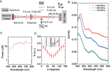
Figure 3. (A) Schematic drawing of optical setup including lamp, optical spectrometer, aperture, moveable BS for imaging illuminated area of sample on CCD camera, final objective lens and chip carrier mounted on xyz translation stage. (B) Measured dependence of responsivity  on wavelength for N = 100 (open triangles), 200 (open circles, offset 0.05 A/W) and 500 (open squares, offset 0.1 A/W), and theoretical fit. Data for 500 SiNWs appear in [11]. (C) Dependence of incident optical power Pm on wavelength. (D) Dependence of
  on angle θ for 200 SiNW grating at 450 nm.
Download figure:
Standard image High-resolution imageIn the short-circuit configuration, I is related to the responsivity  (figure 3(B)) of the SiNW P–i–N junction grating. The total incident optical power Pm shown in figure 3(C) was measured using a calibrated bulk silicon diode. The raw responsivity,
  , was first obtained for an unpolarized excitation. There is a large disparity between the illuminated area Am = πd2m/4 and active area Aa = NWL of N SiNW junctions. Here L = 470 nm is the width of the region where short-circuit generation occurs, as measured by EBIC in figure 2(B). Hence, we define and plot the responsivity
  in figure 3(B) (curves are offset for clarity).
Three distinct peaks at λ ≈ 420, 490–500 and 540–560 nm are apparent in  for N = 500, 200 and 100 SiNWs. These three resonances are not present in the well-known absorption spectrum of bulk silicon [16] and are not the trivial resonances of the bare air/SiO2/Si cavity. Owing to the small cross section of the SiNWs, these peaks cannot be ascribed leaky-mode resonances of individual NWs [8–10], which for d = 10 nm SiNWs in SiO2 occur for λ < 200 nm. Electronic quantum confinement effects in the optical absorption spectrum are also highly unlikely at photon energies of the observed resonances since SiNWs do not have sufficiently small diameter required, typically d ≈ 2–3 nm [17].
However, as we will show, the observed resonances match predictions for scattering of incident radiation into the SiNW grating. Moreover, these resonances occur at wavelengths where radiation is strongly scattered by the SiNW grating, incurs phase from reflection by air/SiO2 and SiO2/Si interfaces and constructively interferes. The resonance quality factor Q determines the lifetime of photons in the cavity. For each of N = 500, 200 and 100 SiNW gratings,  , where
  is the absorption efficiency, was fit to an exponential absorption background appropriate for bulk Si for energies smaller than the direct gap [16], modulated by resonances with center wavelength λi and full-width half-max δλi. Fits are plotted as solid lines alongside measured data in figure 3(B), while extracted curve-fitting parameters and associated uncertainties are summarized in table 1. The quality factor Q of the SiNW cavity is most consistent for the λ1 ≈ 420 nm resonance, with Q = λ1/δλ1 = 11 ± 1, 12 ± 1, 9.6 ± 1 for N = 500, 200 and 100 SiNWs, respectively. Average Q for the three resonances are 13, 16 and 14 for N = 500, 200 and 100 SiNWs, respectively. The Q measured in experiments is an aggregate of different loss mechanisms Qi obeying
  . Since Q is essentially independent of N, we see that losses due to the finite number of SiNWs in the grating do not dominate.
Table 1. Experimentally measured and theoretically predicted free-space wavelengths λi, full-width, half-max δλi and Q-factors. Measurements are given for N = 500, 200 and 100 SiNWs, and theory is given for N → ∞ and N = 20.
| Parameter | Exp. | Exp. | Exp. | Theory | Theory |
|---|---|---|---|---|---|
| N | 500 | 200 | 100 | ∞ | 20 |
| λ1 (nm) | 424±1 | 419±1 | 415±2 | 423 | 422 |
| δλ1 (nm) | 37±2 | 35±1 | 43±3 | 6±1 | 8±1 |
| Q1 | 11±1 | 12±1 | 9.6±1 | 70±10 | 52±2 |
| λ2 (nm) | 493±1 | 510±1 | 513±3 | 490 | 494 |
| δλ2 (nm) | 29±2 | 42±2 | 26±3 | 10±1 | 12±1 |
| Q2 | 17±1 | 12±1 | 20±3 | 50±5 | 41±3 |
| λ3 (nm) | 561±2 | 546±1 | 540±5 | 544 | 548 |
| δλ3 (nm) | 55±6 | 23±3 | 43±8 | 6±1 | 14±1 |
| Q3 | 10±1 | 24±3 | 13±2 | 90±15 | 39±3 |
The measured dependence of  on polarization angle θ is shown in figure 3(D) for the 200 SiNW grating at a wavelength 450 nm between the 420 and 510 nm resonances. It retains the sinusoidal dependence
  that is characteristic of single NWs [12]. We find
  , reflecting more efficient electric field penetration into the SiNW for polarization along the NW's axis compared with the perpendicular polarization. For a single SiNW we expect
  . This value is smaller than the measured ratio
  SiNW grating, i.e. the measured anisotropy falls short of the theoretical prediction.
3.3. Geometrical resonances and quality factors
To better understand the wavelengths and quality factors of the resonances, their dependence on the number of SiNWs in the grating and the polarization anisotropy, we consider the scattering of an incident electromagnetic plane wave Ei into the SiNW grating. The total field E(r,t) so obtained is directly related to  as follows. The time-averaged power dissipated in an electromagnetic field
  due to generation of electron–hole pairs in N parallel SiNWs is given by
  , where j = 1,...,N is the index of an SiNW with junction volume Vj, and
  im is the imaginary part of the NW's complex dielectric permittivity, = re − iim. The short-circuit current at the terminals of the SiNW is therefore I = eηintPloss/ℏω, where ηint is the number of charges collected by the contacts per absorbed photon. For a total incident power
  on N NWs, the responsivity is therefore
  , where

is the absorption efficiency, A is the SiNW cross-section,  is the intensity of optical excitation for an incident plane wave with electric field amplitude E0 and Pj = WLS.
The electric field E(r) in equation (1) for the SiNW structure (figure 1(A)) was estimated by means of electromagnetic scattering calculations for plane waves at normal incidence to both finite and infinite gratings of infinitely long SiNWs for incident electric field parallel and perpendicular to the SiNWs. The finite element method (FEM) was used to calculate E(r) for the case of N → ∞ SiNWs using analytically formulated scattering boundary conditions for light incident from above the structure and periodic boundary conditions at surfaces defined by x = ± ℓ/2. The influence of finite number of N NWs in the array was explicitly addressed for N ⩽ 100, using the so-called perfectly matched layer boundary conditions. Details of the FEM scattering calculations are given in the supplementary information (available from stacks.iop.org/NJP/15/093029/mmedia). An analytic solution for the case N → ∞ and electric field parallel to SiNWs was derived for the limit where the SiNW diameter d satisfies d ≪ λ, and is presented in the supplementary information. The dielectric properties = re − iim of the SiNWs and Si substrate were taken as those of the well-known bulk electronic structure of silicon [16].
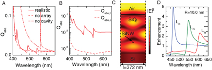
For electric field parallel to SiNWs, calculated  for an infinite grating (figure 4(A), solid line) reveals resonant enhancement for free-space wavelengths λ = 423, 490 and 544 nm for d = 10 nm cylindrical SiNWs. Each of these wavelengths is in good agreement (< 5% error), with each of the grating devices with N = 500, 200 and 100 SiNWs, as summarized in table 1. As shown in the supplementary information, calculated wavelengths for SiNWs were found to be independent of NW cross-sectional shape for a range of cylindrical diameters 10, 8 and 6 nm and triangular cross-sections (W,h) = (13,12 nm). This verifies that for SiNW diameters d/λ ∼ 1/30, the Rayleigh scattering limit can be applied to the structure.
Figure 4. (A) Calculated absorption cross-section  for wavelengths in the visible regime including light scattering by SiNW arrays as well as air/SiO2/Si cavity (solid line), ignoring scattering by SiNWs (dashed), and ignoring scattering by air/SiO2/Si interfaces (dash-dot). (B) Inset: absorption cross-sections
  and
and  for parallel and perpendicular electric field polarizations. (C) Calculated cross-sectional plot of electric field magnitude for a single unit cell of the grating at the 544 nm resonance. Vertical dashed lines indicate periodic boundary conditions, while top and bottom boundaries (not shown) are formulated as scattering boundary conditions discussed in detail in the supplementary information (available from stacks.iop.org/NJP/15/093029/mmedia). The NW position, 150 nm above the Si substrate, is indicated by a black circle. (D) Enhancement of power density inside R = 10 nm SiNWs in 260 nm thick SiO2 for red, green and blue wavelengths, for grating period L = 460, 400 and 320 nm, respectively.
Download figure:
Standard image High-resolution image
The SiNW grating is responsible for the observed resonances, rather than the air/SiO2/Si cavity. Additional finite element scattering calculations in figure 4(A) (dashed line) show that a single NW in SiO2 does not exhibit strong resonant absorption features, due to weak scattering by a single SiNW and poor quality factor of an empty air/SiO2/Si cavity. Nevertheless, the interfaces of the air/SiO2/Si cavity modify the resonance condition when the grating is present, which is an essential ingredient producing agreement between theory and experiments as shown in table 1. Indeed, calculated  for otherwise identical SiNW gratings in an infinite SiO2 medium without interfaces, shown in figure 4(A) (dash-dot), exhibits only a single resonance in the visible regime at the onset (θ = π/2) of the first-order diffraction, l sin(θ) = λ0/nSiO2. The analytical model for multiple scattering of radiation by SiNWs modified by the presence of dielectric interfaces presented in the supplementary information, is in excellent agreement with numerical calculations.
A crucial ingredient determining the sharpness of predicted resonances is that radiation scattered by the SiNW grating and SiO2 interfaces picks up wavevector components 2πn/ℓ along the  direction (figure 1(A)) due to the grating's periodicity, giving multiple scattered radiation grazing incidence on the dielectric interfaces. Radiation is totally internally reflected by the air/SiO2 interface for λ0 > ℓ, and due to its grazing incidence and the high dielectric constant encountered, is strongly reflected at the SiO2/Si interface.
The quality factors predicted for the 423, 490 and 544 nm resonances are given in table 1, which fall in the range Q ≈ 50–90. Photon loss from the calculated modes is mainly due to incomplete reflection at the SiO2/Si interface. Absorption resonances calculated for a suspended SiO2 film (air/SiO2/air cavity) with embedded SiNWs are considerably sharper than those of the same structure supported by the Si substrate. In this situation, diffracted radiation is totally internally reflected at both SiO2 interfaces. Details are provided in the supplementary information (available from stacks.iop.org/NJP/15/093029/mmedia).
The predicted quality factors are on average approximately five times higher than the corresponding experimental values. For the 420 nm resonance, theoretically predicted Q = 70 ± 10 is approximately seven times higher than the corresponding measured value. Since decreasing Q corresponds to decreasing photon lifetime in the cavity, the lower quality factor in experiments suggests a photon loss mechanism that is not accounted for in the calculation. Photon loss, both due to electron–hole pair generation in SiNWs and the silicon substrate, which for the latter occurs due to incomplete reflection at the SiO2/Si interface, was considered in the theoretical calculation and are therefore not responsible for the discrepancy.
We evaluate several possible photon-loss mechanisms to determine the most likely cause of the discrepancy. Loss of photons from the mode by scattering into the continuum at the boundaries of the finite arrays can be easily eliminated as the cause. Theoretical calculations on finite arrays of N = 20 and 100 SiNWs described in the supplementary information give Q = 52 and 70, respectively, while experiments give Q ≈ 11, 12, 10 for N = 100, 200 and 500, that is, consistently smaller quality factors with no significant trend with respect to N. Calculations of  were also carried out for an array with N = 100 SiNWs, incorporating fabrication disorder by adding a random variable to the SiNW position. Even for unrealistically large root-mean-square deviations up to 45 nm, Q could not be significantly suppressed. Halving the cross-sectional area of the SiNW also did not change Q significantly.
Having eliminated photon loss due to finite N and fabrication disorder as the cause of the discrepancy, we attribute the reduction of Q in experiments to end termination of the 1 μm long SiNWs at the electrically conductive ohmic contacts. The SiNWs are not of infinite length as assumed in calculations, and the metal surfaces of the ohmic contact would introduce significant scattering relative to the mode of an infinite length NW. We therefore expect that the quality factor of the resonances can be increased toward the theoretically predicted value by increasing the length of SiNW. Three-dimensional calculations including finite length and contact structures would therefore be of additional interest.
Photoresponse resonances of arrays of NW Rayleigh scatterers could be of interest when large-diameter NWs required for visible wavelength Mie scattering resonances [8–10] are undesirable. Geometrical resonances of the NW array presented herein are determined by the grating period and dielectric environment, and in the Rayleigh scattering limit (d ≪ λ) are independent of d. Large diameters required for visible wavelength Mie scattering resonances would, for example, be incompatible with the realization of electronic size quantization effects in NWs or NW quantum dots [2, 3]. Nevertheless, the multiple scattering resonances of one-dimensional gratings are not incompatible with larger-diameter NWs. Arrays of larger-diameter NWs would also exhibit geometrical resonances related to the array period, although further work is necessary to understand their properties.
3.4. Photoresponse gain
When the number of charges collected by the measurement circuit per photon absorbed (ηint) exceeds unity, we say there is a gain g = ηint. The gain was estimated to be g ≈ 1 from  , using the measured off-resonance zero-bias responsivity
  (figure 3(B)) at λ = 450 nm and the corresponding estimated value of
  (figure 4(A)). This contrasts the biased NW photoconductors without P–N junctions, which frequently [18] have g > 1000. This gain is often attributed microscopically to fast trapping of either photo-generated electrons or holes at surface states, which enhances the lifetime τ of the other carrier. In this case, each carrier of the un-trapped species can effectively transit the device g = τ/τtr > 1 times from one contact to the other, where τtr is the carrier transit time. During this process each carrier of this species is replenished from an ohmic contact g − 1 times [18].
Examination of the band diagram in figure 1(B) shows that the replenishment process that produces gain in biased NW photoconductors is not possible near zero bias for a P–N junction NW. Electron (hole) replenishment is strongly blocked by the P (N) region's ohmic contact. While electron (hole) replenishment is possible by the N (P) region's ohmic contact, transport is blocked by the junctions' built-in potential. This is interesting since gain from this replenishment process comes at the expense of bandwidth, and quenching the gain should increase the intrinsic device speed [18]. If gain is desirable, the P–N junction could, in principle, be reverse biased into an avalanche multiplication regime. Furthermore, a grating of NWs without P–N or P–i–N junctions could still exhibit resonances of  in combination with a photoconductive gain ηint = τ/τtr > 1 at finite bias. It is straightforward to show that the photoresponse would still be governed by
  . Any effect of inhomogeneous electric field on carrier mobility would be absorbed into the transit time τtr, although such effects are unlikely in the ultra-small NWs employed here.
3.5. Polarization response
The absorption efficiency  was also calculated by the finite element scheme for electric field perpendicular to SiNWs and is shown alongside
  in figure 4(B). It is evident that the ideal grating's polarization anisotropy is
  off-resonance. Moreover, the resonances apparently disappear for the
  case. Therefore, the ideal grating's polarization anisotropy is further enhanced on resonance, compared to a single NW. The absence of resonances for
  is essential because in this case, multiple scattered radiation by an SiNW grating does not constructively interfere. However, the measured off-resonance polarization anisotropy
  falls short of the predicted value. The discontinuity presented by the ohmic contacts (separated by only 1 μm) may be responsible for the smaller-than-predicted polarization anisotropy. Refinements to the sample design are likely to be necessary for improving both Q and for enhancing the anisotropy. The position of SiNWs within the mode's spatial field profile, shown in figure 4(C) for λ = 544 nm, could also be optimized.
3.6. Grating period design example
Finally, we demonstrate the ability of SiNW gratings to enhance sensitivity and selectivity of photodetection at a single wavelength in the visible regime (λ0 ≈ 400–700 nm). First, to reduce the number of resonances in the visible regime, the SiO2 thickness is modified to 260 nm from 550 nm. For this dielectric thickness, resonances for red (λ0 ≈ 610 nm), green (λ0 ≈ 540 nm) and blue (λ0 ≈ 460 nm) wavelengths are obtained for grating periods of ℓ = 460, 400 and 320 nm, respectively. The enhancement of photon density for each grating for d = 20 nm is shown in figure 4(D).
4. Conclusions
Measured visible-wavelength resonances in the spectral photocurrent responsivity of ultra-small diameter end-contacted P–i–N SiNW gratings were found to be in excellent agreement with the mechanism of antenna enhancement, due to scattering of incident radiation into geometrical resonances of the SiNW grating. The measured quality factor is Q ≈ 10 at λ = 420 nm for gratings consisting of N = 500, 200 and 100 SiNWs. Theoretical calculations on infinite length NWs revealed a higher quality factor Q = 70 ± 10 than experiments. We attribute this discrepancy to additional photon loss originating from the SiNW's finite (1 μm) length and termination at conductive ohmic contacts. Increasing NW length or scattering at contacts is, therefore, the simplest strategy for increasing the quality factor. For infinite-length NWs, incomplete reflection, at the SiO2/Si interface, is the dominant photon loss mechanism from the cavity, and suspending the structure was found to considerably increase the predicted Q. Sinusoidal polarization anisotropy of photocurrent was observed for linearly polarized radiation, with strongest response for E∥z (z is the direction of the NW's axis), reflecting more efficient penetration of the resonant enhanced field into the SiNW. Finally, we show that field enhancement for an arbitrary wavelength in the visible regime is accomplished simply by choice of the grating period for a constant SiO2 thickness. These observations provide a pathway for engineered, grating-based enhancement of light–matter interaction for one-dimensional NWs and design of NW-based photodetectors with enhanced wavelength and polarization sensitivity. Moreover, the results extend the theory and application of single-NW optical resonances in photoconductors [8–10] to the limit of cooperative scattering for large arrays. Further work is necessary to understand antenna effects in arrays of larger-diameter NWs (outside the Rayleigh scattering regime), which would also exhibit geometrical resonances.
Acknowledgments
JS, CS, SVN, CYC, CS and HER acknowledge financial support from NSERC, CSA, CIPI, OCF and OCE. Rusli ER acknowledges the support from A*STAR Singapore grant no. 092 101 0055.