


Abstract
By angle-resolved photoemission spectroscopy (ARPES) we observe a giant Rashba-type spin splitting in the electronic bulk conduction and valence bands of the semiconductor BiTeCl. This material belongs to the group of bismuth tellurohalides BiTeX (X = Cl,Br,I) which are layered non-centrosymmetric materials with strong spin–orbit interaction. By photon energy-dependent ARPES, we separate the bulk and surface contribution of the electronic structure and show that the tellurium-terminated (0001) crystal surface hosts spin-split two-dimensional surface states. On the chlorine-terminated surface at the opposite side of the crystal no surface states are observed due to photon-induced surface chemistry.
Export citation and abstract BibTeX RIS

Content from this work may be used under the terms of the Creative Commons Attribution 3.0 licence. Any further distribution of this work must maintain attribution to the author(s) and the title of the work, journal citation and DOI.
1. Introduction
A prerequisite for the spin–orbit interaction (SOI) to lift Kramer's degeneracy in non-magnetic materials is that the inversion symmetry of the crystal is broken. This condition is naturally met at crystal boundaries where SOI is the driving force behind the spin splitting of surface or interface states as in the Rashba–Bychkov effect [1] or of the edge states in  topological insulators [2].
The only way that SOI can lift the spin degeneracy of three-dimensional states is when the crystal itself lacks inversion symmetry [3]. Recently, large Rashba-type splittings were discovered in the bulk bands of the materials belonging to the class of non-centrosymmetric bismuth tellurohalides (BiTeX with X = I, Cl, Br) [4–8].
The interest in these materials is related to their possible advantages in building spintronic devices. In addition to the sizable SOI, the low electron density of these semiconducting materials allows for controlling the spin current by tuning the chemical potential by electrical gating or chemical doping [9]. Further, the fact that the large bulk band gaps significantly exceed the thermal broadening at room temperature facilitates to discern surface contributions in transport measurements.
BiTeI was shown to feature not only spin-split bulk bands which result in unusual toroidal Fermi surfaces but also two-dimensional surface states with large spin splitting which are hosted on the two inequivalent surfaces [6, 9, 10]. In this paper, we present angle-resolved photoemission spectroscopy (ARPES) measurements on the related compound BiTeCl. We show that this compound also features a giant bulk Rashba splitting with a significantly larger bulk band gap. In contrast to BiTeI, which has been reported to suffer from stacking faults leading to mixed surface terminations [6, 9], our BiTeCl samples are single crystalline on a macroscopic scale (mm) with well-defined surface terminations. A preserved stacking order along the polar axis is indispensable for transport measurements since spin effects would cancel out in systems with a mixed orientation of quantization axes.
2. Crystal structure
BiTeCl has a hexagonal crystal structure (space group C46v) of alternating layers of chlorine, bismuth and tellurium atoms as illustrated in figure 1(a) [11]. The crystal has no inversion symmetry due to the continuous stacking order of the three atomic layers. In contrast to BiTeI and BiTeBr, the unit cell of BiTeCl is doubled in the c-direction in such a way that the crystal is symmetric under the screw operation composed of a non-primitive translation by c/2 along the hexagonal axis and a rotation of π/3 around the same axis. In other words, C46v is a non-symmorphic space group with the consequence that additional selection rules for the final state in the photoemission process are introduced, which makes the band structure observed with ARPES depend on the Brillouin zone number [12], as will be discussed below.

Figure 1. (a) BiTeCl crystal structure. (b) Brillouin zone of the bulk (solid lines) and the surface (dashed lines).
Download figure:
Standard image High-resolution imageThe weak bonding between the Te and Cl layer provides a natural cleaving plane in the (0001) plane. Owing to the lack of inversion symmetry, an ideal crystal can have two non-equivalent surfaces, with either Te- or Cl termination, determined by the underlying crystal stacking order. For our measurements care was taken to produce chemically pure terminations.
3. Methods
The BiTeCl crystal was grown based on BiCl3–Bi2Te3. The telluride compound was obtained by fusing stoichiometric amounts of elemental Bi and Te at 600 °C. BiCl3 was prepared by the evaporation of a saturated solution of Bi2O3 in HCl acid. The binary compounds were weighed in proportions of 11 mol% Bi2Te3 and 89 mol% BiCl3 which corresponds to the peritectic melting composition of BiTeCl [13]. The charge was then sealed in a growth quartz ampoule under a pressure of 10−3 Torr. After heating to 430 °C at a rate of 20 °C h−1 followed by 1 day of soaking at this temperature the melt was crystallized by a modified Bridgman method [14]. The top part of the resultant ingot contained eutectic, while the bottom part presented an aggregate of layered crystals. According to our x-ray diffraction analysis a major part of the aggregate consisted of the BiTeCl phase, which was selected for the ARPES measurements.
The ARPES measurements were performed at the high-resolution ARPES end station of the surface and interface spectroscopy beamline and at the soft x-ray ARPES end station of the advanced resonant spectroscopies (ADRESS) beamline [15] at the Swiss Light Source using p-polarized light. The measurements were performed on pairs of crystals mounted with a reversed crystal c-axis. Clean surfaces were obtained by cleaving in situ at sample temperatures below 20 K at a base pressure of 10−10 mbar. The surface termination was determined by x-ray photoemission spectroscopy (XPS) of the shallow core levels of Bi, Te and Cl (figure 2). On all measured samples the Cl/Te ratio was constant across the sample surface indicating single domain termination. Crystals with an inverted c-axis always showed opposite terminations and the type of termination persisted after multiple cleavings.

Figure 2. XPS of shallow core levels comparing Cl- and Te-terminated BiTeCl(0001).
Download figure:
Standard image High-resolution imageThe electronic structure calculations were performed within the density functional theory (DFT) formalism as implemented in the Vienna ab initio simulation package [16]. We used the all-electron projector augmented wave (PAW) [17, 18] basis sets with the generalized gradient approximation of Perdew, Burke and Ernzerhof [19] to the exchange correlation potential. The Hamiltonian contains scalar relativistic corrections, and the spin–orbit coupling was taken into account by the second variation method [20]. To simulate the semi-infinite BiTeCl (0001) system we used a slab composed of 24 atomic layers separated by roughly 20 Å vacuum space with the chlorine side (for the Te-terminated surface) or the tellurium side (for the Cl-terminated surface) passivated by a hydrogen monolayer.
4. Angle-resolved photoemission spectroscopy measurements
Figures 3(a) and (b) show ARPES band maps along the Γ–K direction measured with p-polarized light of 20 eV photon energy on a pair of samples with Cl- and Te-termination, respectively. The spectra show sharp band dispersions significantly different for the two samples, without any indication of mixed terminations, in contrast to what was observed for BiTeI [6, 9]. The bulk bands at the Te-terminated surface are rigidly shifted by 140 meV toward higher binding energies when compared to the situation at the Cl-termination due to a different surface band bending.

Figure 3. (a) ARPES measurement at 20 eV photon energy on Cl-terminated BiTeCl with overlaid bulk band structure obtained from DFT calculations. (b) Same as (a) but measured on inversely stacked, Te-terminated BiTeCl. (c) Energy distribution curves from band map (b) at k|| = 0.15 and 0.25 Å−1, the arrows indicate ultra-sharp two-dimensional states. (d) Second derivative of band map (b) for k|| > 0, the arrows correspond to the peaks highlighted in (c). (e) Band maps of Te-terminated BiTeCl at 62 and 66 eV photon energy exhibit an additional broader two-dimensional electron-like state in the conduction band. (f) Schematic illustration of the staircase-like potential at the two pristine (0001) surfaces of a BiTeCl crystal. (g) Schematic band diagram with split-off surface states located in the first three surface triple layers.
Download figure:
Standard image High-resolution image4.1. Tellurium termination
In this section the ARPES signature of the Te-terminated BiTeCl surface will be discussed in more detail. The ARPES band map in figure 3(b) shows several states located on the Te-terminated surface. A set of hole-like surface states with unusually narrow line widths are energetically located on top of the bulk valence band, better resolved in the off-normal energy distribution curves in figures 3(c) and in the second derivative of the ARPES spectrum in figure 3(d). The electron-like state at the Fermi level is also part of a set of surface states; an additional state with weaker intensity and larger line width can be observed on freshly cleaved samples (figure 3(e)).
These findings are supported by DFT calculations which predict surface states to be present at both possible terminations. In the staircase-like potential landscape at the surface that arises from the layered polar crystal structure (figure 3(f)), sets of two-dimensional states split off the bulk bands and localize in the first three triple layers (TL) beneath the surface (figure 3(g)). The calculations in figure 4(a) show the surface state dispersions of a Te-terminated surface where the localization in the first three surface TL is represented by the size of the DFT data points.
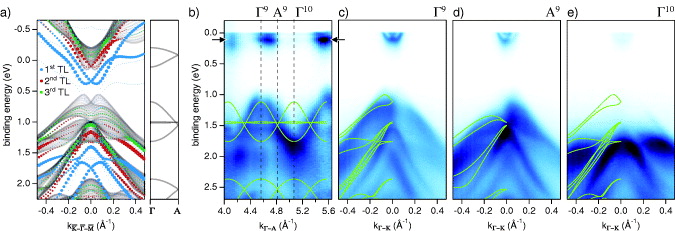
Figure 4. UV-ARPES and DFT spectra of Te-terminated BiTeCl. (a) Left panel: DFT calculations of a Te-terminated BiTeCl slab with bulk bands for different kz (gray) exhibit two-dimensional states in the first (blue), second (red) and third (green) triple layer beneath the surface. Right panel: bulk dispersion along Γ–A. (b) Photon energy scan showing the kz dispersion at normal emission, overlaid with the bulk band dispersion obtained by DFT. (c)–(e) Spectra at selected kz values corresponding to Γ9 (hν ≃ 74 eV), A9 (hν ≃ 83 eV), Γ10 (hν ≃ 93 eV). The differences in spectra observed at Γ9 and Γ10 are related to special matrix element effects, see text.
Download figure:
Standard image High-resolution imageWith ARPES the dispersion of the bulk bands along the out-of-plane momentum kz can be studied by varying the photon energy. Figure 4(b) shows the photoemission spectra along the Γ–A direction (i.e. k|| = 0 Å−1) for a continuous range of photon energies (56–117 eV) measured on Te-terminated BiTeCl. The out-of-plane momentum is obtained by inferring a parabolic dispersion of the photoemission final states in the crystal and neglecting photon momentum transfer. For the inner potential a value of V0 = 5 eV with respect to the Fermi level was obtained.
The two-dimensional state close to the Fermi level (indicated by the arrows) oscillates in spectral intensity, but no dispersion in kz direction can be observed. On the other hand, the kz dispersion of the bulk states in the valence band is evident. The overlaid lines represent the bulk band dispersion as shown in the right panel of figure 4(a). As a striking difference, the spectral features show a periodicity that is twice the size of the Brillouin zone, i.e. compared to what is expected from the hexagonal lattice parameter c = 12.397(1) [11]. The photoemission intensity of each band is suppressed in every other Brillouin zone as a consequence of a special photoemission selection rule in crystals belonging to the non-symmorphic space group, as it is observed in graphite [12] and other materials [21–23]. Experimentally this results in non-equivalent photoemission spectra around the Γ points. Figures 4(c)–(e) show the in-plane dispersion along the  at three neighboring high-symmetry points Γ9, A9 and Γ10. On each spectrum, the DFT bulk band structure around the particular high symmetry k point is overlaid.
As a result of the screw symmetry in the C46v space group the bulk band structure at the A-points features band sticking; at these points all bands are at least two-fold degenerate [24]. The underlying physics is that the structure factor at the A-point vanishes  (ri is the positions of basis atoms) since each atom in the unit cell has a partner of the same atomic species that is shifted by a c/2 translation. Consequently, the Bragg reflection for k around A is suppressed and no band gap opens. The group velocity at the Brillouin zone boundary is non-zero and has the same absolute value for the touching bands due to time-reversal symmetry. This leads to a braid-like band structure in the Γ–A direction, which cannot be experimentally observed due to the above-mentioned photoemission selection rule.
4.2. Chlorine termination
When the BiTeCl crystal c-axis is reversed, the stacking order of the atomic layers inverts and the surface termination changes from a tellurium to a chlorine layer. Time-reversal symmetry, however, ensures that the electronic bulk band structure remains unchanged and only its spin polarization changes sign. Any spectroscopic difference observed in the electronic structure of BiTeCl crystals of opposite stacking orders therefore arises from the different surface terminations.
Figures 5(a)–(d) show ARPES data of Cl-terminated BiTeCl taken in the soft x-ray photon energy regime. The kz dispersion map in figure 5(a) was measured with photon energies in the range from 432 to 825 eV and the band maps in figures 5(b)–(d) were measured at three neighboring high-symmetry points Γ23, A23 and Γ24. Because of the non-negligible photon momentum transferred to the photoelectrons at these high photon energies, the measured electron momenta have been corrected for the photon momentum projected on the particular electron momentum axis. The inner potential was determined to be V0 = 0 eV (with respect to the Fermi level) which is smaller than the value in the UV regime, but consistent with the weakening of the electron exchange-correlation potential for the final states at high photoelectron energies.
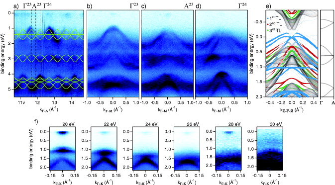
Figure 5. ARPES and DFT spectra of Cl-terminated BiTeCl. (a) SX-ARPES photon energy scan, showing the kz dispersion along Γ–A. (b)–(d) Spectra at selected kz values corresponding to Γ23 (hν ≃ 513 eV), A23 (hν ≃ 535 eV), Γ24 (hν ≃ 559 eV). (e) DFT calculations of a Cl-terminated BiTeCl slab with bulk bands (gray) and the two-dimensional states in the first (blue), second (red) and third TL (green). (f) UV-ARPES band maps for different photon energies.
Download figure:
Standard image High-resolution imageThe measured bulk band structure is in good accordance to what was found for the Te-terminated crystal and the bulk DFT calculations (figure 5(e)), apart from the offsets of the band binding energies. The band gap of about 0.8 eV is in good accordance with ab initio GW calculations [25]. In contrast to the electronic structure of the Te-terminated samples, no two-dimensional state is present neither in the presented photon energy range nor in measurements done in the ultra-violet range, cf figures 3(a) and 5(f). This is clear from the fact that on one hand every observed band can be related to a band in the bulk DFT calculations and on the other hand that the photon energy scans in figures 5(a) and (f) do not feature any sign of a kz-independent state. The DFT calculations in figure 5(e) predict the existence of a set of two-dimensional hole-like surface (blue) and subsurface states (red, green) for Cl-terminated BiTeCl. Equivalent states have been observed on the iodine termination of the related BiTeI compound [6, 9].
In addition, the observed difference in band bending at the Te- and Cl-terminated surfaces is about 140 meV and thus much smaller than the 400 meV predicted by DFT. The relative band bending is obtained by fitting the highest energy bulk valence band to the ARPES data of both terminations and comparing the binding energies.
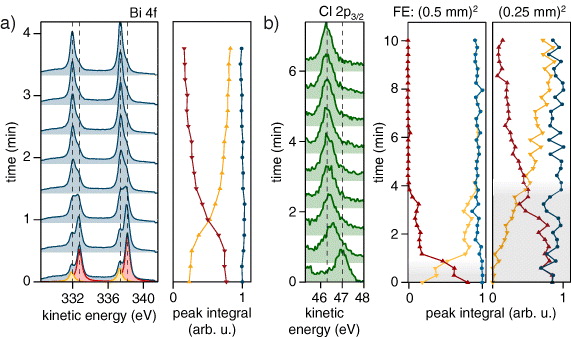
We argue that a chemical process at the chlorine surface induced by the intense synchrotron photon beam is the reason for the reduced size of the band bending and the absence of surface states on the chlorine termination. Figure 6 shows the photoemission spectrum of the Bi 4f state measured with a photon energy of 500 eV. After having positioned the beam spot to a previously unexposed sample area, the 4f levels appear to be split by 800 meV. Under the influence of the photon beam the peak intensity is redistributed to the higher binding energy levels within a few minutes (right panel in figure 6(a)). A similar behavior is observed for the Cl 2p core levels measured with 250 eV photon energy, where the energy difference is about 700 meV (figure 6(b)). The figure shows that the redistribution time scales with the photon flux impinging on the sample, confirming that the core level intensity redistribution at the Cl surface is photon beam induced.
Figure 6. Photon beam-induced core levels shifts. (a) Left panel: Bi 4f core levels shifts. Right panel: background subtracted pristine (red), shifted (yellow) and overall (blue) core level peak integral. (b) Left panel: Cl 2p2/3 core level shift. Right panel: core level peak integrals for two photon fluxes differing by a factor of 8.
Download figure:
Standard image High-resolution image
The Te core levels (not shown) show a similar intensity redistribution due to a changing chemical environment. This is on top of a smaller (200 meV) shift induced by band bending, which is observed in the core level spectra of all the three atomic species. The time scale of this band bending is more than an order of magnitude larger as the one for the chemical change.
5. Discussion
In contrast to Te-terminated BiTeCl(0001), which shows spectroscopic signals of the three-dimensional bulk states and the two-dimensional surface states, all bands observed on a Cl-terminated sample disperse in the out-of-plane direction. The absence of the predicted surface states on the Cl-terminated samples indicates either that the surface states do not form at all or they die out before or during the measurements. We suggest that the states are destroyed by the photon beam which significantly changes the surface chemistry. In this case the absence of the surface states in the ARPES maps just after the start of the light exposure could be related to the higher photon flux used as compared to the XPS measurements, which increases the speed of the chemical reaction.
Given the fact that the core level shifts are only observed on Cl-terminated BiTeCl and that they are largest for Cl and Bi indicates that the chemical reaction takes place in the chlorine layer. A decrease of spectral intensity of the Cl core level cannot be observed, ruling out beam-induced desorption, etching or segregation of the surface. A possible scenario could be the interplay of the photon beam with residual gases of the vacuum, such as beam-enhanced hydrogen adsorption or other photochemical effects of adsorbed molecules on the surface [26].
In the ARPES measurements on the Te-terminated BiTeCl samples no indication for beam-induced ageing is found and the predicted surface states are observed. A remarkable feature of especially the hole-like surface states in the valence band is their small line width down to 40 meV at binding energies of around 1 eV. Such sharp states have also been observed for BiTeI and BiTeBr [6, 7]. Such small line widths at these binding energies indicate small electron-defect and electron–phonon scattering. Considering that these hole-like surface states are energetically overlapping the bulk states, electron–electron interaction can only be small if the surface states are spatially decoupled from the bulk states. The trapping of the surface states in the first surface TL supports such a decoupling but cannot explain why the line width generally decreases for states being hosted in TL further away from the surface. Additional theoretical and experimental effort will be needed to explain this behavior.
6. Conclusion
In conclusion, we have performed ARPES measurements on BiTeCl in the ultra-violet and soft x-ray regime. We observed a large Rashba splitting of the bulk bands of this non-centrosymmetric and non-symmorphic material. The BiTeCl single crystal is either terminated by a chlorine or a tellurium layer, depending on the underlying stacking order. While the Te-terminated surfaces hosts a set of surface states, the theoretically predicted surface states on the Cl-terminated surface could not be observed with ARPES due to a photon-induced change of the surface chemistry.
The large Rashba splitting of both the bulk and the surface states together with the large band gap and the macroscopic crystallinity of BiTeCl make this material an interesting subject for spin transport measurements.
Acknowledgments
We thank E Razzoli, M Radovic, F Dubi, M Kropf and C Hess for their support during the measurements. This work was supported by the Swiss National Science Foundation and the Ministry of Education and Science of the Russian Federation (grant no. 2.8575.2013).