
Abstract
We report the design of a compact dual-polarization on-chip superconductor–insulator–superconductor receiver for array applications. The planar-circuit receiver chip is comprised of the entire radio frequency (RF) signal processing chain with three main circuit components alongside some auxiliary circuits: (1) a polarization splitting 4-probe orthomode transducer (OMT) that couples the RF and local oscillator signal from free space to the chip via a drilled feedhorn; (2) two hybrids that recombine the power of each polarization from the two sets of orthogonal OMT probes; and (3) twin-junction Nb/AlOx/Nb mixers that downconvert the recombined signals to the intermediate frequency. We ensure that the four side walls of each pixel are free from obscuration, using only the top and bottom of the pixel for various connections. Consequently, the design is extendable to a large format array. In this paper, we present the detailed design of the on-chip receiver, including extensive heterodyne simulations and its potential extension into a large format array.
Export citation and abstract BibTeX RIS

Original content from this work may be used under the terms of the Creative Commons Attribution 4.0 license. Any further distribution of this work must maintain attribution to the author(s) and the title of the work, journal citation and DOI.
1. Introduction
Superconductor–insulator–superconductor (SIS) receivers play an essential role in studying the interstellar medium in the frequency regime from 100 GHz to 1 THz [1–5]. These receivers are traditionally configured from two separate single-polarization receivers fed by a polarization-splitting wire grid or waveguide orthomode transducer (OMT) to recover the full signal power and obtain the polarization information of the observed astronomical objects [6–14]. However, this receiver layout makes extensions into larger focal-plane arrays impractical, which is vital for observing large-scale structures in a viable time frame [12–16]. Alternatively, relocating the polarization splitting capabilities onto the SIS mixer chip itself would make the complicated waveguide structures redundant and increase the compactness, which would allow for extending these receivers to a focal plane array.
Although a handful of dual-polarization array concepts exist [12–14, 17], extensions of these concepts to even larger arrays prove difficult since their layout typically occupies space on all sides, making array extensions complicated. Hence, it is vital to locate all accesses at the top and the bottom face of the pixel, leaving the four adjacent sides unobscured to attach additional pixels, as illustrated in figure 1. Although it is challenging to connect all quantities for the mixer operation via two surfaces, similar to [18], the utilization of pixel units following this concept enables a straightforward extension of a single-pixel receiver into a multi-pixel array.
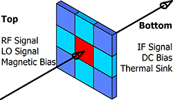
Figure 1. An array configured with nine pixels, which are depicted as coloured boxes. The only available accesses to the central red pixel are the top and bottom faces of the array.
Download figure:
Standard image High-resolution imageIn the following sections, we present this concept with a design centred at 240 GHz with 100 GHz radio frequency (RF) bandwidth, covering the wideband submillimeter array (wSMA) 240 GHz receiver band [11, 19]. This paper first gives an overview of the receiver design and chip topology before presenting the individual on-chip circuit elements. In the fourth section, we simulate the performance of the full receiver chip assembled from these circuit elements. The pixel design in which the receiver chip is deployed is presented in the fifth section together with a 4-pixel example array extension.
2. Receiver overview
Our receiver, shown as a schematic in figure 2, has the entire RF signal processing circuit fabricated on the chip shown in figure 3. A feedhorn and circular waveguide couple the local oscillator (LO) signal and the two free-space RF polarizations, Pol. 1 and Pol. 2, to the on-chip OMT, which separates the polarizations with two sets of opposing probes. The two signals from each pair of opposing probes are recombined with 90∘ hybrids. This routing inevitably leads to the crossover of two transmission lines, which must be carefully designed considering the potential crosstalk between the polarizations. The signals of each polarization recombine at the Σ port of the hybrid, leaving the Δ port isolated. Nonetheless, both ports are connected to mixer circuits, which comprise a bandpass filter (BPF), an SIS mixer, and a lowpass filter (LPF).
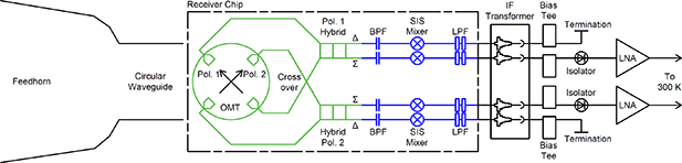
Figure 2. The schematic of the dual-polarization receiver. Components on the receiver chip are shown within the dashed rectangle, with the polarized signal coupling network coloured in green and the mixers circuits in blue.
Download figure:
Standard image High-resolution image
Figure 3. The layout of the dual-polarization receiver chip, 4.0 mm by 4.1 mm in size. The polarized signal coupling network couples both RF polarizations on-chip with the OMT (1) and connects them via the crossover (2) to the hybrids for Pol. 1 (3) and Pol. 2 (4). All hybrid outputs, the Σ port with the superimposed signal of a polarization and the Δ port, which is ideally isolated, connect to identical mixer circuits (5) comprising the BPF, the SIS mixer and the LPF. The mixer circuits lead to bonding pads, approximately 400 µm by 300 µm in size (6), for the IF signal processing. Between these bonding pads leading to the individual mixer circuits are 100 µm by 150 µm ground bonding pads (7), and further 200 µm by 200 µm ground bonding pads are along the sides of the chip (8).
Download figure:
Standard image High-resolution imageThe intermediate frequency (IF) output signal of the receiver chip is wire-bonded to an IF transformer, which matches the impedance of the IF circuit to 50 Ω and accommodates the connectors towards the bottom of the pixel. The following bias-tees inject the DC bias for the mixer operation and connect to either a termination or room temperature electronics via an isolator and a low noise amplifier depending on the preceding hybrid port, Δ or Σ, respectively, as shown in figure 2.
2.1. Receiver chip topology
Our receiver chip is fully planar, formed mainly from microstrip transmission lines. The common microstrip topology eases the design and connection of on-chip circuit elements without transitions to other transmission line topologies while providing a common ground throughout the chip. The circuit is fabricated on a quartz substrate with a relative permittivity  in a 5-step process, summarized in table 1. In the first step, the 14 kA cm−2 Nb/AlOx/Nb trilayer is deposited on all areas covered with the ground conductor. In the second step, the trilayer is etched to the 1.5 µm2 SIS junctions, leaving the bottom layer on the remaining areas to form the 400 nm thick Nb ground-plane layer. After etching, a first SiO layer is deposited in the same fabrication step so that the SIS junctions are self-aligned with the SiO layer and the entire ground-plane layer is covered. In the third step, a second SiO layer is deposited, forming a 200 nm deep 6 µm by 6 µm well where the SIS junctions are exposed to the 400 nm thick wiring layer, which is deposited in the fourth step. In the final step, the bonding pads are coated with 150 nm Au for reliable wire bonding to the chip. After completion of the deposition, the quartz substrate is diced and thinned to 50 µm. Moreover, except for the SIS junctions, all circuit features are designed to be larger than 3 µm to ensure a reliable photolithography process. This, together with the 400 nm thick SiO (
 ) layer, defines a reliably fabricated characteristic impedance of 19 Ω for the microstrips. The superconductivity of Nb at 4.2 K is represented by a frequency dependent surface impedance of a Bardeen Cooper Schrieffer (BCS) superconductor with a Cooper pair binding energy equivalent voltage
  and normal state resistivity
  μΩ cm [20].
Table 1. The 5-step planar-circuit thin-film deposition process.
| Step | Description | Material | Thickness |
|---|---|---|---|
| 1 | Deposition trilayer | Nb/AlOx/Nb | 400/1/200 nm |
| 2 | Etching junctions from trilayer | Nb remains | 400 nm |
| Deposition of first dielectric | SiO | 200 nm | |
| 3 | Deposition of second dielectric | SiO | 200 nm |
| 4 | Deposition of wiring layer | Nb | 400 nm |
| 5 | Deposition of bonding pads | Ti/Au | 10/150 nm |
3. Design of the individual circuit elements
All the individual circuit elements on-chip are designed with Ansys high-frequency structure simulator (HFSS), a three-dimensional finite element method (FEM) solver. In the following sections, we describe the design of each circuit component following the RF signal path of the receiver chip shown in figure 2.
3.1. Orthomode transducer (OMT)
We use a planar OMT to couple the RF and LO signals into microstrips on the receiver chip while separating the two polarizations, similar to bolometric detectors of cosmic microwave background experiments [21–25]. For this setup, the free-space signals couple via a feedhorn into two perpendicular TE11 modes in the ⌀ circular waveguide. These two modes are then guided onto the planar circuit with two sets of opposing probes forming the OMT shown in figure 4. We employ a probe set per polarization so that each probe receives half of the incident signal power of one polarization with 180∘ phase difference between the opposing probes due to the symmetry of the TE11 field distribution.
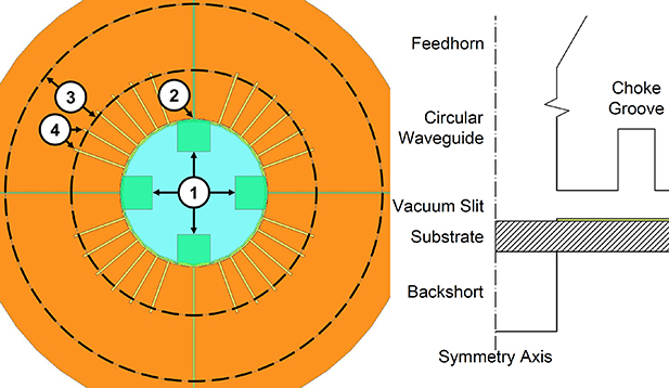
Figure 4. The top view of the OMT on the left and the not-to-scale side view on the right. The OMT probes (1) transform into microstrips at the radius of the circular waveguide (2). The radii defining the choke groove are indicated by (3), and (4) shows the serrations in the ground-plane layer. The width of the microstrips and the serrations are widened for clarity.
Download figure:
Standard image High-resolution imageThe OMT probes are designed to couple maximum power from the circular waveguide with an impedance of a couple of hundred Ohms to the 19 Ω microstrips. The backshort extension of the circular waveguide further enhances the coupling into the probes and, thus, the microstrips.
The presence of the quartz substrate causes reflections of the signal at the interfaces. Although thinning the substrate to 50 µm (which is the practical limit considering the brittleness of quartz) mitigates these effects, the losses are still noticeable. These losses could potentially be minimized using silicon-on-insulator (SoI) technology, but this is still under development in our facilities.
In addition to losses through the substrate, losses also occur in the vacuum slit above the substrate. The slit needs to exceed a minimum height to avoid interference with the on-chip circuit and to accommodate fabrication tolerances, such as the substrate thickness and the machining of the pixel. Balancing the OMT performance with the losses and the uncertainties in the fabrication results in a 50 µm slit.
The losses through this slit are reduced by a quarter-wavelength deep choke groove, machined concentrically at a quarter-wavelength distance from the circular waveguide. This causes the electromagnetic wave in the circular waveguide to encounter an electric short, which prevents a significant fraction of signal power from leaking into the vacuum slit.
Both of the losses discussed above propagate as independent parallel-plate waveguide TEM modes in the substrate and the vacuum slit since these two volumes are separated by the ground-plane layer of the microstrip. The choke groove forms a vacuum-filled parallel-plate ring between the circular waveguide and the choke groove. This ring resonates when an integer number of wavelengths fit into the ring circumference, preventing those signals from coupling into the OMT probes. Adjusting the radius of the circular waveguide and the choke groove changes the ring circumference and therefore offers a method of shifting the resonance to frequencies outside the receiver bandwidth. However, as the resonance is shifted away from the operation band, another order resonance will shift towards the operation band from the other frequency end. Thus, the choice of waveguide and groove radii prevents resonances up to a certain fractional bandwidth. The wSMA specifications of 42% exceed this fractional bandwidth.
To circumvent this problem, Mauskopf et al [26] increased the circumference length of the parallel-plate ring by cutting radial slots between the circular waveguide and the choke groove at a 45∘ angle to the OMT probes, removing the resonance from the frequency band. However, this solution complicates the machining process of the pixel. We therefore disturb the parallel-plate waveguide with radial serrations in the ground-plane layer, shifting the resonance to a frequency outside the band. In summary, we limit the losses through the vacuum slit with a choke groove and suppress the emerging resonances by serrating the ground-plane layer.
Figure 5 shows the simulated response of the OMT. The coupling to the individual probes is essentially identical, leading to a uniform coupling for both polarizations on the chip. This is crucial in order to avoid receiver biases towards one polarization. In addition, the cross-coupling generated by the OMT is less than  . The return loss is reasonable at less than
  , and the total coupling of each polarization into the designated microstrip pair is better than
  . This not-optimal coupling is a consequence of the unavoidable
  loss due to the relatively thick substrate, which can be improved with SoI technology in the near future.

Figure 5. The simulated OMT performance with Pol. 1 responses as solid lines and Pol. 2 as dash-dotted lines. Total coupling denotes the sum over a probe set, and Losses encapsulate the difference between the input and output power measured on all ports.
Download figure:
Standard image High-resolution image3.2. Crossover
Routing the full signal power of each polarization from the OMT to the hybrids inevitably leads to a crossing of two transmission lines carrying different polarizations due to the OMT geometry, which couples the polarizations into the microstrips connected to opposing probes. Therefore, the crossover must be designed to minimize crosstalk between the two crossing transmission lines.
Our planar broadside coupler solution, shown as an inset in figure 6, is largely similar to the design reported in [25, 27] but now at a much higher centre frequency and with lower characteristic impedances. The microstrips are transformed into two coplanar waveguide (CPW) structures in the two conductor layers of the microstrip, namely the wiring layer and the ground-plane layer. In the wiring layer, the CPW is formed from two conductor patches bracketing the 3 µm wide microstrip feed with 3 µm wide gaps over a length of 125 µm, and the ground-plane layer has an opening to deposit the 4.4 µm wide centre strip between the 3 µm wide gaps of the 69 µm long ground-plane CPW. This CPW connects to the feeding microstrip via two 25 µm by 15 µm broadside coupler sets, DC-isolated conductor rectangles in the ground-plane layer and the wiring layer, complying with our 5-step fabrication process. In addition to carefully selecting the broadside coupler dimensions, the performance is enhanced by providing an additional load to the broadside couplers in the wiring layer with the patches bracketing the wiring-layer CPW.
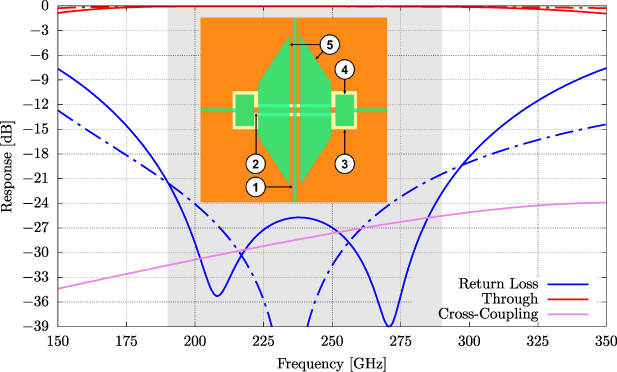
Figure 6. The simulated performance and layout of the crossover. The vertical CPW (1) is routed in the wiring layer, while the horizontal CPW (2) is routed within a gap in the ground-plane layer (3), which connects to the feeding microstrip with broadside couplers (4). Brackets (5) form the wiring-layer CPW, whose response is shown with dash-dotted lines, and solid lines show the ground-plane layer CPW response.
Download figure:
Standard image High-resolution imageThe central conductors for the CPWs overlap less than 15 µm2, leading to the excellent cross-coupling isolation shown in figure 6. This low cross-coupling and return loss yield a high transmission using this compact and easy-to-fabricate crossover design for routing the OMT outputs to the hybrids for recombination.
3.3. Hybrid
Once the two microstrips from an OMT probe set are routed to the same chip location, a circuit element is required to recombine those to feed the mixer with the maximum power available. We abstained from employing a 3-port circuit solution due to the difficulty of implementing power-dissipating circuit elements with our superconducting thin-film deposition process and fundamental impedance mismatches arising from non-dissipative 3-port circuits. Instead, the two-section 90∘ branch-line hybrid shown in figure 7 is implemented to recombine the signal since all four ports of this unidirectional circuit can be matched simultaneously [28–30].
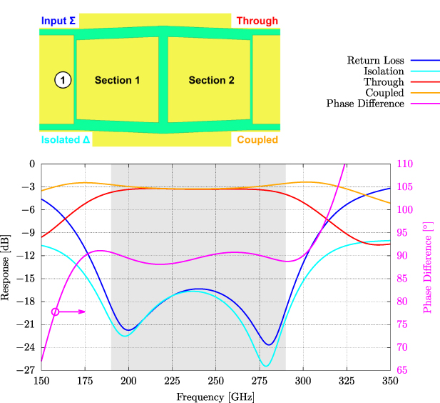
Figure 7. The simulated performance and layout of the two-section hybrid. The performance is shown for an input signal applied on the Σ port. The highest characteristic impedance microstrip (1) is between adjacent ports.
Download figure:
Standard image High-resolution imageThe hybrid branches are approximately quarter-wavelength long microstrips with carefully selected characteristic impedances, with the narrowest 19 Ω microstrips connecting adjacent ports, 5 Ω microstrips leading from the ports to the centre and a 6 Ω microstrip in the centre between the two hybrid sections. The branches are arranged symmetrically in two squares, where the additional section widens the frequency bandwidth, as shown in figure 7.
An input signal at the Σ port couples at  to the Through and Coupled port with a 90∘ phase difference while leaving the Δ port isolated. As the branch-line hybrid is unidirectional, two identical signals with 90∘ phase difference applied at the Through and Coupled port consequently superimpose on the Σ port constructively while superimposing deconstructively on the Δ port. Hence, the hybrid is suitable for recombining the signals splitting between an OMT probe set.
3.4. Bandpass filter (BPF)
Each hybrid output connects to the SIS mixer via a BPF, preventing IF signals from leaking into the RF circuit while maximizing the IF power output. Furthermore, the BPF isolates the DC bias of the individual SIS mixers while passing the RF signal from the hybrid output to the SIS mixer. In this way, we can DC bias each SIS mixer independently.
The BPF design, shown in figure 8, utilizes broadside couplers to route the signal from the 3 µm wide microstrip into a 80 µm long CPW deposited within an opening in the ground-plane layer leaving 5 µm wide gaps, similar to the crossover. Again, a 72 µm by 25 µm conductor patch on top of the CPW is deposited to improve the coupling of the broadside couplers. Consequently, the RF couples efficiently from the hybrid to the following SIS mixer with close to 0 dB coupling and without DC and IF leakage from the SIS mixer into the hybrid.
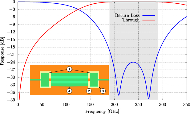
Figure 8. The simulated performance and layout of the BPF. Broadside couplers (1) link the feeding microstrip and the CPW (2), deposited within an opening in the ground-plane layer (3) and covered by a conductor patch in the wiring layer (4).
Download figure:
Standard image High-resolution image3.5. SIS mixer and LPF
SIS junctions suffer from a high geometric capacitance, and this capacitive impedance needs to be matched to the embedding circuit. Although a single junction's impedance can be tuned with a series of stubs, we opted for a twin-junction tuning circuit in which two SIS junctions are connected in parallel with a microstrip section [31], as shown in figure 9. Additionally, a 139 µm long and 9 µm wide series microstrip transformer is added in front of the twin-junction circuit to improve the impedance matching to the circuit prior to this SIS mixer circuit over the full bandwidth.
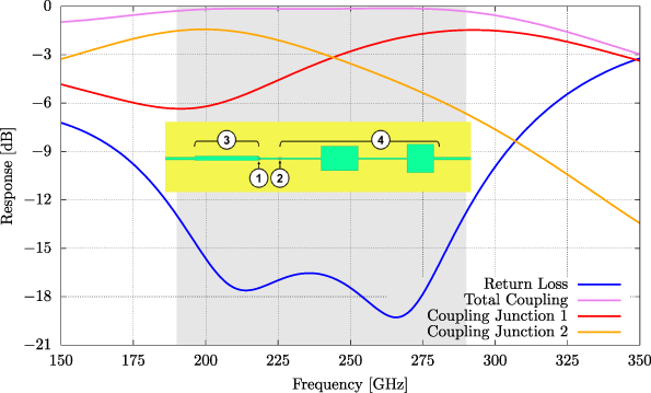
Figure 9. The simulated performance and layout of the SIS mixer and LPF. The SIS mixer consists of a twin-junction circuit, with the first SIS junction (1) closer to the RF circuit and the second SIS junction (2) after an intermediate microstrip. The RF circuit is connected to the twin-junction circuit via a serial impedance transformer (3) and the IF circuit via the LPF (4). Total coupling denotes the sum over both junctions.
Download figure:
Standard image High-resolution imageThe downconverted IF signal is routed to the bonding pad via a microstrip connected to the second SIS junction. This microstrip would also pass considerable RF power to the bonding pads, reducing the power available for downconversion at the SIS junctions. Therefore, the second SIS junction is connected directly to a LPF, which consists of alternating high- and low-impedance, 3 µm and more than 50 µm wide microstrip sections to choke RF signals while passing IF signals. This circuit, feeding the IF to the bonding pad, has an associated input impedance, which alters the RF tuning of the twin-junction circuit. Hence, the twin-junction tuning design must account for the LPF circuit.
The tuning circuit shown in figure 9 comprises two circular 1.5 µm2 SIS junctions with 13.3 Ω dynamic resistance and 120 fF geometric capacitance separated by a 46 µm long 18 Ω microstrip section. The LPF reflects the RF signal power so that more than  of the incoming RF power couples into the two SIS junctions and less than
  couples through the LPF. Both SIS junctions couple close to
  of the input power at the centre frequency, while on each end of the band, the signal couples to one of the junctions predominantly.
4. Layout of the receiver chip
The chip, shown in figure 3, is too large to simulate as a single circuit in HFSS, especially since the waveguide and planar circuit components differ substantially in dimensions. Therefore, we split the receiver into two sub-circuits similar to traditional receivers: first, the polarized signal coupling network shown in figure 10, routing signals from the OMT to the hybrids for each polarization via the crossover; and second, the mixer circuit shown in figure 12, comprising the BPF, SIS mixer and LPF. The mixer circuits connect to all four hybrid outputs of the polarized signal coupling network, similar to mixer blocks attached to waveguide OMTs in traditional receivers.
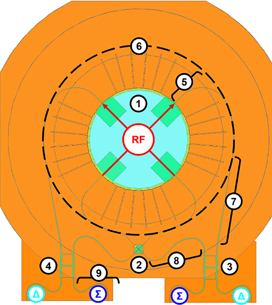
Figure 10. The polarized signal coupling network contains the OMT (1), the crossover (2) and two hybrids, which connect to the ground-plane-layer CPW of the crossover for Pol. 1 (3) and the wiring-layer CPW for Pol. 2 (4). Each OMT probe connects via a straight and an arced microstrip section (5) to the routing concentric to the OMT (6). From this concentric routing, the non-crossing microstrips, connecting the upper two probes, lead via a straight section and a curved section into the straight feeds of the hybrids (7). The crossing microstrips, connecting the lower probes, lead from the concentric circle via an arc section to the straight feeds of the crossovers and afterwards via seven arcs to the hybrids (8). The hybrid outputs are curved to space out the following mixer circuits (9).
Download figure:
Standard image High-resolution imageWe first lay out these sub-circuits within HFSS and then interconnect these structures with Ansys Circuit, a software that applies transmission line theory to the scattering parameters generated by the HFSS models. Thus, a single FEM analysis of the mixer circuit is sufficient in lieu of incorporating four identical mixer circuits as a large model. In the final step, we apply Tucker's theory [32] to predict the receiver gain and noise temperature, using the SuperMix library [33] and the same circuit representation as in Ansys circuit.
4.1. Polarized signal coupling network
The polarized signal coupling network, shown in figure 10, contains the OMT, crossover, and two hybrids. The crucial parameter in this circuit is the microstrip length between the OMT probes and the hybrid input ports. To ensure that the full signal power of one polarization recombines at the Σ port of the hybrid, the microstrip lengths adjust the 180∘ phase difference between a set of opposing OMT probes to the 90∘ phase difference at the inputs of a hybrid by having a length difference equivalent to a quarter-wavelength at the centre frequency.
Moreover, the routing of the two polarizations is symmetric to avoid undesired biases towards one polarization due to loss differences introduced by, for example, the dielectric. Therefore, the crossover is placed at the centre between OMT probes, and the hybrids are located symmetrically with respect to the centre line formed by the OMT and crossover. Furthermore, the hybrids are arranged in parallel to this centre line so that their outputs lead to the same chip edge at which all mixers can be connected to the IF transformer, keeping the receiver compact.
We designed the transmission lines connecting the OMT to the hybrid with straight and curved microstrip lines to avoid corner discontinuities and to reduce the total microstrip lengths. To make the optimization of the design feasible, we first chose a suitable geometry with which all microstrips could be restricted except the straight sections connecting to OMT probes and the following arc, which leads into a concentric circle centred at the OMT, as shown in figure 10. We then fine-tuned the 90∘ phase difference by varying the length of the straight microstrip sections connecting the OMT probes and the radius of the following curved section, keeping the radius of the OMT-concentric circle, the position of the crossover, and hybrid fixed.
Table 2 summarizes the physical lengths of the microstrips connecting the OMT probes and the hybrids in figure 10, which are routed at the crossover in the ground-plane-layer CPW for Pol. 1 and the wiring-layer CPW for Pol. 2. The length of the microstrips routed via the crossover is approximately a quarter-wavelength shorter than that of the uncrossed microstrips; thus, the Σ ports of the hybrids are closer to the OMT-crossover centre line.
Table 2. The microstrip lengths connecting the OMT and the hybrids.
| Pol. 1 | Pol. 2 | |||
|---|---|---|---|---|
| Uncrossed | Crossed | Uncrossed | Crossed | |
| Length | 2128 µm | 1884 µm | 2115 µm | 1871 µm |
| Crossover length | N.A. | 100 µm | N.A. | 125 µm |
| Total length | 2128 µm | 1984 µm | 2115 µm | 1996 µm |
| Difference | 144 µm | 119 µm | ||
In addition to adjusting the phase difference at the hybrid inputs, all circuit elements are impedance matched to avoid reflections, maximizing the signal power coupling to the mixer. Both the OMT and the crossover connect to 19 Ω microstrips, requiring no intermediate impedance transformer, whereas 9 Ω microstrips connect the hybrid. Consequently, the microstrips connecting the OMT and crossover to the hybrids are designed as 5-section binominal impedance transformers [29]. Similarly, the hybrid outputs are constructed from 3-section binominal impedance transformers to match the BPF in the mixer circuit, which again is fed by a 19 Ω microstrip.
The simulation in figure 11 shows that both polarizations couple almost identically with approximately  to their designated Σ ports. In fact, the cross-coupling between the two Σ ports, corresponding to contamination of the two polarizations, is less than
  . Furthermore, the low coupling level into the Δ ports suggests that the circuit is indeed tuned to a 90∘ phase difference at the hybrid inputs. Similarly, the general behaviour of the OMT remains unchanged apart from the expected addition of return loss poles and a slightly higher return loss level, which can be attributed to the addition of impedance transformers and circuit elements such as the hybrid. In summary, the polarized signal coupling network reliably separates the polarizations and recombines the signal power into a single microstrip throughout the desired frequency band.

Figure 11. The simulated performance of the polarized signal coupling network with the Pol. 1 responses as solid lines and Pol. 2 responses as dash-dotted lines. Σ and Δ denote the coupling to the respective hybrid ports.
Download figure:
Standard image High-resolution image4.2. Mixer circuit
The polarized signal coupling network outputs connect to the mixer circuit, comprising the BPF, the SIS mixer and the LPF. We employ these filters so that the RF signals can propagate via the BPF to the SIS mixer for downconversion but not through the LPF, and the downconverted IF signal can only propagate through the LPF.
Figure 12 shows that the BPF connects to the RF input of the SIS mixer via a 3-section impedance transformer to match the 19 Ω output of the BPF to the 12.5 Ω input of the SIS mixer circuit. The impedance transformer and the LPF are meandered to decrease the footprint of the mixer circuit, while the twin-junction circuit of the SIS mixer is on a straight microstrip section. This layout can be fitted to the polarized signal coupling network while maintaining compactness and symmetry. Likewise, the LPF output is angled compared to the feeding microstrip to achieve even spacing between the bonding pads in the layout of the whole receiver chip.
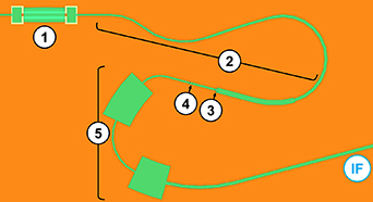
Figure 12. In the mixer circuit, the BPF (1) connects to the SIS mixer via a 3-section impedance transformer (2). The first (3) and second (4) junctions are followed by the LPF (5), which leads to the IF output.
Download figure:
Standard image High-resolution imageFigure 13 shows the power coupling from the junctions to the IF and RF ports as a function of frequency. Adding the BPF to the SIS mixer and LPF introduces poles in the return loss, but none of these poles peak above  within the operation band. The main characteristics of the coupling into the individual junctions remain unchanged at the RF range. In fact, the addition of the BPF reduces the total coupling by less than
  while introducing a
  isolation between the RF and IF port throughout the shown IF and RF range. At low IF, each junction couples
  to the IF output, and the total coupling summed over both junctions only drops below
  above 30 GHz, suggesting the potential broad IF bandwidth of our receiver.

Figure 13. The simulated performance of the mixer circuit. At IF, the parameters, such as the return loss, are referred to the IF port of the circuit, and at RF, the parameters are referred to the RF port. Total coupling denotes the sum over the individual junctions.
Download figure:
Standard image High-resolution image4.3. Performance of the full receiver chip
The performance of the entire receiver chip, shown in figure 14, is simulated by connecting the polarized signal coupling network to four mixer circuits in Ansys circuit. The IF response is identical for all four mixer circuits, and the polarized signal coupling network does not affect the IF behaviour, indicating a well-functioning BPF. At RF, both polarizations continue to behave similarly, without any bias towards a particular polarization. In fact, adding the mixer circuits introduces only extra return loss poles without overly increasing the return loss level and increases the coupling into the Δ mixer circuit by less than 2 dB. The coupling level from the circular waveguide to the designated Σ mixers is around  , dominated by the OMT losses, as explained earlier. The cross-coupling level between the two polarizations remains below
  , mirroring the behaviour of the polarized signal coupling network.

Figure 14. The simulated overall performance of the polarized signal coupling network connected to four mixer circuits, representing the full on-chip receiver. At IF, the parameters are referred to the four IF ports for which the performance is identical. At RF, the parameters are referred to the circular waveguide port with Pol. 1 as solid lines and Pol. 2 as dash-dotted lines. Total coupling denotes the sum over the individual junctions.
Download figure:
Standard image High-resolution image4.4. Gain and noise temperature analysis
We analyse the mixer gain and noise temperature of our receiver using a circuit model similar to the Ansys circuit setup, with a C++ script based on the SuperMix library [33]. The circular waveguide has a frequency-dependent port impedance following HFSS simulations, but now we also employ a standard impedance matching circuit to match the on-chip circuit to 50 Ω. We chose the LO power and DC bias in order to maximize the double-sideband (DSB) mixer gain at 5 GHz IF. Figure 15 shows the optimized DSB mixer gain, the sum of lower-sideband and upper-sideband gain, and preliminary predictions for the noise temperature. Again, both polarization states have an almost identical response. The DSB gain approaches 0 dB, and the DSB noise temperature is between two and three times the quantum limit  . We want to emphasize that the noise temperature values shown in figure 15 are much lower than expected in the real experiment since they do not include losses of several receiver components such as optics; therefore, they only need to be used as a guide.

Figure 15. The simulated DSB mixer gain and noise temperature over LO frequency with Pol. 1 responses as solid lines and Pol. 2 as dash-dotted lines.
Download figure:
Standard image High-resolution image5. Design of the pixel and multi-pixel array extension
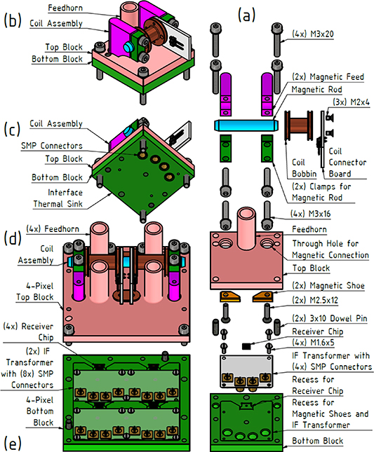
Figure 16(a) shows the interior of our pixel in the explosion view. The receiver chip sits on a pedestal in the bottom block, where the bonding pads are adjacent to the IF transformer. The IF signals are connected from the chip to the IF transformer via bond wires and are then directed to the bottom of the pixel via panel-mount SMP connectors. For practicality, the IF transformer size has plenty of margins to accommodate different circuit designs. We can further reduce the IF transformer and, consequently, the pixel size in a future design refinement once the IF transformer design is finalized.
Figure 16. The explosion view of the pixel (a) and the assembled pixel viewed from the top (b) and the bottom (c). The 4-pixel array extension separated in the (d) top and (e) bottom block assemblies.
Download figure:
Standard image High-resolution image
The bottom block is milled into three levels. The lowest level for the 290 µm thick IF transformer allows for same-level wire bonding to the surface of the receiver chip, which sits on a pedestal forming the middle level. The top level is the interface to the top block defining the height of the receiver chip substrate and vacuum slit above this region. This prevents fabrication tolerances from adding up, as would be the case with a non-flat top block surface.
The interior of the top block has only two levels, namely, one interfacing with the bottom block and a lower level to accommodate the vacuum above the IF transformer and the magnetic shoes. These magnetic shoes are either permanent magnets with a threaded bush counterpart or, as in the design option shown in figures 16(a)–(c), iron cores fed by a coil at the top of the pixel.
The top surface of the pixel shown in figure 16(b) is mainly occupied by the mentioned coil assembly, fitted within the footprint of the pixel, and the drilled three-section flare-angle smooth-walled feedhorn to inject the RF and the LO to the chip [34, 35]. In contrast, the bottom surface of the pixel shown in figure 16(c) features only the SMP connectors to connect the IF and DC signals alongside its flat surface, on which the thermal sink is flanged.
Therefore, all four adjacent sides of the pixel are left unoccupied. This allows a straightforward extension of the 40 mm by 40 mm single-pixel design into a multi-pixel array with a 40 mm pitch between the pixels. Some features of the single-pixel design are only required on the outermost edges, such as the dowel pins. Therefore, removing those parts yields a pixel pitch of 30 mm with similar generous margins for the IF transformer, as shown in figures 16(d) and (e). This 4-pixel design, 70 mm by 70 mm in size, is fed by a single magnetic circuit with the possibility to mount four independent coil assemblies for each pixel or permanent magnets, similar to the single-pixel design. Importantly, this 4-pixel design again has unobscured adjacent sides and thus can be extended to an even larger array.
6. Conclusion
We have designed a planar-circuit dual-polarization receiver with 240 GHz centre frequency and 100 GHz bandwidth. First, we gave an overview of the receiver layout and the required circuit components. Then, we presented the designs of these critical components before combining them to form the on-chip receiver. This receiver separates the two polarizations with less than  cross-coupling and feeds approximately
  RF power into the SIS mixer for downconversion. After presenting the receiver chip, we presented the compact pixel design, which is extendable into a multi-pixel array. The presented 4-pixel array is a minimalistic demonstrator, highlighting that our design concept makes larger arrays feasible.
Acknowledgments
This research was funded by the UK-STFC Consortium Grant (ST/R000662/1). For the purpose of Open Access, the author has applied a CC BY public copyright licence to any Author Accepted Manuscript version arising from this submission. J Wenninger's PhD studentship is supported by the UK Science and Technology Facilities Council and the Lincoln College's Kingsgate Scholarship. F Boussaha and C Chaumont acknowledge the supports from Paris Observatory and Paris Science and Lettre (PSL) University, of which they are the leader of the research and development group and clean room process engineer, respectively.
Data availability statement
All data that support the findings of this study are included within the article (and any supplementary files).