
Abstract
To date the strategy for inducing pinning in REBa2Cu3O7−x (REBCO where RE = rare-earth) coated conductors has largely been empirical. Hence, we are not yet at a point where we can dial-in the compositions and process parameters to optimise pinning for particular applications having specific temperature, field, and field angle requirements. In this review, we cover the critical materials science aspects which enable the understanding, design and engineering of desired pinning centre morphologies. Our main emphasis is on in in situ epitaxial growth of REBCO films by vapour deposition. We review the optimal pinning centre morphologies which have been determined to be effective for different operation regimes. We also highlight how the interplay of thermodynamics (including epitaxial effects), film-particle interfacial strain, and kinetics determine pinning morphologies. Finally, we also briefly cover pinning in rapid ex situ, liquid assisted growth which is likely to be a necessary universal approach for applications where low cost is critical.
Export citation and abstract BibTeX RIS

Original content from this work may be used under the terms of the Creative Commons Attribution 3.0 licence. Any further distribution of this work must maintain attribution to the author(s) and the title of the work, journal citation and DOI.
1. Introduction
1.1. Coated conductors (CC)
With the dramatic discovery of high temperature superconductors in the late 1980s [1] a new frontier in high magnetic field devices and revolutionary power applications opened up. Currently, most designs for these applications use high temperature superconducting wires known as coated conductors (CC) which are essentially long lengths of metallic tape covered in oxide buffer layers and REBaCuO7−x (REBCO, where RE stands for rare-earth) films.
The road to producing high quality CCs has been a has been a major engineering feat of the last quarter century. Films of the reactive and brittle REBCO with the desired balance of perfection (highly aligned crystalline grains) and imperfection (nanostructured defects of the right sizes and distributions within the crystalline grains) had to be produced in lengths over a kilometre long. This required multiple new technologies to be developed including a range of deposition methods to deposit relatively thick layers of REBCO, optimizing numerous oxide buffer layers, finding various methods to induce strong biaxial texture in the REBCO layers and more, all in a cost-effective manner. Now many of the major challenges have been overcome and industrial scale quantities of CCs are routinely produced around the world. This journey has been covered by a multitude of good reviews [2–7] whose details are not covered again here. Instead, this review will focus on one of the remaining problems—how to design pinning in CCs, specifically those made using physical vapour deposition (PVD) methods (and in particular pulsed laser deposition), through an understanding of the materials science. Surprisingly, this is an area which has received little attention in the last decades. As we move forward to try and realise the 30 year old dream of widespread high temperature superconductor applications, we must now understand how to dial-in pinning for specific performance requirements via a specific set of processing methodologies.
1.2. Pinning engineering
The whole field of pinning engineering is based on a simple concept—create non-superconducting regions to generate pinning forces which will oppose vortex movement. However, working out the precise details of a theory is no trivial matter. Each vortex can interact with multiple pinning sites, possibly of different types, and can even bend to maximise the amount their length inside the pinning centres [8]. This effect must then be convoluted with the interactions between different vortices to get a complete account of the forces. Even this is not enough, as the importance and effects of these interactions are strongly dependant on the temperature (T), the applied field (B) and the orientation of the tape with respect to any applied fields as changing the angle of the applied field can drastically alter the pinning strength exerted on vortices. This effect is most commonly described via the angle θ, where θ = 0° and θ = 90° are defined as when the field is parallel and perpendicular to the c axis (i.e. normal and parallel to the tape surface) respectively. Even pure and perfectly crystalline REBCO has a Jc which peaks when θ = 90° due the non-conducting BaO/YO layers between the superconducting CuO2 planes effectively acting as 2D pinning sites.
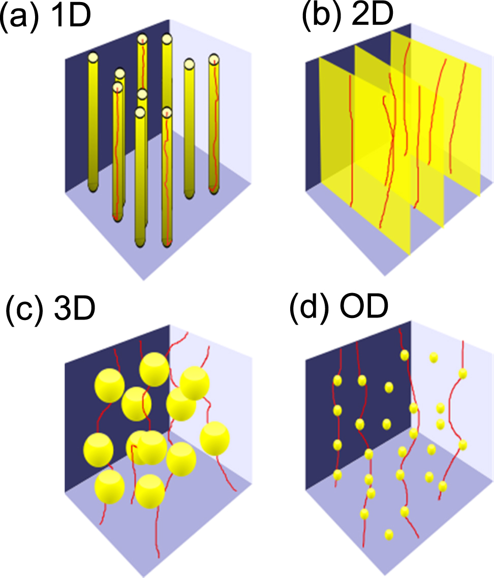
Furthermore, due to the very small length-scale over which the superconducting properties of REBCO can fluctuate (i.e. small coherence length, ξ) the range of defects that can pin vortices, known as artificial pinning centres (APCs), is immense. These entities include: dislocations, irradiation tracks (known as 1D pinning centres), stacking faults, antiphase boundaries, twin boundaries, grain boundaries, local in-plane misorientation surfaces (known as 2D pinning centres), voids and secondary phases (known as 3D pinning centres) [3]. It is also often assumed (although not explicitly verified) that even very small defects, smaller than ξ3, such as vacancies and substitutional atoms can act as pinning centres in REBCO [3], and this assumption is used in this review. These even very small defects are often identified as 0D pinning centres [9]. The four categories of defect are shown schematically in figure 1.

Figure 1. Illustrations of the different dimensional categories for defects. (a) 1D linear defects, (b) 2D planar defects (c) 3D large random defects (d) 0D point like defects (where defect sizes are ∼ξ3). In the online edition defect structures are in yellow and lines representing vortex cores are in red.
Download figure:
Standard image High-resolution imageThe overall effect of these multiple complications is that there is no definitive way to precisely predict Fp (and hence Jc) from a specific microstructure. However, thanks to over a decade of experimental work on optimising the pinning centre distribution and morphology, both in academia and in industry, huge progress has been made in the enhancement of Jc. There is also a range of theoretical studies (mostly on bulk REBCO) which have had a lot of success in explaining vortex behaviours under various experimental conditions [8, 10, 11]. Combined this large body of work has led to some general rules for linking particular pinning features to the Jc (T, B, θ) behaviour.
So far, the most successful strategy has been to add APCs via the creation of phases foreign to the RE–Ba–Cu–O system, known as secondary phases, through chemical additions to the REBCO starting composition before processing. The early examples of this are over a decade old, including [14] which reported how adding 5 mol% of BaZrO3 (BZO) to stoichiometric REBCO produced self-assembling nanoparticles of BZO within the REBCO matrix. BZO was chosen as it was known to be an excellent crucible material for growth of YBCO single crystals [12], mostly because it did not adversely react with the YBCO. Addition of BZO to REBCO films led to, with very little optimisation of the growth conditions, up to order of magnitude increase of Jc at liquid nitrogen temperature compared to un-doped films. Besides BZO there is now an extensive list of effective secondary phase APCs with BaHfO3 (BHO) [13, 14], BaSnO3(BSO) [15], Ba2YNbO6 (BYNO) [16–20], Ba2YTaO6 (BYTO) [21] and Ba2Y(Nb,Ta)O6 (BYNTO) [22–24], being the most widely explored.
To generate similar pinning enhancements, there has likewise been the use of non-stoichiometric RE:Ba:Cu ratios to develop 'intrinsic' non-superconducting secondary phases, such as RE2O3 [25], RE2Cu2O5 [26] and RE2BaCuO5 [27], often used in combination with the APCs mentioned above [28]. Other strategies to produce pinning centres have also been investigated, including decorating the substrates with particles to increase dislocation densities [29], using ion or neutron radiation [30–35] and, in another example of adjusting the chemistry, doping with multiple rare-earth elements (i.e. forming (Y, Gd, Nb, ...)Ba2Cu3O7−x [36]).
The focus of this review is how to utilize these strategies by understanding the chemical, thermodynamic and kinetic factors which enable different pinning centre sizes and distributions in REBCO to be designed to meet the many for different applications requirements. It is split into three sections. First, is a brief look at the microstructures which have been found to work well, i.e. the microstructures materials engineers should aim to produce. Second is a look at the kinetic and thermodynamic limitations that determine how and why such microstructures form, focusing specifically on PVD, to demonstrate what are the important design parameters. Third is a look at how combined chemical, kinetic and thermodynamic knowledge can be used to design optimised pinning centres in PVD CCs.
2. Optimised microstructures
2.1. Success criteria
The effectiveness of vortex pinning depends strongly on the microstructure and on the T, B operating conditions. This means that a particular microstructure will only be effective under a narrow set of conditions, and therefore a range differently pinned CCs must be made to fulfil the wide range of CC applications. It is therefore important to know how to engineer a wide range of microstructures for a particular processing route.
The major uses envisioned for CCs can essentially be split into two broad categories—power related and magnetic field generation. This has led to three general areas of focus: high-temperature/low-field, mid-temperature/mid-field and low-temperature/high-field as demonstrated in figure 2. The power related applications, including power cables and fault current limiters, are in the low-field region. Here, the only major magnetic field is the cable's self-field. High quality CCs have already been developed for the low field regime and commercial power transport products are already installed in electrical grids at various sites around the world, although cost is still a limiting factor. Applications in the higher field regions are almost all based on using CCs to produce (and thus be subjected to) strong magnetica fields. Mid to high field power applications include transformers, motors, generators, and superconducting magnetic energy storage. High-field magnetic applications include MRI, NMR, rotors etc [37]. All these applications and the temperature and field regimes they need to work are highlighted in figure 2 below. Today, low temperatures are needed for the CCs to have sufficiently strong pinning to meet the performance specifications. Hence, there is a trade-off between superior properties and increased operational cooling costs. This leads to the first of the main success criterion for CC—have as high a critical current as possible at as high a temperature as possible under the magnetic field strengths and orientation required for an application.

Figure 2. Operating magnetic fields and temperatures of various CC appliances based on data from [2]. Circled are the three general areas of focus: 1 = high-temperature/low-field, 2 = mid-temperature/mid-field, 3 = low-temperature/high-field.
Download figure:
Standard image High-resolution imageThe critical current in this criterion is a combination of Jc, the film width and the film thickness. Whilst it may appear an easy way to increase the critical current would be to increase the film thickness, it has often been found that Jc decreases as film thickness increases [3]. This has meant REBCO films have generally been limited to being less than 2 μm thick, and explains why most studies have tended to focus on increasing Jc (i.e. pinning) rather overall current and thickness.
The second success criterion for CCs is that they have as isotropic as possible Jc versus θ characteristics. Typically, the Jc peaks at certain θ angles which, although not completely detrimental, introduces an extra layer of complexity to the magnet design process. In a CC magnet, the windings are exposed to magnetic fields with various angles depending on the particular position in the winding. This means that each point of the CC will essentially have a different Jc (B) curve. It is then necessary to careful design the magnet to the specific anisotropic characteristics of the conductor in order to achieve acceptable performances and safety margins. Additionally, having isotropic wires would allow the many years of design and construction experience creating magnets with LTS conductors (e.g. the magnets used in current NMR and MRI magnets) to be utilised.
In fulfilling the two aforementioned criteria, hundreds of REBCO microstructures have been evaluated by research groups around the globe. Whilst fulfilling these criterion is yet to be achieved, with Jc's far below the theoretical (depairing) current density limit, and no PVD films fully achieving a truly isotropic angular response, there is now a large body of knowledge about the different APCs and morphologies that can be produced, and how they generally influence Jc at different B, T and θ. The fact that this is only a general idea is important here as, unfortunately, there are additional factors which make direct comparisons between research groups misleading [3]. This includes factors like the variety of reported characteristics (maximum pinning force, Jc (77 K SF) etc), the inability to compare the Jc's of films measured at different temperature and fields, and the oft-forgotten factors that can artificially inflate Jc (low film thickness, high substrate quality etc).
Nonetheless, useful information can be gleamed from looking at several of the best performing microstructures [6, 38–45] and the reasons given for why they work. A summary of some of these, broadly split into the three T and B regimes, is given in figure 3 and expanded in the sections below.

Figure 3. Schematic cross sections, and accompanying Jc versus  plots, for some of the best performing microstructures as a function of T and B. These are approximately split into the three sections highlighted in figure 2 (a) Region 1: a high-temperature/low-field regime with columnar APC microstructures, (b) Region 2: a mid-temperature/mid-field regime with a mixed microstructure and (c) Region 3: a low-temperature/high-field regime with a random isotropic defect microstructure, which turns from 3D defects (fine secondary phases or nanodots) to 0D defects (vacancies, atomic substitutions etc) as the temperature is lowered. The accompanying Jc versus
  curves for (a), (b) and (c) 0D regime microstructures used data from [46, 49] and [50] respectively. The Jc versus
  for the >5 T 3D regime in (c) is a schematic based on data measured at 3 T [51].
Download figure:
Standard image High-resolution image2.2. High-temperature/low-field regime
This regime covers 65–77 K and low to mid strength field (here defined as 0–1 T). The best performance (in terms of highest Jcs, highest irreversibility fields or highest flux pinning force densities) is achieved with microstructures which contain APCs of continuous columns of insulating secondary phases aligned parallel to c. Hence BZO [40, 42], BSO [46], BYTO [23] and BHO [14] all work well. The schematic of an ideal continuous column microstructure as well as a corresponding Jc versus θ plot from an actual columnar microstructure (with 25 wt% BSO added to YBCO) are shown in figure 3(a) and discussed below.
One of the critical parameters for the strength of a defect site is the volume (which for the linear vortices essentially means length) of vortex that the defect site traps. For a 0D defect this will be on the order of  For higher dimensional defects, it will be
  2L, where L is the trapped length [40]. As
  is small, the pinning potential for 0D defects is also small. At the relatively high temperatures of 65–77 K, there is enough thermal energy for vortices to escape any weak pinning potentials, making these weak pins inactive. Hence, at high temperatures only defects with a large volume and subsequently large pinning force are effective (for more detailed theoretical treatments please see [8, 11]).
Of these larger defects (i.e. 1D, 2D or 3D defects) columns offer the best trapped length per defect volume ratio. The maximum of this ratio occurs for a columnar defect, continuous from substrate to film surface, with a vortex (hence the external field) aligned along its length, and it has generally been found that the longer and straighter the columns are, the better the microstructure performs [46]. However, even when the columnar precipitates are just stacked atop one another in a pseudo 1D 'broken column'/or segmented structure they still offer exceptional performance near 77 K [47]. This is a result of the total pinning force on trapped vortices growing linearly with the total amount (i.e. length) of 1D defects, but only adding statistically for random 3D defects [8]. Moreover, the adjustment of the vortex system to its pinning landscape (i.e. the bending of the vortex to intersect the defects) which occurs for random defect pinning involves an additional energy cost [3].
When a REBCO superconductor is in a magnetic field oriented at an angle with respect to the orientation of the defect the vortices will also nominally tilt to this angle (although in reality the vortex may stay parallel to the defect up to a critical tilt [48]). In such a case, the vortex volume enclosed by the columnar defect will decrease to be only that of the intersection volume. This leads to the Jc versus  behaviour for this 'best' microstructure being very far from isotropic. A large peak in Jc occurs when the field is aligned along the defect, usually along c. This is often in addition to the intrinsic a/b plane Jc peak which is observed the field is parallel to the BaO/YO planes mentioned in section 1, as shown in figure 3(a).
Some attempts to get around the anisotropic angular Jc have been made. For example, theoretically more isotropic behaviour and a small enhancement in pinning strength was thought to occur for a microstructure of small columnar precipitates, broadly aligned with each other, but still having some splay in their orientation [48, 52, 53]. Such splayed column structures have been shown to have better performance than random particles [54]. However, they typically found to not outperform continuous columnar or 'broken column' microstructures [23].
It is also important to note that if the columnar density is high in a particular CC, there is still an appreciable volume of intersections with vortices. Thus, even when  0°, the pinning force is at least comparable and often higher than for films with no APCS. Thus, the pinning performance of columns, even though anisotropic, is still the superior morphology at 77 K.
Further optimisation can be achieved through optimising the size and density of the columns. In terms of optimising the column size, the maximum energy benefit arises from when columnar radius is around  as then the order parameter will have decayed to a low enough value at the centre of the column to generate a high pinning force. Further increases in the radius beyond this add little extra decay of the order parameter, and so little additional pinning force, which is why the optimal diameter columns are around this value [46]. However, it should be noted that a slight benefit may be found for larger columns when
  0° as the enclosed volume of vortex per defect will have increased. This is shown in [55] where having altered the diameter of BYNO columns in YBCO films by varying the deposition rate it was found that wider diameter columns produced wider B∣∣c peaks.
In terms of optimising the column density, consideration must be given to the intended field strength in use. For low field (<∼0.5 T) applications, the best microstructure has only the number of columns that just gives a one column per vortex arrangement, as this maximises the fraction of superconductor whilst maintaining the maximum pinning strength possible. In this region, optimizing a similar microstructure for a slighter larger field this can easily be achieved by increasing the density of columns (e.g. by increasing the mol% of dopant) to pin the larger number of vortices. However, eventually this stops working as increasing the volume fraction of APCs leads to a smaller volume of superconducting material [3, 56, 57]. This effect can be magnified by the creation of enhanced strain and increased (misfit) defect density in the regions around the APCs, both known to adversely affect superconducting properties [58]. The conflicting effects of increasing Jc due to more pinning and decreasing Jc due to a decreased superconducting volume fraction leads to the creation of an optimal APC fraction [40] usually around 10 mol% [56, 57].
A small caveat must be made for zero applied field i.e. when the tape is only under self-field [3]. In most cases, the best performance is achieved for microstructures with no secondary phases i.e. just perfectly crystalline REBCO [59]. Whilst there are some reports of higher Jcs for doped samples, e.g. [60] where for a BZO doped film Jc was roughly 40% larger than for an undoped film prepared under the same conditions, these conditions were optimised for BZO formation. A true comparison would need to compare the Jc of the BZO doped film with the Jc of a pure YBCO film deposited under conditions optimised for pure YBCO formation. This may have important implications for planned uses of CC for power transmission.
2.3. Low-temperature/high-field regime
As soon as research groups started to look at the lower-temperature/higher-field (here defined as 5 T and above) regime, it soon became apparent that the microstructures that produced the best Jc performance were not the same as the best microstructure at 77 K [40, 61] operation. This was paralleled by similar results which studied Jc versus  characteristics, where it was found that microstructures giving reasonably isotropic behaviour at 77 K were more anisotropic by 30 K [51]. At low temperatures, where there is less thermal energy, even weak pins are active. Combined with the decreased
  and
and  (respectively from ∼5 nm and ∼0.7 nm at 77 K to ∼2 nm and ∼0.3 nm at 10 K in pristine YBCO) this allows even atomic sized defects, like vacancies and substitutional atoms, to act effective as pinning centres. This leads to the type of pinning defect which dominates the total pinning strength changing from the anisotropic columnar shaped particles to various smaller isotropic defects [50] as shown schematically in figure 3(c). This often leads to Jc versus
  curves that are flat bar the intrinsic a/b plane peak, as shown in figure 3(c). This also explains phenomena like the disappearance of a discernible B∣∣c peak [61] and broadening of the B∣∣a/b peak [40] in BZO doped REBCO tapes when the temperature is lowered from 77 to 30 K.
Models describing how the pinning changes to being dominated by isotropic defects as the temperature is lowered split the isotropic defects into two categories roughly correlated with size: (1) strong pinning centres like small precipitates, stacking faults when field aligned parallel to them, etc, which become effective at moderately low temperatures (<∼50 K); and (2) weak pinning centres around  in size like vacancies, substitutional atoms etc, which rapidly dominate pinning at the lowest temperatures (<∼10 K).
The rise in the effectiveness of these pinning centres as the temperature is decreased has been shown to approximately follow the exponential relations:


where  (0) is the strong pinning contribution to Jc at 0 K,
  (0) is the weak pinning contribution to Jc at 0 K and T+/T− are the corresponding characteristic temperatures of vortex pinning at strong and weak defects respectively.
A clarifying example of how the contribution of each type of pinning centre can change with temperature, in this case for a pure YBCO film deposited by trifluoroacetate metal organic deposition, is given in figure 4, based on data from [50]. Whilst these equations are phenomenological and are not expected to work for every case, they do have some justification in various theoretical models [50]. It is important to note that the anisotropic columnar defects which are so important at high temperatures are still active. Indeed, they still offer the strongest pinning per defect when the core of the vortex is aligned along it. Yet the relative contribution of this pinning site to the total pinning strength has decreased. The main cause of this phenomenon is the fact that the small weak defects will exist at much higher densities than the larger stronger defects. As the total pinning force for a particular type of defect will depend in some way on the number of such defects, once the weaker pins become active at lower temperatures [50], the sheer number of them means they simply swamp the effect of the columnar defects.

Figure 4. Temperature dependence of the current density contributions from strong anisotropic (here stacking faults), strong isotropic and weak isotropic pinning centres for a YBCO sample formed by CSD based on data from [50].
Download figure:
Standard image High-resolution imageThis is not to say that APCs are useless at lower temperatures. Studies such as [51, 61] have shown that the critical current values for BZO doped samples are still higher than undoped samples, even at lower temperatures. This is because the strong pinning contribution can still make up a non-negligible fraction of the total pinning force [50]. Not only this, but adding secondary phases can induce the creation of additional weak and strong pins (such as stacking faults and vacancies) to relieve the misfit strain around the precipitates. This explains why there is a new optimal secondary phase distribution and morphology at lower temperatures. The best performing microstructures are not just those with a few columns but are now those which have a secondary phase distribution which maximises the number of small defects and disorder in the REBCO lattice (something which was detrimental at 77 K).
One way to realise this goal of maximising disorder can be met by increasing the secondary phase volume to much higher levels than is typical at 77 K. Studies where this has been done (up to 50 mol% of BZO [62]) have produced very good results. Another method excepted to work in theory is moving the microstructure away from long columnar precipitates to one with a high density of fine spherical shaped nanodots (i.e. very fine 3D type defects). The spherical shape creates more strain in the REBCO lattice than columns do (see section 3.3 below), whilst the high density of nanodots means there is less room for this strain to relax between precipitates [63]. This should then generate a large amount of additional 0D point defects and 1D misfit dislocations as the lattice attempts to relieve the large strain. Just such superior performance was recently reported in a study that compared samples with reasonably fine spherical Y2O3 nanoparticles with samples containing columnar BZO particles [64].
The change from the dominant pinning factor being columnar defects at high temperatures to being multiple small defects at lower temperatures has the additional advantage of making the pinning more isotropic. With these defects distributed almost randomly and in such high numbers throughout the microstructure a vortex will feel a strong interaction no matter its tilt relative to the axis of the a/b plane or the orientation of the APCs.
2.4. Mid-temperature/mid-field regime
The mid-T/mid-field regime is ill-defined and covers a much broader range than the regimes discussed above. Here, it is broadly defined as 1–5 T, covering any application that will have fields of a few Tesla where the benefits to Jc of additional cooling below 77 K are likely to offset the increased cooling costs. The Jc in this higher field region is also often found to follow a Jc  B−α law, creating a new parameter to compare and identify the best microstructures (with a smaller α meaning a better performing conductor).
The best microstructure is this region is no longer just a microstructure with a maximised amount of disorder/number of weak pinning sites. This is because the temperature is too high for weak pinning sites to be active. This field range is also too high for an effective one-column-per-vortex microstructure to be built. This is not because you cannot create a columnar defect density high enough (in [62] the inter-BZO spacing is only 10 nm for a matching field of 21 T) but because doing so would generate a high level of lattice disorder in REBCO and thereby dramatically reduce Tc.
Instead within the mid-temperature/mid-field region the best performing samples are those with mixed microstructures [65–67]. A mixed microstructure can be described as columnar 1D rods (usually broken up into segments) interspersed with smaller 3D discs or 3D spherical nanoparticles, usually of a different phase to the 1D rods. A schematic example of this mixed microstructure is shown in figure 3(b). This type of microstructure has been produced multiple times, sometimes deliberately e.g. when an excess of both Zr and Y was added to create columnar BZO with Y2O3 nanoparticles [66–68], and sometimes unexpectedly 'self-forming' in films where only one secondary phase was deliberately added (e.g. BYNO to form columns) but another secondary phase (e.g. spherical Y2O3) formed as well [22, 24, 65].
The creation of smaller precipitates, like RE2O3, YBa2Cu4O8 and CuxO, being catalysed by the formation of the main columnar precipitates is often seen in PVD films [69]. It occurs due to the strain field around the columns lowering the nucleation energy for the new secondary phase and via the local composition change around the columns as certain elements are used up to form it [70].
When analysing why mixed microstructures demonstrate superior performance the surprising result is that it is not just due to a simple superposition of the anisotropic columnar pinning and isotropic smaller phase pinning. In fact, it has repeatedly been shown that the addition of different defect types does not lead to the sum of the properties of the APCs on their own [66]. In the mixed microstructure case a synergic effect occurs, where the smaller phases inhibit a low activation energy method for vortex movement between the columnar defects. As shown in figure 5, vortices can move between columns without depinning the entire vortex at once [66, 71]. Instead, they can do so by depinning only small sections to form loops or bubbles. Under a Lorentz force these bubbles will swell, incurring only a small energy cost due to the small extension to the vortex length, which allows part of the vortex to intersect an adjacent linear defect to form a kink. Once this kink has been created the remainder of the vortex can transfer, via the movement of the kink arms, to the new columnar defect with no extra energy cost [72] as the length of un-pinned vortex never exceeds the length of the kink arms. Thus, the activation energy to transfer has been reduced from depinning the entire vortex length to only the small section of the kink arms, much like the passage of a dislocation allows for shear at much lower stresses than would be required for the simultaneous shift of an entire plane of atoms. However, when another smaller precipitate is put between the columns the expanding kink becomes repinned, preventing the rest of the vortex translating to the new column.

Figure 5. (a) Growth of a vortex bubble due to the Lorentz force FL. (b) Low energy cost method of transferring of a vortex between two columnar pinning centres via movement of kink arms. (c) Stopping kink arm movement due to additional pinning centres with pinning force Fp.
Download figure:
Standard image High-resolution imageThe mixed microstructure also has the benefit of a more isotropic angular Jc behaviour compared to microstructures with just plate or column shaped APCs [69]. For instance, the actual Jc versus  plot in figure 3(b), from a YBCO sample with BHO columns intermixed between Y2O3 plates, shows strong pinning at all angles and relatively small
  = 0° and
  = 90° peaks. Additionally, this benefit generally gets better as the temperature is lowered [40].
The temperature is in fact a key part of why the mixed microstructure becomes the most effective microstructure. This is because in this mid-temperature region the temperature is too high for weak 0D pins to be active. Hence stronger 3D pinning sites, such as the small precipitates found between the columnar precipitates, are needed. Furthermore, because of the presence of columnar and random precipitates, there is a relatively high secondary phase volume fraction and hence also level of disorder (such as oxygen vacancies etc) in the REBCO matrix which often reduces the Tc [58].
3. Understanding secondary phase formation
3.1. Factors which influence secondary phase self-assembly
The phase separation and self-assembly of nanoprecipitates in the REBCO matrix during PVD processing is governed by kinetic and thermodynamic factors. Included in the thermodynamic considerations are strain and the growth of epitaxial factors which are additional features in the growth of epitaxial REBCO films compared to the growth of bulk REBCO. These arise from both interface and volume effects. Interface strains arise due to the lattice mismatch between the secondary phase and REBCO matrix, e.g. ≈8% between BZO and REBCO phases [73]. This strain is relieved by the creation of misfit dislocations, and falls to zero when enough dislocations are formed so that the interface becomes incoherent, although the energy cost associated with the creation of these dislocations allows particles to remain coherent to relatively large sizes. The case is slightly different in CSD where the pre-formed secondary phase particles not only have incoherent interfaces with the REBCO but also induce strain-related defects in the nearby REBCO matrix [74].
Volume strains arise due to the mismatch between the volume created for a precipitate in the matrix and the volume the precipitate phase would naturally take up, a result of the differences in density between the precipitate and the matrix.
Overall the interplay of kinetic and thermodynamic factors in epitaxial films means that the secondary phases which form are often not those found in bulk REBCO crystals. Furthermore, whilst the driving force to minimise strain will promote certain particle morphologies, the kinetic constraints can prevent these shapes from forming.
3.2. Columnar pinning centres
Columnar shaped secondary phases can occur as continuous columns, but they also frequently occur as shorter cylindrical shaped rods. These short rods can be arranged randomly or stacked atop one another, which is known as the 'broken column', segmented or bamboo structure. Many of the APC's currently used in PVD are found to form columnar shapes during deposition, including BZO [73], BSO [46], Ba2RENbO6 [17], Ba2RETaO6 [21]. This is largely due to the very tight kinetic constraints in effect during film formation.
As with any secondary phase formation the first step is nucleation. This requires the phase to reach a critical radius size r*. The number of nucleation events that occur, and the number of these that reach r* will set the final number of precipitates. Once the particle has reached r* it will continue to grow outwards until it becomes buried by newly deposited material. This effectively limits the secondary phase to only be able to grow 'up' as bulk diffusion is dramatically slower than surface diffusion [75] and gives a kinetic explanation for why columns, as opposed to plates, begin to form.
If limited time for particle growth alone was responsible for the final particle shape, then the radius should simply be set by a  term (where D is the diffusion coefficient of the rate limiting species and t is diffusion time) and the mol% of dopant. This is because
  is the radius of the disc-shaped diffusion field around each nucleation event, within which species could diffuse to the nuclei in the time available before it is buried, and the mol% sets how many species there will be within that diffusion field. Increasing either of these would lead to more atoms reaching the nuclei, and so to a larger final particle radius. Indeed, decreasing t (by increasing the repetition rate in a PLD deposition) or decreasing T (hence D) has been report to lead to smaller radii [55, 76]. However, above a certain threshold, the radius does not change as the mol% is increased [77]. Instead the same sized columns, just at a higher density, are found.
The fact the columnar radius is independent of the mol% suggests that there is also a strain effect which sets the radius. This arises as the particles nucleate epitaxially in the matrix, and then maintain this epitaxy as they grow, creating the misfit strain (and accompanying energy cost) discussed above. The strain scales with the interfacial area but is not perfectly localised to interfaces and stretches some volume into the REBCO matrix. This provides a weak driving force for spatial ordering and an 'equilibrium' columnar radius as this minimises the energy cost (i.e. level of strain in the REBCO) relative to a random pattern [63]. In fact detailed models of this phenomenon, at least for low volume density of secondary phase particles, have shown that the strain field generated by the coherent interface layers of secondary phase, film and substrate is the dominant driving force for the self-organisation of the nanostructures and that the self-assembly of columns only occurs when the secondary phase has the correct mismatch and elastic constants [77, 78].
Additionally, although the strain–energy cost would preferentially lead to the creation of continuous columns (as this minimises the total phase boundary area), the short time for diffusion also means that formation of the next layer of the secondary phase is not guaranteed, and instead the column can become truncated and covered by layers of REBCO. Future nucleation events of the secondary phase in the REBCO then become most likely in the strain fields above the nanocolumns [63] leading to the precipitates to growing in the previously mentioned bamboo structure [70]. The length of the nanorods that form is therefore very susceptible to the growth conditions such as temperature and presence of other secondary phases [79].
3.3. Plate shaped pinning centres
If the kinetics do not completely dominate other precipitates shapes can form. One of the most commonly found is the plate shape. Plates are able to form when the kinetics, or rather the diffusion rate, is no longer limiting. This can be due to an abundance of the elements that form the precipitate being present when the particle forms. This is the case for inherent secondary phases, e.g. RE2O3, and when a high mol.% of the APC components are used [62, 69]. It can also occur by simply adjusting the processing conditions, such as raising the substrate temperature (which increases D) or by lowering the repetition rate (increasing t) [69].
Why plates often represent the lowest energy morphology is a question with multiple answers. One of the most widely given is the minimisation of total interfacial energy. This applies in the case of a precipitate with many surfaces that have coherent interfaces to the matrix, but one of which has a much lower interfacial energy cost per area than the rest. The precipitate then grows so that the large area 'face' of the plate is formed of the low energy interface, whilst the higher energy interfaces are relegated to the smaller area 'sides' of the plate.
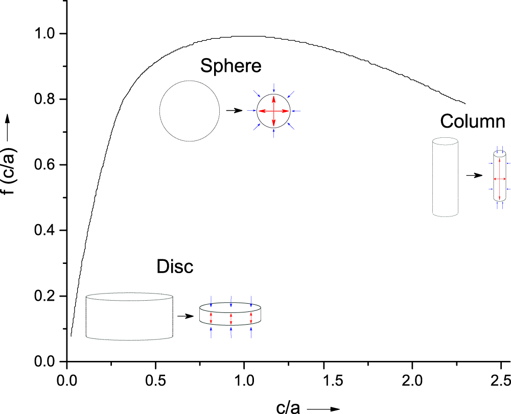
The plate shape can also form to minimise volume strain. The volume strain in the matrix and precipitate is not isotropic when the secondary phase shape is non-spherical. This means that the total strain energy changes with precipitate shape. For a homogeneous inclusion in an incompressible matrix this change in strain energy per volume is given by:

where μ is the shear modulus, Δ the volume misfit, f(c/a) is the shape factor with typical values of 1011 N m−2, 3% and 0–1 (unitless) respectively giving strain energy values of 100–500 J cm−3 [80]. This is plotted in figure 6 and clearly shows that the strain energy is lower for plates than for columns or spheres [81]. When an elastically anisotropic precipitate and matrix are considered, as they should be for REBCO, plate formation becomes even more favourable. This is because for plate shaped precipitates the strain generated in the matrix normal to the large face of the plate is much smaller than at the sides. The overall strain energy can therefore be further decreased if a plate is formed with the normal to its large face parallel to the matrix's stiffest direction.

Figure 6. Change in shape factor (and therefore misfit volume strain energy) with ellipsoid c/a ratio (i.e. shape) based on data from [66]. Inserts are schematics showing the generation of volume strain in the three distinct precipitate shapes.
Download figure:
Standard image High-resolution imageA final method to induce plates is to disrupt the strain fields that led to columnar self-assembly. This can be achieved using vicinal substrates where, above a threshold vicinal angle, the interplay between the new substrate-YBCO interface strain fields and secondary phase-YBCO interface strain fields can lead to the secondary phase forming as plates [82].
3.4. Spherical pinning centres
The last precipitate shape that is frequently found to form is one which is roughly spherical. This occurs when the interfacial energy is high over all interfaces (such as for incoherent precipitates) to the extent that it outweighs any volume strain minimising effects. In this case, the shape that forms is driven to minimise its surface area to volume ratio i.e. form a sphere.
Spherical particles are mostly seen when the secondary phase forms before the REBCO. While well documented for metal-organic deposition (MOD) and chemical solution deposition (CSD) this can also occur in PVD processes e.g. reactive co-evaporation by deposition and reaction (RCE-DR). RCE-DR is a process where the starting materials is first put down as an amorphous layer, heated until partially liquid and finally crystallised as REBCO by a rapid methods of processing the pO2 [83]. The growth mechanisms involved are very similar to other liquid assisted growth methods of processing REBCO [84, 85]. Spherical RE2O3 particles form in the 'melted' amorphous pre-layer [86] but remain in the final film. In all of MOD, CSD and RCE-DR, the pre-formed phases will bear no crystallographic relation to the REBCO as they nucleated randomly in a pre-layer, whilst REBCO grows with a fixed biaxial texture set by the substrate. Incoherent interfaces then form as the fast formation rate does not allow time for the diffusing species to find a low energy arrangement.
4. Engineering and designing pinning centres
4.1. Choosing chemistry for secondary phase formation
4.1.1. Limiting factors
The choice of elemental additions that can be doped into REBCO seems at first to encompass any element on the periodic table. If only a small amount of an element is added then it will remain in solid solution within the REBCO matrix, being substitutional if big and interstitial if small. With a greater level of addition a new secondary phase may form within the REBCO matrix. Whether this secondary phase will work as an effective pinning centre depends on two factors, the level of solute in the REBCO matrix in equilibrium with the precipitate phase and whether it can form in the kinetically demanding processing conditions.
4.1.2. Equilibrium solute level for artificial secondary phases
The level of solute in the REBCO matrix in equilibrium with the precipitate phase is important as most solute atoms will 'poison' the REBCO (i.e. dramatically worsen its superconductor properties) when present at a high enough concentration [41, 87]. This has limited the effectiveness of many APCs. For instance, both SiO2 [88] and Al2O3 [89] have been tried as pinning centres in (bulk) REBCO. Although some Jc enhancement was achieved, because the concentration of Si and Al in YBCO in equilibrium with a given volume fraction of SiO2 or Al2O3 was high, only a tiny volume fraction of secondary phase could be put in before the poisoning effect dominated. This limits the Jc improvement to much less than is achievable with a conventional APCs like BZO. Hence, to be effective, a secondary phase should either comprise of elements intrinsic to REBCO (e.g. made of benign rare-earths Nd, Sm, Eu etc [3]) or it should comprise of elements with extremely low equilibrium solute concentrations.
Unfortunately, trying to predict a precise equilibrium concentration of solute requires intricate modelling and great computing power, but again some general remarks can be made. Foremost, the solute level depends on the relative difference between entropy (essentially how many places the solute atom can go) and enthalpy (essentially strength of the bonding) of the solute atom in the REBCO lattice and in the secondary phase. This is why interstitial elements such as C and N (hence carbide and nitride APCs) should be avoided. The large number of interstitial sites in REBCO creates a large entropic force for C and N to enter into the matrix i.e. a high equilibrium solute content. This is also why having a substitutional solute ion with a widely different ionic radius to RE, Ba or Cu is beneficial; the steric strain cost detracts from the bonding enthalpy reducing the driving force of the solute ion to dissolve in the matrix.
The stable oxidation state of the dopant ion also plays a role in determining equilibrium solute concentration of an ion. If a solute element with a usual oxidation state of 1+ is to replace a lattice atom of oxidation state 4+ the bonding strength is reduced, either due to the smaller effective charge 1+ or due to the high cost of nominally oxidising the ion to a 4+ state. Furthermore, a solute atom usually in a 5+ state will be unstable in a structure where it would nominally have a 3+ charge. Instead it would be preferential for the 5+ ion to form a secondary phase in which it can maintain its 5+ state. In this manner, we can explain the success of BZO, BHO, BSO, BYNO and BYTO, i.e. precipitation after doping with Zr, Hf, Sn (oxidation state +4) and Nb, Ta (oxidation state 5+). These oxidation states are much higher than the ions in YBCO (nominally 2 + or 3+) which leads them to prefer to form new phases in which they can keep their higher oxidation state rather than remain as substitutional defects.
4.1.3. Intrinsic secondary phases
An alternative pinning option is to use intrinsic secondary phases (single and mixed oxides of RE, Ba and Cu) to improve the pinning properties of CC tapes [64]. The great advantage here is it is impossible to poison the REBCO lattice. One of the most common and most powerful intrinsic secondary phases is RE2O3. RE2O3 can be formed by adding excess RE under the right processing conditions [64]. RE2O3, as well as any number of other intrinsic secondary phases, can also form in large numbers in REBCO if it is doped with the correct primary APC as mentioned in section 2.4.
4.2. Why perovskite APCs?
4.2.1. Coherency
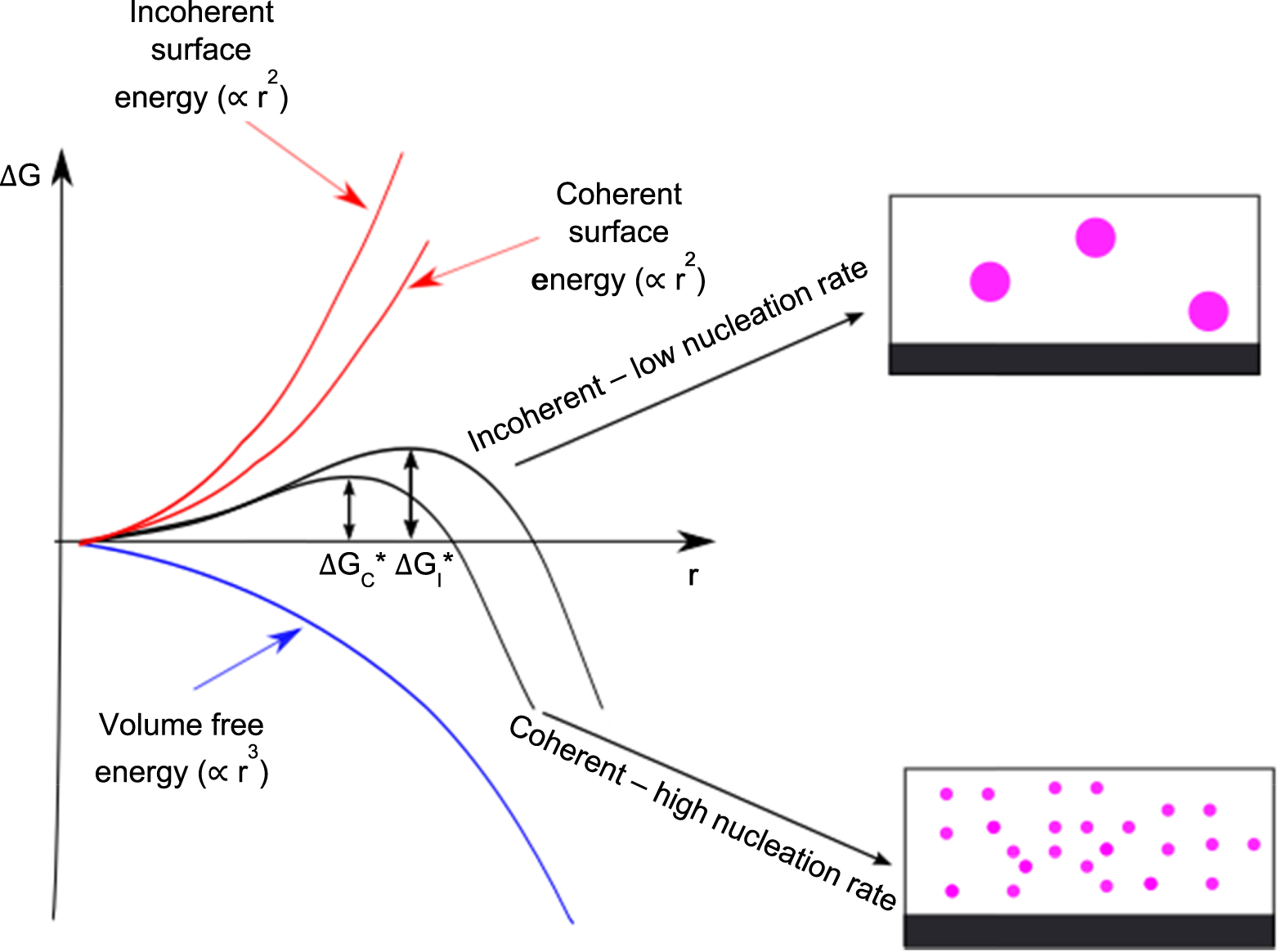
As mentioned above, phase formation in PVD is often severely kinetically limited. This can mean that secondary phases which should be present for thermodynamic reasons can be supressed. Instead, a highly disordered supersaturated REBCO lattice may result. To avoid forming such a far-from-equilibrium supersaturated REBCO with poor superconducting properties and to instead promote secondary phase formation, the nucleation rate of the APC must be fast enough such that multiple nucleation events can occur in the limited time available for atomic motion during deposition. Whilst this does depend on many factors e.g. the substrate temperature, oxygen pressure, species arrival rate etc, one of the biggest contributions is the interfacial energy between the REBCO matrix and secondary phase.
From elementary nucleation theory [81, 90] we expect a nucleation rate of the form

with

where Rn = nucleation rate (events m−3 s−1), ΔG* = activation energy (kJ mol−1), C = magnitude factor related to the number of possible nucleation sites (positions m−3), f = frequency factor related to atomic vibration (s−1), γ = interfacial energy (mJ m−2) and ΔGv = free energy change per volume on forming new phase (mJ m−3) [81]. There is a wide range of possible values for these physical quantities, varying in many orders of magnitude, due to the large variety of contributing factors e.g. temperature, composition or whether precipitation is in a perfect crystal or region with a high concentration of defects. However, due to this exponential dependence on γ3, having a low interfacial energy is always a key factor in determining how fast a phase forms (as shown in figure 7) and so whether it will be kinetically supressed. This is why most secondary phases which form at the same time as REBCO in CCs have coherent interfaces with it (or occasionally the substrate).

Figure 7. Schematic figure demonstrating the competing effects of volume free energy and surface energy cost that lead to equation (4.2). ΔG, r, ΔGC*, ΔGI* are the volume free energy change, radius of APC nucleus and activation energy to nucleate particles with coherent and incoherent interfaces respectively. Also shown is the change in ΔGC* due to an increasing surface energy cost (e.g. due to incoherent interfaces) and its effect on the nucleation rate.
Download figure:
Standard image High-resolution imageIt is possible to generate APCs with coherent interfaces by carefully choosing the chemistry and thus APC phase which forms. Coherent interfaces are most likely to form when both the lattice parameters and the crystal structures of the two phases are close. The crystal structure and lattice parameters of REBCO are shown in figure 8(a) and its unit cell is best described as being built from a stack of three perovskite-like subcells, with its lattice type being either tetragonal or orthorhombic depending on the oxygen content. This means that to have a good chance of coherency, APC phases are mostly restricted to either a single perovskite (figure 8(b)) or double perovskite (figure 8(c)).

Figure 8. Crystal structures of (a) REBCO, e.g. YBa2Cu3O7−x (YBCO); (b) single perovskite ABO3, e.g. BaZrO3 (BZO); and (c) double perovskite A2BB'O6, e.g. Ba2YNbO6 (BYNO).
Download figure:
Standard image High-resolution imageFortunately adapting the chemistry to create single perovskites or double perovskites is simple. Single perovskites have the form ABO3 with a charge distribution A2+, B4+ and O2−. On the other hand, double perovskites have a A2BB'O6 form with a charge distribution A2+, B3+, B'5+, and O2−.
When aiming to form APC perovskites, single or double, in REBCO, the A site cation must have 2+ valence. This essentially restricts the ion to barium as the other 2+ ions (with similar ionic radii) will, owing to the identical oxidation state, sit at the Ba site in REBCO with little energy cost. This in turn means a detrimentally high concentration of the 2+ ion will remain in solid solution in the REBCO lattice before there is driving force big enough to form a precipitate. A similar effect restricts the B site ion in the double perovskite to be a rare-earth element.
This leaves the only variable for determining which APC will be formed as which B' site ion. Charge balance dictates that if a 4+ ion (B'4+) is chosen, then a single perovskite will form, whilst if a 5+ ion (B'5+) is chosen a double perovskite will form. The only constraint on which 4+ or 5+ ion can be used is that the ionic radius must lie within a certain range, so the perovskite structure that forms will have a similar enough lattice parameter to REBCO to form a coherent interface with it. This leads to the most common B site ion choice being those highlighted in figure 9 below.

Figure 9. Periodic table with the elements that have the best oxidation states and ionic radii to form artificial pinning centres highlighted. Coloured boxes indicate B site cations commonly used in perovskite APCs when doped into REBCO. Red boxes highlight the B cations which form single perovskites and blue boxes highlight the B cations which form double perovskites.
Download figure:
Standard image High-resolution image
Even within perovskite APCs, there are varying degrees of coherency. Interfaces with larger misfits create more misfit dislocations [46], which, because they are additional strong pining centres, can increase Jc. However, if the misfit is too large, this raises the interfacial energy too much and undermines the point of having coherent interfaces at all. Furthermore, increased misfit means secondary phase nucleation events are less likely to occur within the REBCO grains (as desired for the best pinning effect) and instead they will concentrate at grain boundaries where the nucleation activation energy is decreased [89]. Also, having a reduced misfit may bring additional benefits if the CC is to be used at 77 K. This arises as a smaller misfit typically means less REBCO c expansion and subsequently less depression of the Tc. For example, in [69], YBCO films were doped with either BHO or BYNTO. The resulting elongation in c and drop in Tc was smaller for BYNTO (11.74 Å, 91.0 K) than BHO (11.76 Å, 87.5 K). Reduced misfit should also lead to thinner columns and higher densities of columns, as a smaller lattice strain leads to a smaller equilibrium radii.
4.2.2. Incoherency
If we relax the condition that the secondary phase needs to form at the same time as the REBCO, we can get microstructures that include incoherent particles. This is the case for growth processes such as RCE-DR or CSD. Incoherent particles can introduce advantages. For instance, around the incoherent particles in REBCO films and CCs made using CSD, high levels of strain is produced in the (usually softer) surrounding lattice [91]. This in turn results in the generation of defects such as stacking faults, intergrowths and plane buckling [50, 91] which act as strong pinning APCs across a wide T range. Moreover, as coherency is no longer a requirement, the choice of secondary phase is larger and includes non-perovskite phases. However, producing such microstructures usually requires the secondary phase to be preformed [92–94] which restricts the deposition options to only a few deposition methods, Oswald ripening (coarsening) and interdiffusion of the APC elements into the REBCO matrix can result at high growth temperatures, which puts more limitations on the APC choice.
4.3. Designing defects
4.3.1. Designing perovskite APCs
As shown in figure 3, for the high-temperature/low-field regime, e.g. for applications such as cables and fault current limiters, long continuous columns are desired, whilst at lower temperatures shorter, finer APCs are desired. As discussed in section 3.2 there are both kinetic and thermodynamic factors which influence whether a APC will grow as continuous columns, bamboo structures or random nanodots. This makes trying to predict the microstructures that will form for different APCs challenging. However, some broad predictions are possible, especially in cases where one effect dominates.
For example, it is possible to predict that continuous columns will form if the ions forming the APC perovskite have a fast diffusion rate, so that the APC growth will not be overtaken by the simultaneously growing REBCO lattice. Generally speaking, the diffusivity of dopant atoms in oxides increases as the melting point of its binary oxide decreases [55]. This means that long straighter columns are more likely to form when the binary oxides of the dopant ion in the APCs has as low a melting point as possible. This explains why BSO forms continuous columns in REBCO under deposition conditions where BZO columns become segmented, begin to bend and eventually splay [46]. While both BSO and BZO have similar levels of mismatch to the YBCO lattice, and so similar strain/thermodynamic driving forces to form columns, the much lower melting point of SnO2 compared to ZrO2 (1630 °C and 2715 °C respectively) means Sn4+ had a much higher diffusivity than Zr4+ during growth.
As already mentioned, for lower-temperature/high-field applications, finer, more random (and hence isotropic) defects are desired. The easiest way to proceed to these isotropic defects is to increasing the APC nucleation rate by increasing the volume fraction of precipitate used, or by adjusting the processing conditions, e.g. increasing the repetition rate in PLD [55, 75]. Another way to produce finer APCs is to form APCs with complicated structures as, in crude terms, more complicated structures have slower growth rates. For instance, using a double perovskite with mixed B'-site cations, i.e. doping with Ta and Nb in BYNTO as opposed to only Ta or Nb, leads to nanocolumns of only 30 nm in length under conditions where the BYNO and BYTO form columns over 100 nm in length [65].
To further refine the particle size to be as small as possible, it is important to consider that the radius of columnar particles is fixed at an equilibrium value which is set by the coherency strain. The radius will generally get larger when the coherency strain is larger because a larger misfit means a higher effective interfacial energy, thus create a larger driving force to reduce the total interface area, and, for a fixed volume fraction of precipitate, there is less area for fewer wider columns than many fine ones. In this way, BSO has a larger radius than BZO [46] and BYNO has a larger radius than BYTO [65], when deposited under the same conditions.
4.3.2. Engineering other defects for the low-temperature/high-field
Besides forming small perovskite APCs, other possible small isotropic defects for the low-temperature/high-field regime are intrinsic secondary phases or point (0D) defects.
Considering first intrinsic secondary phases, e.g. RE2O3, the formation of very small particles (∼ in size and so quasi-0D) is made difficult by the abundance of the constituent elements of the intrinsic phase in the matrix as this means they tend to coarsen during the later stages of processing, although it can be done by very careful control of processing [95]. However, as mentioned in section 2.4, it is also possible to form intrinsic secondary phases via a primary APCs (henceforth called secondary-effect particles), due to the solute depletion and strain fields the primary APC produces. The sensitivity of these secondary-effect particles to chemistry is exemplified by comparing BYTO and BYNTO APCs grown under the same processing conditions. Here either no additional secondary-effect nanoparticles are formed (as is the case for BYTO), or a range of tiny YBa2Cu4O8−x (Y124) and Y2Ba4Cu7O15−x (Y247) type structures dispersed between slightly larger Y2O3 nanoparticles are formed between the primary APC columns (BYNTO) [23]. The fact that APCs can be used to create secondary-effect particles opens up a much wider variety of processing methods that can be used to create tapes with quasi-0D pinning centres compared to relying on those methods which need to directly form the intrinsic phase.
It is important to note that the wrong choice of primary APC can lead to adverse effects. For instance in [69] films doped with Hf (to form BHO) had a large decrease in the number of smaller intrinsic Y2O3 compared to undoped YBCO when grown under the same conditions. It is also true that not all smaller phases are useful. In [40] it was found that Cu2O plates formed in BZO-doped YBCO under certain Y:Ba:Cu ratios, but these plates detrimentally interrupted the BZO growth, leading to worse Jc characteristics than films with only BZO columns.
At present, there is no single dominating factor which can be pinpointed to predict the details of secondary-effect phase formation. However, a starting point for making a high density of very fine secondary-effect phases is to first produce a high density of very fine APCs, as this maximises the strain in the REBCO lattice, thus helping to drive secondary-effect particle formation. The kinetics and thermodynamics of the APC formation is again critical, as for the other temperature and field regimes already discussed. Whilst careful tuning of very fine APC structures and has been shown in [62, 75], more studies are needed in this area, especially in the low-temperature/high-field regime where such small secondary-effect particles will be most effective.
Finally, we consider the 0D random defects e.g. vacancies and atomic substitutions, which can either form around APCs or in the REBCO lattice. Such 0D defects are much more like true point defects compared to the quais-0D secondary-effect particle defects discussed above, but like the secondary-effect particles they form in larger numbers around APCs due to the coherency strain fields. 0D defects can also be made to form in the REBCO lattice by using mixtures of multiple rare-earths to form the REBCO i.e. (RE,RE')BCO. This occurs as size mismatch effects from both RE mixing and small-RE/Ba cross-substitution [3, 36] create localised strain fields in the REBCO lattice. This, as well as the localised electron depletion zones also produced by cross-substitution, act as vortex pinning sites. In particular, Sm and Ba cross-substitution has been shown to be marginally beneficial to pinning at 77 K [36, 96]. Again the effect of this defect inducing strategy at low temperatures, where it is likely to be most effective, has not been widely explored and is certainly worthy of much more detailed study.
4.4. Adapting material chemistry for faster processing
As the high cost of CCs is widely credited as the biggest barrier to CC use [63] there is a growing drive to find new production methods with a faster throughput. Choosing the right chemistry for the REBCO CC and APC is crucial for enabling crystalline REBCO formation at very high rates (and hence tighter kinetic constraints) while also giving desired APC morphologies and distributions.
For PLD, a faster repetition rate is an obvious way to force faster REBCO growth. For this to be successful the APCs must also be able to form fast. This requires APCs containing fast diffusing ions to overcome the problem of not enough species arriving at nucleation events to let them reach r* in the shorter time available for diffusion. For instance, it was shown that using Nb doping to form BYNO allowed columnar precipitates to form under conditions where Zr doping to form BZO did not [55]. This occurs even though the strain mismatch between the precipitates and YBCO (7.6% and 8.4% for BZO and BYNO respectively), and thus nucleation activation energy and r*, are similar for both APCs, demonstrating the benefit of choosing fast diffusing component ions [55].
Even faster REBCO formation rates can be achieved if the RE:Ba:Cu ratio is altered to produce a liquid phase at the processing temperatures. In this case, the deposition method is known as a liquid-assisted processing. The great advantage of having a liquid during processing is the faster species diffusion, for instance the diffusivity of Y at 970 °C in liquid YBCO and solid YBCO is 4 × 10⁻¹⁰ m2 s−1 [97] and 8 × 10⁻¹² m2 s−1 [98] respectively, i.e. over 100 times faster. This allows both the REBCO and any APCs to form much quicker than in other methods.
One of the best examples of a liquid assisted process is the RCE-DR process discussed above. A liquid phase develops when a deposited amorphous phase decomposes allowing for the rapid conversion to REBCO (<30s [54]). This, combined with the fast rate of deposition, means RCE-DR holds the record for CC throughput per hour (360 m h−1) for an industrial CC process [83]. Here the main pinning centres are intrinsic RE2O3 nanoparticles which are formed as a consequence of the off-stoichiometry nature and fast reaction route used with this method.
When using liquid assisted methods controlling the RE:Ba:Cu stoichiometry presents new pinning engineering options. Changes to this ratio influences the volume fraction of the film that is liquid, thus the diffusion speed, whilst the REBCO is forming. This can have big effects on the final microstructure, changing not only secondary particle size but also affecting their distribution. As an example in [54], a study which used the RCE-DR method, changes to the RE:Ba:Cu ratio changed the arrangement of the Gd2O3 particles from small nanoparticles stacked parallel to c for films with low liquid volume fractions during REBCO formation, to larger randomly arranged particles for higher liquid contents. This new way to control the rate of diffusion, by choosing the fraction of liquid present during film formation, could lead to novel microstructures in the future. Success in this area will enable us to achieve the ultimate goal of high production volumes of low cost, high-performance conductors. However relatively little research has been done in this area so far.
5. Conclusion and outlook
We have come a long way since the first CC was made and now a large body of work on the best pinning strategies at different fields and temperatures is available. Similarly, there is a lot of established knowledge on the secondary phase microstructures that form with different chemistries and processing conditions. Hence, the coated conductor community has a general guide about how, with appropriate chemistry and processing, a range of microstructures can be achieved that work well under certain B, T and  conditions. However, since until quite recently the main focus was on pinning optimisation at 77 K, one regime where knowledge is still far from complete is the low temperature (<30 K), high field regime.
This paper has addressed the basic materials science knowledge for enabling design and engineering of a wide range of pinning centres for the broad application specifications; all the way from 77 K, low field applications, to <30 K, high field applications. For the less studied but increasingly important low-temperature/high-field regime new challenges lie ahead. First among these is developing reliable new methods to identify the sub-nanometre (i.e. effectively 0D) defects which dominate the pinning strength at low temperatures. Many research groups have found that identifying such tiny defects and tiny particles in TEM is hard [70], even when the number of defects is high enough to generate indirect evidence via Jc versus  curves [50]. This is especially true when there is such a high level of disorder in the REBCO lattice (as desired for the low T regime) that individual defects become hard to identify [91]. Further challenges also lie ahead in the development rapid rate, low cost, CC production. Here, a better understanding of the increased dominance of kinetic factors is needed to ensure successful design and engineering of pinning centres. If all these challenges can be met the dream of widespread high temperature superconductors for a range of power and magnetic applications will be one step closer.
Acknowledgments
This work was supported by the Engineering and Physical Sciences Research Council, Doctoral training account (grant number EP/N509620/1), EUROTAPES, a collaborative project funded by the European Commission's Seventh Framework Program under Grant Agreement No. 280432, and also partially funded by SuNAM Co., Ltd, and Applied Materials, Inc.