

Abstract
Metal-insulator-semiconductor (MIS) structures were fabricated by depositing an Al2O3 dielectric on top of the contact layer of a mid-wave infrared nBn detector based on n-Hg1-xCdxTe grown by molecular beam epitaxy on GaAs (013) substrates. It is shown that when creating a backward electrode on the absorbing layer, the form of the capacitance–voltage characteristics depends not only on the properties of the contact layer, but also on the properties of the barrier and absorbing layers. An equivalent circuit of MIS structure based on nBn detector with mesa configuration is proposed. It is shown that measurements of the admittance of MIS structures with mesa configuration allow one to study the properties of the barrier layer in the nBn structure. The influence of infrared radiation on the temperature dependence of the barrier layer resistance is studied.
Export citation and abstract BibTeX RIS
1. Introduction
Important modern tasks are increasing the operating temperature and improving the manufacturability of highly sensitive infrared detectors based on mercury cadmium telluride (HgCdTe) [1, 2]. Therefore, the development of nBn detectors based on HgCdTe grown by molecular beam epitaxy (MBE) is promising. With this architecture of detectors, it is possible to suppress some components of the dark current (surface leakage and Shockley–Reed generation current) [3]. In addition, when creating detectors, the defect-forming operation of ion implantation [4], which is usually used to form pn junctions in hybrid photodiode arrays based on MBE HgCdTe [2], can be excluded.
Since the creation of the concept of nBn detectors [5], the greatest successes have been achieved with the creation of such detectors based on materials of group III–V [6–10], which is associated with favorable band offset at heterointerfaces. The outstanding fundamental properties of HgCdTe stimulate research into the possibility of creating highly sensitive nBn detectors based on this material. Theoretical studies are conducted in various scientific groups [11–15], but only a small number of works are known devoted to the practical implementation of nBn structures based on MBE HgCdTe [16–18].
Recently, the creation of MWIR nBn structures based on MBE HgCdTe with Al2O3 passivation was reported, for which a diffusion-limited dark current was observed in the temperature range 180–300 K [19, 20]. The optimization of the parameters of nBn structures is impossible without a detailed study of the processes in multilayer unipolar structures based on HgCdTe MBE Thus, measurements of admittance revealed a number of differences between nBn structures based on MBE HgCdTe [21, 22] and structures based on III–V [23–25], which, for example, consist in high-temperature distortions due to surface states at heterointerfaces. Additional information may be provided by studies of the electrical characteristics of metal–insulator–semiconductor (MIS) structures created by depositing a dielectric on top of an nBn structure. Earlier studies of the admittance of specially fabricated MIS devices based on III–V barrier structures for determining the dopant concentration in the barrier layer were reported [23]. The use of MIS structures for studying processes in nBn structures based on MBE HgCdTe provides the possibility of obtaining information on the properties of the contact layer [26], as well as using a whole range of techniques [27–29].
This paper presents the results of studies of the admittance of test MIS devices created by applying a dielectric on top of the contact layer of nBn structures based on HgCdTe MBE MIS devices were created in planar and mesa configurations in which a backward electrode was formed on the contact layer and the absorbing layer, respectively.
2. Experimental details
Heteroepitaxial HgCdTe films were grown by molecular beam epitaxy [30, 31] at the Rzhanov Institute of Semiconductor Physics, Siberian Branch of the Russian Academy of Sciences. On top of the GaAs (013) substrate, 50 nm and 5 μm thick buffer layers of ZnTe and CdTe were formed, respectively. Between the CdTe buffer layer and the HgCdTe absorbing layer, a graded-gap HgCdTe layer was grown in which the composition at the distance of 1 μm varied from 0.63 to 0.29. The composition in the absorbing layer (x = 0.29) corresponded to the boundary wavelength of 4.87 μm at the temperature of 200 K. This composition provided the possibility of intrinsic absorption in the MWIR spectral range. The epitaxial growth rate was 1.50 μm h−1. The thickness of the absorbing layer was 2.52 μm. The composition in the 120 nm thick barrier layer was 0.67. When growing the barrier layer, the cadmium flux increased due to the complete opening of the Cd source shutter. The composition in the contact layer with the thickness of 350 nm was 0.33. During the growth process, an indium donor impurity was introduced into HgCdTe film using the source of In molecular flux. Based on the selected technological regimes, the indium concentration in contact, barrier and absorbing layers was 3.8 × 1015 cm−3. All layers of the active region of the nBn structure had an electronic type of conductivity (n-HgCdTe). Figure 1(a) shows the layout of the layers in the grown epitaxial film.
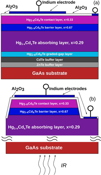
Figure 1. Schematic illustration of the arrangement of layers in the fabricated MIS structure in (a) planar (sample A) and (b) mesa (sample B) configuration.
Download figure:
Standard image High-resolution imageIn the fabrication of device nBn structures [19–22], the HgCdTe film is etched to an absorbing layer for the subsequent formation of contact frame. Then the HgCdTe film is etched in 0.5% solution of Br in HBr to form a mesa configuration. After that, about 90 nm thick Al2O3 dielectric film is deposited using a plasma-enhanced atomic layer deposition (PE ALD) [32–34]. The dielectric is applied at the sufficiently low temperature (120 °C), which prevented mercury evaporation from HgCdTe film in vacuum [34]. To create a front contact to the nBn structure, the PE ALD Al2O3 layer is then etched using a mixture of hydrofluoric acid and ammonium fluoride. Electrodes are formed by thermal spraying at temperatures not exceeding 100 °C.
When creating test MIS devices based on nBn structures, two different configurations were used. When creating type A samples (planar configuration, figure 1(a)), etching was not performed to form the mesa structure and the standard contact frame was the return electrode. Also, etching was not performed to ensure contact with the nBn structure, and the front indium electrode with the area of 1.34 × 10⁻³ cm–2 was deposited on top of the PE ALD Al2O3 dielectric layer. When creating type B samples (mesa configuration, figure 1(b)), etching to the absorbing layer was carried out to form mesa structure. The backward contact for samples B was a contact frame, which was also performed as for nBn structures. For samples B, the front indium electrodes with an area of 4.91 × 10⁻⁴ cm–2 were also deposited on top of the Al2O3 dielectric.
Admittance measurements were performed using an automated setup based on the Agilent E4980A immittance meter, Janis non-optic cryostat and LakeShore temperature controller. The setup provided measurements in a wide range of temperatures (8–300 K), frequencies (1–2000 kHz) and voltages (from −30 V to 30 V). A bias voltage was applied to the front (top) indium electrode relative to the backward contact, which was grounded. In the forward direction of the voltage sweep (FVS), the bias voltage changed from negative values to positive values, and in the reverse direction of the voltage sweep (RVS), the bias voltage changed from positive values to negative values. Equivalent schemes of MIS structures and formulas for calculating the differential resistance of the space charge region (SCR) are given, for example, in [35, 36].
3. Results and discussion
Figure 2(a) shows the capacitance–voltage (C–V) characteristics of MIS structures with the planar configuration (sample A), measured at the frequency of 10 kHz at various temperatures for forward and reverse voltage sweeps. In measurements, a parallel equivalent circuit was used (inset). The low-frequency behavior of the C–V characteristics of MIS structures is realized if the concentration of minority charge carriers in the inversion layer manages to follow the change in the alternating test voltage [27]. In this case, the capacitance of the MIS structure in the strong inversion mode is close to the capacitance in the accumulation mode and is determined by the dielectric parameters. With the high-frequency behavior of the C–V curves, the carrier concentration in the inversion layer does not have time to change when the test voltage changes. Then the capacitance of the MIS structure in strong inversion mode is constant and minimal, and the value of this capacitance depends on the dopant concentration. Figure 2(a) shows that at the frequency of 10 kHz, the C–V characteristics show a high-frequency behavior at the temperature of 9 K and a low-frequency behavior at the temperature of 300 K. It was previously shown that the hysteresis of the observed type is associated with the recharging of slow states in the transition layer between the dielectric and the semiconductor [37, 38]. The capacitance of the MIS structure in the accumulation mode, which is close to the dielectric capacitance, is practically independent of temperature. The density of slow surface states at the flat band voltage can be determined by the formula:  where CD is the dielectric capacitance, ΔV is the voltage shift of the C–V characteristics for forward and reverse voltage sweeps for the flat band capacitance, q is the electron charge, A is the area of the field electrode. For sample A, the density of slow states is close to 1011 cm–2. The flat band capacitances were calculated taking into account dopant concentration values determined by the MIS structure capacitances in the strong inversion mode. Figure 2(b) shows the corresponding C–V curves of MIS structures with a mesa configuration (sample B). Figure 2(b) shows that at the frequency of 10 kHz, capacitive dependences at the temperature of 9 K show an almost high-frequency behavior, and at the temperature of 300 K—a low-frequency behavior. The hysteresis is more pronounced and the density of states for sample B is close to 4 × 1011 cm−2. For sample B, an unusual temperature dependence of the capacitance of the MIS structure in accumulation is observed: at the temperature of 300 K, this capacitance is approximately 2 times greater than at 9 K.
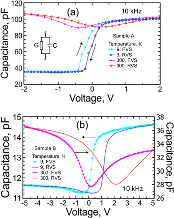
Figure 2. C–V curves for MIS devices (a) A and (b) B, measured at the frequency of 10 kHz at various temperatures with forward and reverse voltage sweeps.
Download figure:
Standard image High-resolution imageFigure 3(a) shows the C–V characteristics of a planar MIS structure (sample A), measured at different frequencies at the temperature of 210 K with a forward voltage sweep. It is seen that with an increase in the frequency from 2 to 50 kHz, a transition from low-frequency to high-frequency behavior is observed. Figure 3(b) shows that for the MIS structure in the mesa configuration, the high-frequency behavior of C–V curves in the frequency range from 50 to 1000 kHz is not observed even at the much lower temperature (77 K).
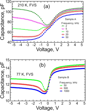
Figure 3. C–V curves for MIS devices (a) A and (b) B, measured at different frequencies for forward voltage sweep at the temperatures of 210 and 77 K, respectively.
Download figure:
Standard image High-resolution imageThe transition of the C–V characteristics from low-frequency to high-frequency behavior is determined by the value of the differential resistance of the SCR in the strong inversion mode [26]. The value of the differential resistance is determined by the generation rate of minority charge carriers in the near-surface semiconductor layer. This generation rate for MBE HgCdTe depends on the concentration of defects in the near-surface layer of the semiconductor, through the levels of which generation processes can pass. Figure 3 shows that the value of the differential resistance of the SCR should be much larger for the MIS structure with planar configuration (sample A).
Figure 4 shows the temperature dependences of the capacitance measured at the frequency of 10 kHz for samples A and B in the modes of accumulation and strong inversion. For the planar MIS structure (sample A), the accumulation capacitance slightly increases upon heating from 9 to 300 K, which is associated with the temperature dependence of the dielectric constant of Al2O3 film. Significant increase in the capacitance for this sample in the temperature range 150–250 K is associated with the transition from high-frequency behavior to low-frequency behavior.
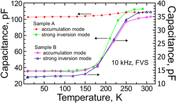
Figure 4. Temperature dependences of the capacitance of MIS devices in the accumulation and strong inversion modes for samples (a) A and (b) B, measured at the frequency of 10 kHz.
Download figure:
Standard image High-resolution imageFor MIS structures with mesa configuration of the capacitance, in the accumulation and strong inversion modes, they increase significantly in the temperature range 150–270 K. This type of temperature dependence of the capacitance in accumulation is unusual and cannot be explained by the temperature dependence of the dielectric constant.
Figure 5(a) shows the experimental dependences of the capacitance and normalized conductance on frequency for a MIS device with mesa configuration (sample B) measured at the temperature of 250 K and forward voltage sweep. The normalized conductivity is  where ω is the angular frequency,
  is the conductance of the MIS structure when it is presented in the form of a parallel RC chain. Figure 5(a) shows that the frequency dependencies cannot be explained only by the influence of the series resistance of the semiconductor bulk (as for sample A). To simulate the frequency dependencies, an equivalent circuit was used, which is shown in the inset. In this equivalent circuit, CD is the dielectric capacitance of Al2O3, RB and CB are the resistance and capacitance of the barrier layer, and Rbulk is the series resistance of the bulk of the absorbing layer. In order to obtain expressions for the capacitance and conductance of the MIS structure, one can replace the parallel chain (RB–CB) with the serial chain (RBS and CBS) according to the formulas:
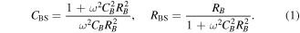
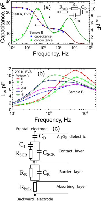
Figure 5. (a) Experimental (symbols) and calculated (lines) dependences of the capacitance and normalized conductance on frequency at the temperature of 250 K in the accumulation mode; (b) experimental dependences of the normalized conductance on frequency at the temperature of 290 K and various bias voltages for the MIS structure with mesa configuration (sample B) and (c) equivalent circuit for MIS structure with mesa configuration in inversion mode.
Download figure:
Standard image High-resolution imageIf you imagine the MIS structure in the form of series-connected capacitance CS and resistance RS, then you can write:

Then you can convert the serial chain to parallel by the formulas:

In explicit form, the relationship of the elements of the equivalent circuit with the measured values of capacitance and conductance can be described by the following relationships:
From the measured experimental dependences of the capacitance and conductance on the frequency in accumulation mode, it is easy to determine the values of all elements of the equivalent circuit. The capacitance of the MIS structure at low frequencies is close to the capacitance of the CD; the value of the barrier capacitance CB strongly affects the capacitance C in the 'shelf' section in the frequency range 200–1000 kHz. The resistance value RB can be found by the position of the low-frequency maximum of the normalized conductance, and the resistance values of Rbulk by the high-frequency decay of the capacitance or the high-frequency maximum of the normalized conductance. The calculated dependences are close to the experimental dependences (figure 5(a)) for the following values of the elements of the equivalent circuit: CD = 34.5 pF, RB = 58.6 kOhm, CB = 26.1 pF, Rbulk = 2.2 kOhm.
The equivalent circuit shown in the inset to figure 5(a) is valid for accumulation mode. It is important that the values of the capacitance and resistance of the barrier layer, as well as the bulk resistance, are independent of the applied voltage. Since the thickness of the contact layer exceeds the maximum width of the SCR, the obtained values of RB and CB characterize the properties of the barrier at zero voltage across the barrier.
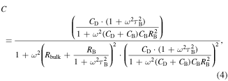
Figure 5(b) shows the experimental dependences of the normalized conductance on frequency for the sample B, measured at the temperature of 290 K and various voltages. Figure 5(b) shows that when biased from the accumulation mode to the strong inversion mode, the conductance maximum appears at lower frequencies. For the inversion mode the equivalent circuit is shown in figure 5(c), where CI is the inversion layer capacitance, CSCR and RSCR are the capacitance and resistance of the SCR, respectively. Surface states that may be present in nBn structures at heterointerfaces [21] do not appear in measurements of admittance at the selected voltages. Therefore, RC-elements characterizing surface states are not included in the equivalent circuit used for the calculation. SCR is located in the contact layer near the interface between HgCdTe and the Al2O3 dielectric. In the MIS device under study, a small voltage drops on the nBn structure itself; therefore, the influence of the depletion regions near the barrier layer on the admittance can be neglected.
Having determined the values of the elements of the equivalent circuit in the accumulation mode, one can find the values of the parallel connected capacitance and conductance of the MIS structure (CMIS and GMIS) at any bias voltage, eliminating the influence of the barrier layer and the resistance of the absorbing layer.
Given the expressions (1)–(3), we can write:

where RP and CP are the series-connected resistance and capacitance of the MIS structure, which are equal:


where  G and C are the measured values of the conductance and capacitance of the MIS structure at an arbitrary bias voltage using a parallel equivalent circuit.
Figure 6 shows the C–V characteristics for the MIS structure with a mesa configuration (sample B) measured at different temperatures at a frequency of 100 kHz, and also the corresponding capacitive dependencies after eliminating the influence on the measured values of the resistance and capacitance of the barrier layer, as well as the absorbing layer resistance. After processing the experimental C–V curves, it is possible to determine the main parameters of the MIS structures (dopant concentration and differential resistance of the SCR).
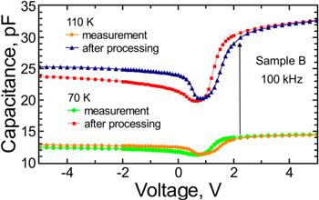
Figure 6. C–V curves for MIS device (sample B), measured at frequency of 100 kHz for forward voltage sweep at temperatures of 70 and 110 K and the corresponding C–V curves after processing the experimental dependences using formulas (6)–(8).
Download figure:
Standard image High-resolution imageThe ionized dopant concentration (Nd) can be found using the following formulas [26]:
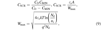
where CMIN is the minimum high-frequency capacitance of a MIS structure in strong inversion mode, Wmax is the maximum equilibrium width of the SCR, which is realized in strong inversion mode, ni is the intrinsic concentration, εs is the dielectric constant of the semiconductor, k is the Boltzmann constant, T is the temperature.
For the MIS structure with planar configuration (sample A), the dopant concentration determined from capacitive measurements was about 3.6 × 1015 cm–3, which is close to the concentration of indium impurity. For the MIS structure with mesa configuration (sample B), the concentration of the dopant was higher (about 1.6 × 1016 cm–3). The reasons for the increase in dopant concentration remain debatable and require additional research. To characterize the generation rate of minority charge carriers in the surface layer of a semiconductor, the value of the product of the resistance of the SCR in the strong inversion mode by structure area (RSCRA) is used [35, 36]. For sample A, the RSCRA value reaches 1.4 × 10⁵ Ohm × cm2, which is significantly larger than the value of this parameter for sample B (6.3 × 10² Ohm × cm2). Despite the fact that etching can cause changes in the electrical properties of the near-surface HgCdTe layer [39–42], the determination of the reasons for the difference in the parameters of the A and B structures remains debatable. A possible cause of this difference may also be defect formation due to Al2O3 deposition for surface passivation.
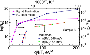
The admittance measurements of MIS devices based on nBn structures can be used to study the properties of the barrier layer. Figure 7 shows the temperature dependence of the resistance of the barrier layer in the dark mode and under illumination. It can be seen that, upon cooling, the RB values increase, and illumination by radiation with a wavelength of 0.94 μm limits this resistance at low temperatures. Figure 7 shows the Arrhenius plots in the dark mode, which show two linear sections with the activation energies of 346 and 16.5 meV. At low temperatures (10–30 K), deviations of the experimental points from a linear dependence are observed, which may be associated with a decrease in the accuracy of determining the barrier resistances due to the very large values of these resistances.
Figure 7. Temperature dependences of the barrier resistance in the dark mode and under illumination for the MIS structure with mesa configuration (sample B), as well as Arrhenius plots in the dark mode.
Download figure:
Standard image High-resolution image
The above activation energies should be prematurely compared with the defect energies in HgCdTe, since the accuracy of this new technique has not yet been studied. It is most likely that at high temperatures the barrier resistance is limited by the Shockley–Read generation processes. Additional studies are needed to elucidate the mechanism of formation of low-temperature activation energy. It can be noted that for a more rigorous interpretation of the results shown in figure 7, it is necessary to take into account the temperature dependence of the energy gap in barrier layer of the nBn structure [2]. The capacitance of CB is practically independent of temperature, since it is determined by the geometric parameters of the fully depleted barrier layer. The resistance of the absorbing layer increases by about 3 times when heated from 10 to 200 K, which can be explained by the temperature dependence of the electron mobility. When heated from 200 to 300 K, the role of holes in the total conductivity of the absorbing layer increases, which leads to a decrease in Rbulk.
4. Conclusions
Thus, test MIS structures were fabricated by depositing an PE ALD Al2O3 dielectric on top of the contact layer of the nBn structure based on MBE HgCdTe. Parameters of the nBn structure are suitable for detecting mid-wave infrared radiation. Test MIS structures were fabricated in planar and mesa configurations, with the backward electrode deposited on the contact and absorbing layers, respectively. Admittance measurements of test MIS structures showed that for a structure with mesa configuration, a pronounced temperature dependence of the capacitance in accumulation and a lower frequency form of the C–V characteristics are observed than for structures with planar configuration.
It was found that for the MIS structure with mesa configuration, the capacitive characteristics depend on the properties of the barrier layer. Using the method of equivalent schemes, expressions are obtained that make it possible to exclude the influence of the barrier parameters and absorbing layers on the measured C–V characteristics. It is shown that the admittance measurements of fabricated test MIS structures can be used to study the properties of the barrier layer in nBn structures. From the temperature dependence of the barrier resistance, the activation energies are determined, which are 16.4 and 346 meV at different temperatures.
Acknowledgments
The work was supported by the Russian Science Foundation (Grant No. 19-12-00135).