
Abstract
Semiconductor nanowire (NW) quantum devices offer a promising path for the pursuit and investigation of topologically-protected quantum states, and superconducting and spin-based qubits that can be controlled using electric fields. Theoretical investigations into the impact of disorder on the attainment of dependable topological states in semiconducting nanowires with large spin–orbit coupling and g-factor highlight the critical need for improvements in both growth processes and nanofabrication techniques. In this work, we used a hybrid lithography tool for both the high-resolution thermal scanning probe lithography and high-throughput direct laser writing of quantum devices based on thin InSb nanowires with contact spacing of 200 nm. Electrical characterization demonstrates quasi-ballistic transport. The methodology outlined in this study has the potential to reduce the impact of disorder caused by fabrication processes in quantum devices based on 1D semiconductors.
Export citation and abstract BibTeX RIS

Original content from this work may be used under the terms of the Creative Commons Attribution 4.0 licence. Any further distribution of this work must maintain attribution to the author(s) and the title of the work, journal citation and DOI.
Introduction
Low-dimensional semiconductors are of significant importance for the development of quantum technologies. For example, InSb and InAs NWs show a diverse range of appealing characteristics, such as strong spin–orbit coupling (SOC) [1] and substantial g-factors of up to ∼50 [2, 3]. These properties make them optimal candidates for the realization of topological qubits based on Majorana zero modes (MZMs) [4–7] and of spin–orbit qubits [8–10]. In addition, these materials can interface well with superconductors, enabling electrostatically-tunable gatemon-type superconducting qubits [11–13]. In general, the development of such devices requires precise nanopatterning and the integration of dissimilar materials, such as superconductors or other metals and insulators, with the NWs.
Recent theoretical works [14, 15] suggest that disorder plays a significant role in obscuring topological features in MZM devices, and ultimately prevents their reliable observation. Disorder can arise from growth, but even in pristine materials it can be induced during the device nanofabrication process. Therefore, complementary to improvements in synthesis, optimizing the device nanofabrication and suppressing the effects of fabrication-induced disorder are key requirements for the creation of robust quantum states in devices based on NWs and other low-dimensional semiconductors.
Nanomanufacturing techniques play a crucial role in the fabrication of quantum devices with low-dimensional semiconductors. Top-down methods like photolithography, electron beam lithography (EBL) [16], and ion beam lithography [17], are commonly employed. However, recent observations suggest that these methods may induce structural damage or introduce resist contamination in low-dimensional materials, further complicating the fabrication of high-performance electronic devices [18–20].
Among these techniques, EBL stands out as a widely used and reliable method for metal electrode patterning at the nanoscale [21]. This method creates precise patterns using a high-acceleration electron beam (e-beam) on electron-sensitive resist, achieving nanometric resolutions. However, the high acceleration voltage that is required to achieve such resolution might cause charge traps in the dielectric and damage the semiconductor [22, 23]. EBL also requires high vacuum conditions and lacks facile in situ imaging capabilities due to the complexity and cost associated with multi-beam systems. Another limitation of EBL arises from the need of implementing proximity effect correction methods to mitigate unintended exposure of the resist in areas not directly targeted by the e-beam [24]. While attempts have been made to improve the NW growth process and the dielectric environment [25, 26], alternatives to EBL have received relatively little attention.
Recently, a reduction of overall contact resistance and enhancement of the performance of field effect transistors (FET) was achieved in monolayer MoS2 by using thermal scanning probe lithography (t-SPL) instead of e-beam lithography [16], suggesting that the t-SPL prevents damaging the semiconductor material while exposing the pattern, which is desirable for semiconducting NW based quantum devices.
Thermal scanning probe lithography (t-SPL), uses a heatable ultra-sharp tip for the simultaneous writing and reading of nanoscale structures on thermally-responsive surfaces, namely on thermal resists [27, 28]. The t-SPL cantilever integrates a thermal height sensor and a heating element, both instrumental in the fabrication of nanoelectronics, and quantum computing devices [29]. Additionally, the t-SPL tip can be used for in situ thermal nanoimaging during the patterning, allowing for the inspection of the quality of the written features without the need for separate metrology instruments. For writing, the heatable ultra-sharp tip is scanned over a sample surface, inducing localized changes through thermal stimulation, which results in patterns with sub-20 nm features. To increase the throughput of the high-resolution thermal probe and make it more suitable for applications that require microscale and millimeter-scale features, we exploited the capabilities of the integrated laser writer in the hybrid lithography tool. The laser writer head uses a continuous wave (CW) laser with an emission wavelength of 405 nm for the residual-free direct laser sublimation (DLS) of thermal resists and the creation of larger-area structures (>500 nm).
In this work we patterned quantum devices based on ∼65 nm wide InSb NW using a mix and match lithographic approach combining both t-SPL and direct laser writing in a single commercial hybrid lithography instrument. This setup enables us to achieve high resolution through t-SPL, and high throughput via direct laser writing, utilizing the same tool, the same resist stack, and the same thermal decomposition process of the resist layer. The contact spacing between source and drain electrodes, set to ∼200 nm to achieve quasi-ballistic transport, was patterned using the thermal probe. The vias and the bonding pads were patterned using the laser writer head to reduce the overall patterning time. We show using magneto-conductance measurements at low temperatures that transport in the resulting device can be mediated by a small number of quantum modes upon suitable electrostatic gating.
Experimental
InSb NWs with ∼65 nm diameter were grown using the vapor liquid solid (VLS) technique. The growth process is described in detail in [26]. The NWs were deterministically transferred from the growth substrate to a local Ti/Au back gate covered with ∼40 nm of ALD-grown AlOx using a dedicated transfer station (see schematic description in figure 1(a)). A bilayer resist stack consisting of 250 nm of Poly(methylmethacrylate- co- methacrylic acid) (PMMA co MA, i.e. PMMA/MA) as underlayer and 55 nm of Polyphthalaldehyde (PPA) as top layer was spin coated over the substrate.
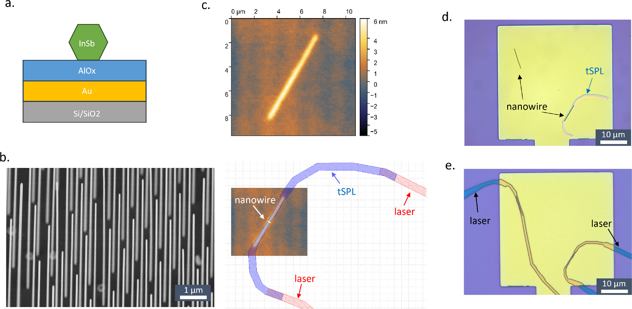
Figure 1. (a) Schematic showing a cross-section of the substrate used, with the NW and the metallic top gate separated by an oxide layer. (b) SEM image of the InSb NW growth chip. (c) Topography reading (top) of the nanowire buried under the resist stack, generated in situ via thermal nanoimaging. The image of the nanowire is then use as a reference for the markerless overlay of t-SPL fine electrode lines (bottom). The part of the electrodes that will be patterned by the t-SPL and laser are shown in blue and red, respectively. (d) Optical microscope of the sample after the t-SPL, upper image, and after the laser writing, lower image (e), after the DLS step.
Download figure:
Standard image High-resolution imageThe device patterning took place in a NanoFrazor Explore (Heidelberg Instruments Nano AG), equipped with a thermal scanning probe for the writing of nanometric features i.e. the source drain electrodes that are ∼200 nm apart, and a laser writer head that utilizes direct laser sublimation (DLS) to create the larger contact features, such as the pads and vias to the leads. Before initiating the electrode patterning process, the InSb nanowire is imaged in situ beneath the resist stack using the tip in cold mode similarly to conventional atomic force microscopy. Existing topographical features in a sample are detected on the topography reading of the resist layer coated on the sample surface [30]. This thermal nanoimaging technique is damage-free and allows for the in situ generation of topography images, hence avoiding the need to expose the sample to an e-beam or to move it to a separate metrology tool for inspection. The residual topography of the nanowire buried under the polymer stack is detected with great accuracy, with lateral resolutions of less than 10 nm and sub-nm vertical resolution.
Once the topography image is generated, it can be used as a reference for overlaying the electrode patterns with an alignment error of less than 5 nm, without the need for additional alignment markers on the sample [27] figure 1(b) shows in situ topography image of the InSb NW coated with the resist stack and the pattern overlay for t-SPL. The NW appears wider, ∼1  compared to ∼65 nm shown in the SEM image, as a result of flattening of the wire topography and softening of its edges due to the height of the resist stack. After spin-coating the two resist layers, the initially flat resist surface develops a residual topography amplitude, which is vertically aligned with the nanowire underneath [30]. From the resulting image, we measured a residual topography of approximately 4.5 nm, which allows for easy detection and precise markerless overlay on the nanowire.
Next, we initiated the patterning process by delineating the high-resolution sections of the source and drain electrodes through t-SPL. The remaining components of the device architecture, including the electrode fan-outs and 200 μm × 200 μm electrode pads, were then written using direct laser writing. The fine features produced by t-SPL cover an area of roughly 20 μm × 20 μm and were patterned within a span of 5 min. On the other hand, the electrode fan-outs and contact pads, measuring approximately 700 μm × 1200 μm, were written using the laser writer head in a time frame of 45 min. Consequently, the entire writing process for the NW device required less than 1 h to complete. In this hybrid lithography setup, the laser writing as well as the t-SPL patterning use the same positioning system, and the lateral offset between the two is automatically calibrated via the tool's software. To the best of our knowledge, there have not been reports of complete device writing using solely the mix and match of lithography techniques, namely, no reports of millimeter-large area electrode patterning using DLS.
Similar to the thermal probe, the laser beam utilized initiates thermal decomposition of the PPA layer, causing it to sublimate immediately without redepositing on the sample. This reaction, which is residual-free, endothermic, and devoid of damage to the underlying sample and nanowire, eliminates the need for subsequent chemical development to pattern the PPA. The layer can then serve as a mechanically stable etching mask for the underlying PMMA/MA organic transfer layer. Subsequently, we begin the PMMA/MA chemical wet etching process to transfer the patterns written in PPA and achieve an undercut. A solution consisting of 5 vol% deionized water (DIW) in isopropanol (IPA) is employed to ensure a controlled PMMA/MA etch rate of 1 nm s−1. The pattern creation and transfer process is shown in details in the Supplementary data.
The wet etching process in diluted isopropanol (IPA) reveals the NW under the bilayer resist stack within five minutes. Before the subsequent contact metallization step, it is necessary to remove the native oxide from the NW. The native oxide was removed from the InSb NW using an argon (Ar) ion milling step. Then, the metallic contacts (10 nm of titanium and 120 nm of gold) were deposited in an Ultra High Vacuum deposition system with in situ Ar ion milling capabilities. The patterned devices were measured in a dilution refrigerator at base temperature of ∼10 mK using standard lock-in techniques.
Results and discussion
Figure 2(a) shows the patterned PPA after t-SPL process. The gold square is the Au/AlOx back gate with the lead to the bonding pad. The metallic gate is coated with a ∼40 nm conformal layer of atomic layer deposition (ALD) grown AlOx. The small leads were patterned using the t-SPL and the vias that connect them to the bonding pad were patterned using DLS. A topography map that was obtained using the thermal scanning probe is shown in figure 2(c). This map shows that the regions patterned by both techniques (t-SPL and DLS) have well-defined lateral boundaries. The t-SPL-patterned region is ∼70 nm deep, while the laser-patterned one is ∼90 nm deep, which indicates that for both pattering techniques the nanowire was protected by the PMMA/MA resist.
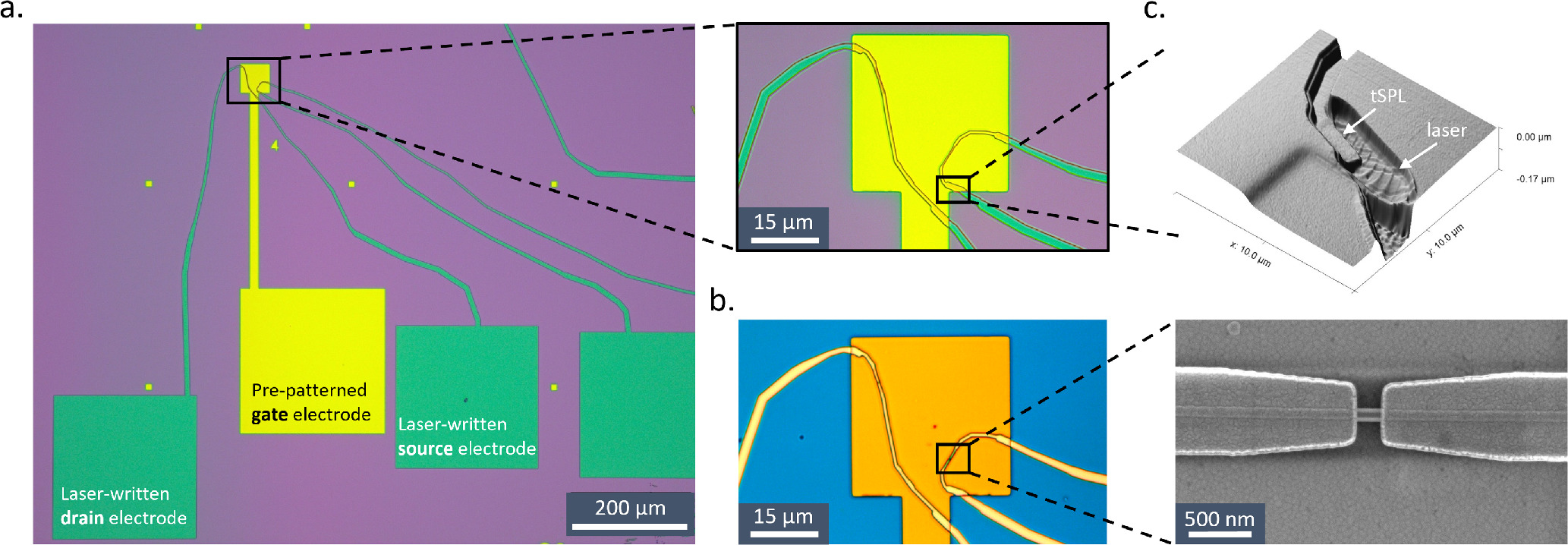
Figure 2. (a) Full image of the patterned device after wet etching, the large vias and the pads were patterned using the laser and the high-resolution electrodes were patterned using the t-SPL. (b) Optical image of the devices after metal deposition and lift-off, a zoom in SEM image of the spacing is shown on the right panel. (c) Topography scan of the overlap area between the t-SPL and the DLS written areas of the electrode lines, showing a continuous electrode line across both areas.
Download figure:
Standard image High-resolution imageThe right panel in figure 2(b) shows a SEM image of the measured device after wet etching the PMMA/MA using a mixture of 5 vol% DIW in IPA, ion milling and metal deposition. The Ti/Au electrodes are shown in yellow, the NW in blue and the Au-AlOx back gate in purple.
The ability to use the thermal scanning probe to image the NW through the resist stack without causing damage to either the resist or the wire enables precise patterning of devices with narrow contact spacing, as well as, in principle, the incorporation of side gates in close proximity to the wire for enhanced tunability (though here we used a single metallic back gate).
Figure 3 shows the electrical characterization of the NW device, a thin InSb nanowire with electrodes spacing of ∼200 nm. The electron mean-free-path of InSb nanowires is ∼100–300 nm [2, 31] and therefore, when applying Vbias across 200 nm long 1D channel the transport behavior is expected to be quasi-ballistic and the conductance as a function of gate voltage (Vg) should ideally increase in integer steps of 1G0 ( ) if effects from the contact-induced band-bending are minor [26, 32]. However, if there are substantial impurities, this can introduce scattering sites that can lead to the suppression of ballistic transport.

Figure 3. Electrical characterization of the patterned thin InSb device. (a) Differential conductance (dI/dV) versus Vsd and Vg of the device with contact spacing of ∼200 nm at zero magnetic field. (b) A series of line cuts from the 2D differential conductance map figure 3(a) Vsd = −3 mV and Vsd = 3 mV as a function of Vg with interval of ∼0.85 mV, blue and red curve respectively. (c) Differential conductance (dI/dV) versus Vsd and Vg under 2.8T out-of-plane magnetic field. (d) A series of line cuts from the 2D differential conductance map figure 3(c) map Vsd = −3 mV and Vsd = 3 mV as a function of Vg with interval of ∼0.85 mV, blue and red curve respectively.
Download figure:
Standard image High-resolution image
Figure 3(a) shows the conductance in the units of G0 as a function of source-drain voltage (Vsd) at a given Vg. The conductance increases as a function of Vg, a typical behavior for a semiconducting NW. In addition, the NW is not conducting at zero Vg which suggests that it is relatively free of accidental dopants. The differential conductance plot in figure 3(a) and the line cuts (figure 3(b)) that were extracted from figure 3(a) show oscillations that could be related to Fabry−Pérot (FP) interference, which occurs when electron waves traverse a partially transmitting cavity [26, 33]. This would imply phase coherence of the electrons over the device length. In addition, the conductance values evolve along plateau-like regions with values around a few G0, consistent with transport through a small number of quantum modes.
Applying out-of-plane magnetic field can lead to dephasing between multiple trajectories and thus suppress the FP oscillation and lead to the emergence of conductance plateaus. In addition, it is expected to lead to Zeeman splitting of subbands and hence plateaus near both integer and half-integer values of G0 [2]. Figure 3(c) shows the differential conductance plot in units of G0
 as a function of Vsd at a given gate voltage (Vg) under magnetic field of 2.8 T out-of-plane to the substrate. Linecuts of the conductance map (figure 3(d)) show that at these finite values of the magnetic field, the FP oscillations appear to be suppressed. In addition, it appears that between Vsd = −3 mV and Vsd = 3 mV the lines coalesce into plateau-like features at ∼0.5 G0 and ∼1.5 G0 as Vg is varied, possibly due to Zeeman splitting of the subbands, further suggesting that transport is quasi-ballistic over the inter-contact distance and is mediated by a small number of quantum modes in this range of Vg.
In conclusion, we demonstrated the ability to pattern nanowire devices using a mix and match writing approach, with a single hybrid lithography tool on the same resist stack, and with a single pattern transfer step. The thermal scanning probe was used for both the writing and reading of nanoscale electrode features, while the direct laser writer head was employed for the micron and millimeter sized leads and contact pads. The in situ thermal nanoimaging capability of the ultra-sharp tip was exploited for the precise markerless overlay of the contact on the nanowire. Moreover, the patterning was carried out in a closed-loop manner, eliminating the need for additional metrology tools to examine the quality and topography of the patterned structures separately. Within one hour of combined t-SPL and laser writing, we achieved a device with contact spacing of ∼200 nm that showed quasi-ballistic, phase-coherent transport. By integrating nanoscale and microscale lithography methods and bypassing the necessity for separate alignment markers, this approach holds promise for expediting the prototyping of quantum devices. Specifically, it could streamline the fabrication process of quantum devices, which traditionally require multiple gates to tune a one-dimensional wire, without the need to expose to the wire to SEM for high resolution alignment, see for example [34]. In addition, using t-SPL could potentially prevent damage induced by the electron beam, including the formation of charge traps in the nanowire and dielectric layers. Moreover, the ability to fit the tool in glove-box and use water-free developers, e.g. Ethanol instead of DIW:IPA, may allow further reduction of fabrication induced disorder by eliminating the need to break the native oxide shell using ion milling or sulfur passivation if the NWs are transfer dierectly from the growth system to the glovebox [35]. Taken together, along with other measures such as choice of nanowire materials, dielectrics and device layout, these factors could facilitate the development of low-defect quantum devices based on semiconductor nanowires.
Acknowledgments
This work was supported by the Department of Energy under Award No. DE-SC0019274. Portions of this work (nanofabrication) were conducted in the Minnesota Nano Center, which is supported by the National Science Foundation through the National Nanotechnology Coordinated Infrastructure (NNCI) under Award Number ECCS-2025124. Parts of this work (SEM characterization) were carried out in the Characterization Facility, University of Minnesota, which receives partial support from the NSF through the MRSEC (Award Number DMR-2011401) and the NNCI (Award Number ECCS-2025124) programs. Nanowire growth was supported by the European Research Council (ERC TOCINA 834290). TU/e acknowledges the research program 'Materials for the Quantum Age' (QuMat) for financial support. This program (registration number 024.005.006) is part of the Gravitation program financed by the Dutch Ministry of Education, Culture and Science (OCW). We gratefully acknowledge the Binnig and Rohrer Nanotechnology Center (BRNC) of IBM Research for providing access to their state-of-the-art clean room facility and resources, which were instrumental in conducting several experiments crucial to this study. We extend our appreciation to the operation staff and researchers at the lab for their invaluable support and assistance throughout this endeavor.
Data availability statement
All data that support the findings of this study are included within the article (and any supplementary files).
Supplementary data (0.6 MB PDF)