
Abstract
The fabrication and characterization of steep slope transistor devices based on low-dimensional materials requires precise electrostatic doping profiles with steep spatial gradients in order to maintain maximum control over the channel. In this proof-of-concept study we present a versatile graphene heterostructure platform with three buried individually addressable gate electrodes. The platform is based on a vertical stack of embedded titanium and graphene separated by an intermediate oxide to provide an almost planar surface. We demonstrate the functionality and advantages of the platform by exploring transfer and output characteristics at different temperatures of carbon nanotube field-effect transistors with different electrostatic doping configurations. Furthermore, we back up the concept with finite element simulations to investigate the surface potential. The presented heterostructure is an ideal platform for analysis of electrostatic doping of low-dimensional materials for novel low-power transistor devices.
Export citation and abstract BibTeX RIS

Original content from this work may be used under the terms of the Creative Commons Attribution 4.0 licence. Any further distribution of this work must maintain attribution to the author(s) and the title of the work, journal citation and DOI.
1. Introduction
Among the most important challenges in modern transistor development is the reduction of the power dissipation. Almost all integrated circuits in consumer electronics are made of silicon-based metal oxide semiconductor field-effect transistors (MOSFET). Over the last decades the increase of performance while decreasing the power dissipation has been achieved by scaling down the MOSFET's geometry. Eventually, this long-term scaling reached tremendous difficulties due to short channel effects, such as drain induced barrier lowering [1]. One approach to mitigate short channel effects are FinFET devices [2], which were successfully scaled down to the sub 22 nm regime. Recently, leading semiconductor companies like IBM introduced the 2 nm technology node, with a typical gate length of 14 nm and a 44 nm pitch. A key challenge thereby remains to maintain sufficient electrostatic gate control for ever smaller gate lengths and decreasing power. One approach is to design devices where the channel material and geometry are fundamentally different from state-of-the-art transistors [3–5]. Materials of lower dimensions, such as one-dimensional (1D) materials like nanowires (NWs) or carbon nanotubes (CNTs), and two-dimensional transition metal dichalcogenides (2D-TMDs) offer new design opportunities [5–7]. These materials allow to drive relatively high currents despite their almost atomically constrained geometry. Furthermore, these 1D or ultra-thin channel materials enable excellent gate control and extreme scalability. There are a number of TMDs that exhibit very small bandgaps well below 1 eV, which makes them ideal candidates for novel low-power transistor devices. Examples of such new devices include steep slope transistors (SSTs), such as tunneling field-effect transistors (TFETs) and superlattice energy-filtering transistors (EF-FETs) [8–16].
Manufacturing of SSTs with 1D- or 2D-materials in transistor applications demands an adjustable doping profile along the channel. However, conventional doping using implanted impurities or chemical modification will negatively impact the carrier mobility, generates unwanted depletion effects, and is also rather difficult or simply impossible to realize [17, 18].
An alternative to provide a semiconductor with a high electron or hole density is electrostatic doping via mutually insulated gate electrodes [19, 20]. This allows for individually controllable potentials along a semiconductor channel region, which enables the fabrication of reconfigurable transistors [21–23]. For example, a TFET channel needs at least three individually controllable gate electrodes in close proximity to precisely define the source-channel-drain band configurations in order to control the band-to-band tunneling probability [6, 24–26]. A previous approach that allows electrostatic doping with a so-called triple gate architecture was reported by Müller et al [12, 26]. The architecture included a lateral design of buried v-shaped metal center gate electrodes surrounded by n-doped silicon side gate electrodes. The platform is based on sophisticated fabrication methods such as ion doping for the side gates and chemical mechanical polishing (CMP) for the required planarization of the surface. Moreover, the v-shaped center gate electrodes are prepared by anisotropic wet-chemical etching, which hinders further downscaling of the lateral dimensions. Besides technical challenges during fabrication, a major drawback of the architecture is that the layout does not allow for a perfect overlap of the buried electrodes, which limits the steepness of the electrostatic doping profiles. Thus, fabrication of buried and individually controllable electrodes to achieve a field distribution with steep potential gradients along the channel remains an unresolved problem.
In this work, we report on the design and fabrication of a novel graphene/metal heterostructure with three mutually insulated and independently addressable gate electrodes. This heterostructure can be used as a platform for application and analysis of electrostatic doping of low-dimensional materials. The fabricated platform consists of structured graphene center gate electrodes buried by an oxide, on top of embedded titanium side gate electrodes and separated by an additional (intermediate) oxide. The use of 2D graphene as electrode provides a platform with high surface planarity. In contrast to the architecture reported by Müller et al [12, 26], our heterostructure is fabricated using much simpler methods. Furthermore, simulations highlight that much steeper electrical potential gradients between the gates can be achieved. The heterostructure allows symmetric n–n (nFET) and p–p (pFET) doping profiles, or asymmetric doping profiles for n–p or p–n band-to-band TFETs, respectively. For npn or pnp, two on-states are possible yielding a double tunneling barrier. We demonstrate the feasibility of our design utilizing CNTs as channel material with a channel length of 1.4 μm. Our design is versatile, and allows for the integration of almost any semiconducting 1D- or 2D-material and progressive scaling down to sub-100 nm dimensions.
2. Concept and layout
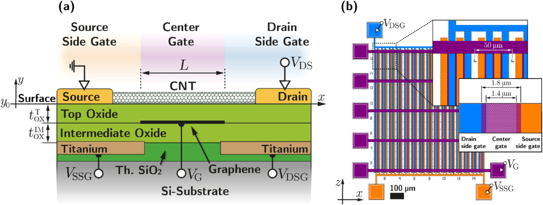
A simplified cross-sectional schematic of the platform is shown in figure 1(a). Titanium source side gates (SSG) and drain side gates (DSG) are embedded into an oxidized silicon substrate. The two side gates are buried beneath an intermediate oxide with a slightly laterally overlapping center gate electrode on top. The stack is then buried again by another (top) oxide. Figure 1(a) shows a CNT-FET device with the channel length L as an example. The orange-colored background marks the influence of the SSG zone, blue the DSG zone and purple the center gate zone, respectively. Figure 1(b) illustrates a bird's eye view of the design by showing the layout of the lithography mask. The same color scheme as in figure 1(a) is used to indicate the different layers representing the buried gate electrodes. The layout of the side gates can be best described as an interdigital comb-like architecture. All gates are arranged in an alternating and repeating pattern covering a large amount of the sample's surface, thus providing a high probability for nano-objects, i.e. 1D or 2D materials, to span over all three gates. Since all gates are individually addressable by external voltage probes, the doping level can be fully controlled during operation.

Figure 1. (a) Concept of the heterostructure depicted as a completed CNT-FET device. Titanium is used as side gate material embedded in thermal SiO2 (Th. SiO2) and complemented by a graphene center gate. (b) Lithography mask layout of a single heterostructure cell. The orange and blue layers are the side gates forming an interdigital comb-like architecture. The purple layer is the main gate or center gate.
Download figure:
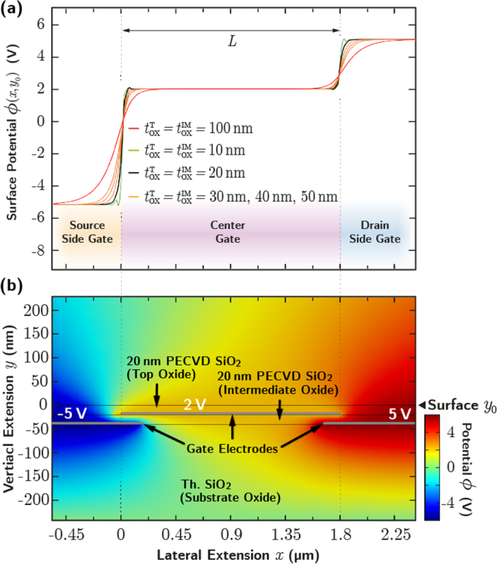
Standard image High-resolution imageThe platform is designed to provide arbitrary electrostatic doping profiles for various steep slope devices including TFETs. This requires a very sharp potential barrier to realize steep transitions from the source/drain conduction band to the channel valence band in order to achieve a high band-to-band tunneling probability [8, 27]. That is, the steeper the potential transition, the higher the gate control for the device. The electrostatic potential distribution along the heterostructure has been investigated by finite element (FE) simulations using Comsol Multiphysics. The Fermi-level of the low dimensional material on top of the heterostructure can be shifted by electrostatic doping, which effectively results in tunable doping profiles. Thus, the gradient of the surface potential induced by the three buried electrodes is directly related to the local doping profile of the low dimensional channel material. Figure 2(a) shows the surface potential distribution along all three gates with different oxide thicknesses tox, respectively. We plotted the potential profiles in y-direction at the surface for tox = 10 nm, 20 nm, 30 nm, 50 nm and 100 nm (identical increment for intermediate and top oxide). Figure 2(b) illustrates the surface potential as a 2D plot with the corresponding electrodes. Voltages are arbitrarily chosen here and depend on the actual channel material. As expected, the sharpness of the potential decreases for greater vertical distances of the electrodes, thus weakening the band transitions. Therefore, the electrostatic doping gradients depend significantly on the oxides' thickness and should be as thin as possible.

Figure 2. (a) FE simulations of the potential with different oxide thicknesses at the surface y0. Here we chose an equal increment for the intermediate and the top oxide, respectively. Note that voltages are chosen arbitrarily since they only scale the curves but do not affect the potential characteristic. (b) 2D FE simulation cross-section plot of the potential distribution of the heterostructure. The buried gate electrodes are drawn as gray bars.
Download figure:
Standard image High-resolution imageThe advantage of using graphene for the center gate electrode instead of using a conventional metal-based electrode is the ultra-thin thickness of the graphene layer. Replacing the graphene layer by a conventional metal layer (with a thickness of some tens to nanometers) would significantly increase the distance between the side gates and channel material. This would result in less sharp potential gradients. We expect that unintentional doping of the graphene from the side gate potentials is of no concern here. A noticeably decline of the density of states of the graphene center gate would appear by moving the Fermi-level to the very vicinity of the Dirac-point. A static potential configuration from the side gates coinciding with such event is highly unlikely and would be detectable in the transfer characteristics. A change of the graphene conductivity by unintentional electrostatic doping would also not affect the platform's functionality since the graphene is used as biasing electrode only and does not drive any significant current apart from leakage currents in the ∼pA range, see below. Furthermore, the contact to the intermediate oxide will result in chemically doping of the graphene, which provides available states for charge carriers at the interface.
Since we already mentioned the previously reported triple gate architecture by Müller et al [26], we also compared the potential transition between the two designs (figure 3). Due to the lateral structure used by Müller et al the electrode line-up is discontinuous. The simulations showed that a lateral formation of electrodes does not provide as much steepness as our approach of overlapping electrodes with an intermediate oxide. According to the simulation shown in figure 3, the width (10% to 90%) of the transition between the SSG and center gate, and center gate and DSG are 6 nm (1) and 13 nm (2) for our new platform (for 10 nm and 20 nm oxide thickness, respectively), and 37 nm (3) for the architecture reported by Müller et al. Thus, our concept allows for inherently steeper electrostatic doping profiles. The band-to-band tunneling probability depends exponentially on the length of this transition region, and thus the steepness of the potential gradients. Another disadvantage of Müller's platform is that it relied on n-doped silicon side gates (in this case the side gates could not be replaced by metal layers since the silicon is required for anisotropic etching). As a semiconducting electrode the side gate edges exhibit a depletion zone for positive voltages adding to the issue of discontinuous potential transitions.

Figure 3. Potential distribution corresponding to the electrostatic doping profile of a channel material for different buried triple gate architectures: Steepest transition is shown by curve (1) and (2) representing our design with tox = 10 nm and tox = 20 nm, respectively (for both intermediate and top oxide thickness). The design by Müller et al [26] exhibits a noticeably weaker slope (3) in the potential transition (curves had been adjusted to match the channel dimensions of each platform). The curve (3) is reproduced with permission from [28]. © Verlagshaus Mainz (2015). Note, additional depletion effects of the Si side gates are not considered for slope (3).
Download figure:
Standard image High-resolution image3. Experimental
3.1. Heterostructure platform fabrication
Fabrication of the heterostructure starts with the wet-thermal oxidation of a 4 inch silicon wafer. The targeted SiO2-thickness depends on the desire to improve optical visibility of the buried graphene layer. According to our previous simulations maximum visibility is achieved for a SiO2 thickness of 72 nm [29]. For integration of the side gates into the heterostructure while still maintaining a nearly planar surface, a reactive ion etching (RIE) process etches 30 nm trenches into the SiO2 which are filled with titanium in a subsequent sputtering deposition process. A CMP process for planarization is not required when the trench etching and metal sputtering process are precisely calibrated (see figure S1a in the supplementary data). Titanium is chosen because it exhibits a very low thermal expansion coefficient (8.5 10–6 K−1), which is similar to the thermal expansion coefficient of SiO2 (5.1 10–6 K−1), and thus allows for a planar surface by preventing any damage of the substrate at elevated temperatures. This is important since the subsequent plasma enhanced chemical vapor deposition (PECVD) is carried out at 350 °C for 30 s using an Oxford PlasmaLab 80Plus system in order to deposit 20 nm of SiO2 onto the substrate. As a precursor gas we used 2% SiH4 in He (flow rate 192 sccm, N2O flow rate 355 sccm) a plasma power of 50 W and a pressure of 1.33 hPa. The Ti metallization limits our platform's temperature, which is in the range between cryogenic temperatures and at least up to 350 °C. Up to this point, all processes were carried out at wafer-level, which allows for high throughput fabrication. The main or center gates on top of the oxide are made of transferred graphene. We employ such transfer of graphene based on simplicity. Note that various direct growth approaches for graphene have been reported that potentially could allow transfer-free pathways [30]. However, our platform does not have stringent demands for a high electronic quality of the graphene layers. We used copper foil catalyzed chemical vapor deposition (CVD) of graphene and a subsequent simple PMMA-based wet-transfer as proposed by Deokar et al [31]. For this step, the wafers were diced into 1.2 cm × 1.2 cm sized samples to allow transfer of 1 cm × 1 cm sized graphene sheets. The transfer process causes a relatively high surface roughness of 8 nm (see figure S1(b) in the supplementary data). This roughness may lead to a non-perfect alignment of the CNT to the surface, and thus a limited transistor performance. By using an optimized transfer process, a much lower surface roughness could be achieved. For example, Zhang et al reported on a Rosin-enabled transfer yielding a graphene surface roughness of 0.66 nm [32]. However, for this proof-of-concept we do not focus on optimization or development of a new transfer process, and alternative methods such as wafer-scale transfer [33] or bubble transfer of graphene e.g. CVD-grown on germanium wafers [34] can also be used. Different from the process reported by Deokar et al, we found that a bake-out for five minutes on a hotplate at 70 °C removes the residual water on the substrate more efficiently. PMMA residues are then removed by acetone at 40 °C. Note that resist residuals are a general issue for PMMA based transfer methods [35]. In fact, resist residuals may significantly increase the contact resistance at the metal interface [36]. A cleaning with oxygen plasma would almost fully remove the PMMA, however, the graphene would be removed as well. Therefore, the substrate stays at least three hours in hot acetone (40 °C) to remove as much residues as possible. Thereafter, UV-lithography and a 30 s Ar/O2-RIE process patterned the graphene into the slightly overlapping center gate structure. The 20 nm top oxide is subsequently deposited by the same PECVD process as carried out for the intermediate oxide. Exemplary images of the completed platforms are shown in figure 4. The overall gate length is 1.8 μm for 1.4 μm side gate separation, which is the smallest feature size on the platform allowing a processing sequence solely based on optical lithography. The entire process could alternatively be fabricated by any other high-resolution lithography method including electron beam lithography. This would allow to scale down to gate lengths below the 100 nm regime.

Figure 4. Optical (left) and scanning electron microscope (SEM, right) images of the completed platform with metal contact terminals before transistor fabrication: the upper and lower terminals connect to each pair of the titanium side-gates (silver-ish), terminals left and right connect to the graphene center gates (blue-colored electrodes). The graphene is barely visibly in the SEM microscope.
Download figure:
Standard image High-resolution image3.2. Transistor fabrication
As an experimental proof-of-concept we demonstrate the working principle of our new platform for arbitrary electrostatic doping profiles by using field effect transistors based on carbon nanotubes. Commercially available single wall CNTs were purchased from IoLiTec Ionic Liquids Technologies GmbH (Lot NCPCS009) and solved in isopropyl alcohol. The CNTs were then deposited onto the sample's surface by spin-on. Due to the high density of the triple gate areas, the chances are relatively high to find a suitable CNT laying across all three gates. This method however causes a randomized positioning of CNTs, which makes further contact fabrication with UV-lithography impossible. Therefore, source and drain contact terminals were patterned by electron beam lithography (EBL) using the CSAR62 resist (AR-P6200 by AllResist GmbH) and a Raith Pioneer System with 15 kV accelerating voltage. For the removal of the resist after metal deposition (lift-off) the exposure must cause the resist to exhibit a small undercut after developing. This is achieved by an exposure dose of 90 μC cm−2 eventually yielding very good lift-off results in dioxolane and acetone. Metal deposition (60 nm Au) was carried out by thermal evaporation to provide high deposition anisotropy. Figure 5 shows a completed CNT-FET device with deposited metal source and drain contacts. As an alternative to CNTs, which are randomly distributed after spin-on, 2D-TMDs such as 2D-WS2 could be deposited using a transfer [37] or even low temperature growth process for example. In this case, alignment and layout of the transistor structures could be precisely prepared by conventional patterning processes including simple UV-lithography.

Figure 5. Completed CNT-FET on the substrate's surface: the example shows the metal S/D-contact terminals connected to the CNT laying across the center gate and both side gates on top of the heterostructure.
Download figure:
Standard image High-resolution image3.3. Metrology
Raman spectroscopy of graphene was performed with a Renishaw Raman InVia microscope using a 50× objective lens and a 532 nm laser excitation at 1% power (10 s exposure time, 3 accumulations). Scanning electron microscopy (SEM) images were obtained using a Zeiss Gemini Column within a Raith Pioneer System. For electrical characterization, a triaxial probe needle station with variable chuck temperature was used. The current/voltage characteristics were measured using an Agilent 4156C semiconductor analyzer (20 ms integration time).
4. Results and discussion
To evaluate the impact of plasma enhanced oxide deposition on the graphene layer, Raman measurements have been conducted. Figure 6 shows the Raman spectra before and after oxide deposition, respectively. The marked peaks reveal information about the graphene's morphology [38]. The D-peak reflects the likelihood of any scattering events happened with a lattice defect. Therefore, the smaller the D-peak, the smaller the defect concentration of the graphene [39]. Note that even for plain graphene without oxide deposition a D-peak appears, suggesting that the transferred graphene already exhibits some defects. However, an increase of defects after a wet-transfer of graphene is quite common and can be alleviated by time consuming procedures [35, 40]. The defect concentration is usually related to the quality of graphene, and the ratio of D- to G-peak makes a good indicator for evaluating the graphene's quality. Here, the D/G-ratio is 0.14 for the graphene before and 0.5 after the oxide deposition. According to Cançado et al this translates to approximated defect distances of LD > 24 nm and >15 nm, respectively [41]. However, the Raman spectra suggest that even after oxide deposition, the graphene is still intact since the 2D-peak has only shifted by ∼10 cm−1 from the graphene's characteristic signature 2D-peak at ∼2674 cm−1 [39]. We also confirmed the presence of intact graphene by crossway electrical measurements throughout the structured graphene before and after the oxide deposition. We found that the electrical resistance increased by only 17% on average after oxide deposition. For our heterostructures, the electrical properties of the graphene layers are of minor importance, since the graphene is only used for electrostatic biasing and does not drive any significant electrical current. Thus, we conclude that the buried graphene layer is suitable enough to serve as gate electrode.

Figure 6. Characterization of the graphene center gate layer: Raman spectra of the transferred graphene sheet before (black curve) and after (orange curve) the oxide deposition. Note that both spectra are not equally scaled in intensity.
Download figure:
Standard image High-resolution imageTo verify the functionality of the fabricated device, output and transfer characteristics were measured at different temperatures. Figure 7(a) demonstrates the field effect transistor behavior based on the transfer characteristics (drain current ID versus center gate voltage VG) at room temperature (295 K), at 373 K and at 423 K, respectively, on a semi-logarithmic scale. Source side gate and drain side gate are set to 3 V and −3 V, respectively, implementing an asymmetric pnn and ppn doping profile. As expected, the CNTs exhibits minimal p-type behavior due to the chemical doping effect of oxygen molecules adsorbed on their surface [42–44]. Since the side gates and the center gate are mutually aligned within the scope of optical lithography, a perfect overlap of the electrodes as suggested by FE simulations is not guaranteed for every sample. This and the non-optimized roughness of the graphene layer of 8 nm (see figure S1b in the supplementary data) results in an inverse subthreshold slope of 94 mV dec−1 and a threshold voltage of Vth ≈ −1 V (see figure S3 in the supplementary data) at room temperature (295 K). A much better lateral alignment accuracy could be achieved by optimization of the UV mask layout or using EBL for platform fabrication. In this case we expect much smaller inverse subthreshold slopes.

Figure 7. CNT-FET current/voltage measurements: (a) transfer characteristic at different temperatures on a semi-log scale, drain-source voltage was set to VDS = 150 mV. Source side gate and drain side gate are setup in a static asymmetric configuration: VSSG = 3 V, VDSG = −3 V. (b) Corresponding gate leakage current IG (center gate) versus VG with a maximum absolute current of IG = 1.5·10–11 A. (c), (d) Output characteristic at different temperatures for different gate voltages ranging from −3 to −1.5 V with the same side gate configuration. (e) Transfer characteristic for a symmetric doping profile (red curve: VSSG = VDSG = 3 V, blue curve: VSSG = VDSG = −3 V). (f) Transfer characteristic for floating side gates (blue curve) and for a gate union VSSG = VDSG = VG.
Download figure:
Standard image High-resolution image
The drain current ID exhibits an on/off ratio of ∼5 decades, which comes close to the recommendation of 6 decades by the International Roadmap for Devices and Systems (IRDS) [45]. With rising temperature, the on/off ratio reduces to ∼4.2 decades at 373 K and ∼3.3 decades at 473 K, respectively. This agrees to previous studies, which found that CNT-FET devices exhibit a lower dependence on temperature than MOSEFTs [46–48]. The overall center gate leakage current as illustrated in figure 7(b) is larger than for top gate architectures [49–51]. That is because the electrodes of source and drain cover a relatively large area on the surface all across the buried gate architecture, which eventually increases the possibility for leakage currents adding to the drain current at VG = 0 V. This also contributes to the large inverse subthreshold slope and can be mitigated by improving the resistivity of the deposited oxides. However, the gate current here is still low enough for a proof-of-concept and has only a small impact on the drain current characteristic.
Figures 7(c) and (d) show the output characteristics for different gate voltages ranging from −3 to −1.5 V at different temperatures. We estimated the hole mobility μh (p-type, ppn) at room temperature from the transconductance dID/dVG = μh(C/L2)VDS at VDS = 25 mV. Where L = 1.8 μm is the CNT length, and C the capacity per unit length approximated by a cylindrical geometry, i.e. C/L = 2πε0 εox/ln(2dox/r). ε0 is the permittivity of vacuum and r the CNT radius. According to the supplier of the CNTs, the radius is in-between r = 1 nm and r = 2 nm. Since the energetic alignment of the intrinsic region is controlled by the center gate we use dox = 20 nm, that is the thickness of the top oxide, and a relative permittivity for SiO2 of εox = 3.9. From figures 7(c) and (d) we find dID/dVG = 5 nA V−1 in the saturation regime. Thus, the calculated hole mobility is between μh = 49.6 cm2 V−1 s−1 (for r = 2 nm) and μh = 61.1 cm2 V−1 s−1 (for r = 1 nm), which is comparable to that of previous CNT-FET studies [52–54]. Additionally, we altered the doping configuration to a symmetric setup to investigate the impact of the side gates. Figure 7(e) shows how the performance is drastically reduced for npn to nnn and pnp to ppp configurations. In case of disabling (floating contacts) the side gates all along (figure 7(f)—blue curve) or in case of short-circuiting all side gates (figure 7(f)—red curve) the performance is better than for symmetric doping, but still inferior to asymmetric doping. The minimum ID off-current at VG = 0 V is about an order of magnitude lower since the side gate potential does no longer contribute to the overall channel potential. A similar performance is observed for a single-gated CNT as shown in figure S2 in the supplementary data. In this configuration the subthreshold behavior is dominated by the thermally broadened Fermi distribution, which results in a much larger inverse subthreshold slope of S−1 = 198 mV dec−1 compared to 94 mV dec−1 for triple-gated asymmetric doping. Obviously, the asymmetric doping has a strong impact on the transistor performance. In this context it is important to note, that the inverse subthreshold slope with asymmetric doping is also not affected by the temperature (see figure 7(a)). Therefore, we conclude that the charge transport for a CNT with asymmetric doping is indeed dominated by band-to-band tunneling. Further optimization of the platform (such as better alignment of the CNT to the surface, thinner top and intermediate oxide, and replacement of SiO2 by an oxide with larger εox like Al2O3) may allow to further decrease the inverse subthreshold slope potentially even below the thermoionic limit of 60 mV dec−1 at room temperature.
To put our research into perspective, table 1 lists a comparison of similar devices with respect to the inverse subthreshold slope S−1, the maximum drain on- and minimum off-current ID,On and ID,Off, respectively, the channel and contact-material, and the platform used for gating. Note, the table makes no claim to completeness and in general comparison between difference devices is difficult due to different device geometries, CNT/NW radius, oxide thickness, etc. Relatively small S−1 are reported for top-gated CNTs in this table [55, 56]. However, for these devices, the ratio ID,On:ID,Off is only 2–3 orders of magnitude, which is considered to be too low for most applications. A much larger ID,On:ID,Off of 9 orders of magnitude has been reported for a double top-gated silicon nanowire (Si-NW) with an inverse subthreshold slope of 90 mV dec−1 [57], which is comparable to our asymmetrically doped CNT. In this device, one gate electrode is used to control the field effect while the other gate electrode can be used to electrostatically program the device into n-type or p-type operation. However, similar to single-gated configuration and in contrast to the here proposed heterostructure, the minimum inverse subthreshold slope that can be achieved is fundamentally limited to the thermally broadened Fermi distribution.
Table 1. Comparison of recent studies on similar devices, with sgFET = single gated field effect transistor, TFET = tunnel field effect transistor, BTG = buried tripe gate and BSG = buried single gate. The characteristics of the single-gated CNT with BSG platform is shown in figure S2 in the supplementary data.
| Channel material | S−1 (mV dec−1) | ID,On (A) | ID,Off (A) | Contact material | Platform | References |
|---|---|---|---|---|---|---|
| CNT | 94 | ∼3.5 × 10⁻⁸ | ∼5 × 10–13 | Au | TFET, BTG | This study |
| WSe2 | 180 | ∼1·10−6 | ∼9 × 10⁻¹² | Ni | TFET, BTG | [58] |
| CNT | 198 | ∼10−8 | ∼2 × 10⁻¹⁴ | Au | sgFET, BSG | This study |
| CNT | 85 | ∼2 × 10⁻⁶ | ∼3 × 10⁻⁹ | Co–Mo alloy | sgFET, Top-Gate | [55] |
| CNT | 73 | ∼8 × 10⁻⁶ | ∼5 × 10⁻¹⁰ | Ti/Au to graphene | sgFET, Top-Gate | [56] |
| Si-NW | 90 | ∼2 × 10⁻⁶ | ∼4 × 10⁻¹⁵ | NiSi2 | Double Top-Gate | [57] |
The CNT-FET measurements demonstrated the working principle of our new heterostructure for electrostatic doping of low-dimensional materials. The platform is universal and can be used for application and analysis of electrostatic doping of various 1D- and 2D-materials. As a proof-of-concept, the heterostructures were fabricated using UV-lithography, demonstrating that steep electrostatic potential gradients can be achieved using even very simple patterning technologies. In contrast to the concept reported by Müller et al [12, 26], further improvement and lateral downscaling well below the 100 nm lateral dimensions can be obtained using mask optimization or high-resolution pattering technologies, including electron-beam lithography. In addition, the steepness of the doping gradient strongly depends on the oxide thicknesses (see figure 3). For simplification of the fabrication process, we used relatively thick (20 nm) SiO2 layers prepared by a well-established PECVD process, to ensure low leakage currents from the buried gate electrodes to the source- and drain-contact pads. Further optimization of the SiO2 PECVD process may allow for much thinner oxide layers. Instead of PECVD, ozone-enhanced thermal atomic layer deposition of ultra-thin and highly insulating oxides (well below 10 nm) on graphene could also be used providing even sharper potential gradients [52, 59]. Moreover, in follow-up studies, the simple graphene transfer process could be replaced by a high-quality wafer-scale transfer or (potentially) even direct growth of graphene on oxides for complete wafer-scale fabrication of the heterostructures. We also note that recently established techniques using computer vision to find isolated CNTs, followed by automated electrode routing, could be used to increase the manufacturing throughput of these randomly distributed CNT devices [60].
5. Conclusions
In this study we demonstrated the feasibility of a graphene heterostructure to implement an individually configurable electrostatic doping profile for a CNT-FET device. Fabrication of the platform was done by conventional UV-lithography partially on wafer-scale to establish a simple and reproducible process while still being able to convey fabrication to high resolution pattering technologies. Proof-of-concept electrical measurements of CNT-FET devices demonstrated field-effect transistor characteristics with an inverse subthreshold slope down to 94 mV dec−1. Smaller inverse subthreshold slopes may be achievable by optimizing the patterning process, the intermediate oxide thicknesses and buried electrode overlapping. Increasing the temperature showed a decrease in performance, however, less pronounced than for conventional MOSFET devices. A variation in the doping profile was successfully shown for a number of possible configurations, such as asymmetric doping (pnn, ppn) and symmetric doping (npn, nnn and pnp, ppp). The demonstrated platform can be used for application and analysis of electrostatic doping of emerging low-dimensional materials including 2D dichalcogenides such as WS2 or WSe2 and may unlock their application potential for novel steep slope transistor devices.
Acknowledgments
JAA-W acknowledges the support of his Royal Society Dorothy Hodgkin Research Fellowship. SH acknowledges funding from EPSRC (EP/P005152/1).
Data availability statement
The data that support the findings of this study are openly available at the following URL/DOI: http://hdl.handle.net/2003/41227.
Supplementary data (0.4 MB PDF)