

Abstract
With the advent of graphene, there has been an interest in utilizing this material and its derivative, graphene oxide (GO) for novel applications in nanodevices such as bio and gas sensors, solid-state supercapacitors and solar cells. Although GO exhibits lower conductivity and structural stability, it possesses an energy band gap that enables fluorescence emission in the visible/near infrared leading to a plethora of optoelectronic applications. In order to allow fine-tuning of its optical properties in the device geometry, new physical techniques are required that, unlike existing chemical approaches, yield substantial alteration of GO structure. Such a desired new technique is one that is electronically controlled and leads to reversible changes in GO optoelectronic properties. In this work, we for the first time investigate the methods to controllably alter the optical response of GO with the electric field and provide theoretical modeling of the electric field-induced changes. Field-dependent GO emission is studied in bulk GO/polyvinylpyrrolidone films with up to 6% reversible decrease under 1.6 V µm−1 electric fields. On an individual flake level, a more substantial over 50% quenching is achieved for select GO flakes in a polymeric matrix between interdigitated microelectrodes subject to two orders of magnitude higher fields. This effect is modeled on a single exciton level by utilizing Wentzel, Kremer, and Brillouin approximation for electron escape from the exciton potential well. In an aqueous suspension at low fields, GO flakes exhibit electrophoretic migration, indicating a degree of charge separation and a possibility of manipulating GO materials on a single-flake level to assemble electric field-controlled microelectronics. As a result of this work, we suggest the potential of varying the optical and electronic properties of GO via the electric field for the advancement and control over its optoelectronic device applications.
Export citation and abstract BibTeX RIS
1. Introduction
Soon after its discovery [1], graphene has acquired substantial interest in microelectronics industry due to its unique properties such as single-layer transparency [2, 3], high conductivity [4], and high mechanical strength [5–7]. However, due to the complexity and high cost of production, its less costly functional derivatives have become more widely used. Currently, graphene derivatives such as graphene oxide (GO) are already pioneering in the number of applications over its parent material [7]. Due to its large number of functional group-related defects, GO falls behind graphene in mechanical strength and conductivity [8]; however, it still remains a potential candidate for carbon microelectronics. These oxygen addends render GO soluble in water as well as in a variety of polar solvents [9, 10], which is critical for solution-based deposition. The ease in fabrication also adds an important advantage over graphene materials: GO can be prepared from graphite via a variety of chemical procedures including Hummers and modified Hummers methods [11, 12], oxidative techniques using benzyl peroxide [13], and other synthetic routes [14–16]. Finally, the presence of GO surface defects leads to a sizeable ∼1.5–2 eV band gap [14, 17, 18], enabling fluorescence in the visible tailing into the near-IR that can be utilized for optoelectronic and biomedical imaging applications [19–21]. Due to its versatility and optical properties, GO has been currently utilized in a number of devices including organic light-emitting diodes [22], solar cells [23], chemical sensors [24], flexible transparent electronics [25], and energy storage components [26].
The mechanism of GO emission is proposed to be excitonic in nature [27, 28], described by excitonic confinement [29] within the islands of sp2 graphitic carbon surrounded by the sp3-hybridized regions rich in functional groups [14, 30, 31]. The degree of oxidation can lead to changing the size of the graphitic regions, surrounded by sp3-hybridized barriers [26, 27, 32, 33], physically leading to the change in emission wavelength and alteration of GO fluorescence intensity [31]. Thus, chemically and/or physically manipulating GO structure including types/arrangements of functional groups may allow us to tune its behavior for a particular application [34]. Methods of chemical modification of GO platform developed to yield altered optoelectronic properties include controlled ozone treatment leading to the addition/alteration of oxygen functional groups [31], removal of polyaromatic highly oxidized fragments from GO surface reducing excimer formation [35], treatment with sodium dodecyl sulfate disrupting π–π stacking in GO and altering its electronic environment [36], hydrazine reduction leading to the conversion into a non-emissive rGO [37], surface amination and ring opening amination of epoxides in GO [38], and thermal treatment leading to the reduction and substantial decrease of emission intensity [14]. The aforementioned methods are reliable; however, they are laborious, hard to apply to solid-state devices, and mostly yield irreversible changes of GO properties.
In order to reversibly fine-tune GO optoelectronic behavior without significant alteration of its chemical structure, physical methods need to be developed. Thermal processing reducing the oxygen addends in GO could serve that purpose [14, 39], however; it can be detrimental to the device and hard to controllably introduce. More versatile electronic methods including current and/or electric field can be more effectively introduced within the circuit. The behavior of GO under electric current has been studied showing the deoxygenation of GO when a current is passed through it, leading to an increase in conductivity caused by the thermal reduction of GO from the Joule effect [32, 33]. Yao et al also reported GO film being partly reduced to rGO under an electric current with exponentially decreased resistance [40]. Although effective, this method of control substantially deteriorates the optical properties of GO and irreversibly changes the band gap which may not be desired in optoelectronics. Electric field-based methods for controlling optoelectronic properties of GO have not been developed to date. Applying an electric field is known to reversibly alter the excitonic emission of single-walled carbon nanotubes [41–43] by decreasing exciton recombination rates and promoting charge-induced fluorescence quenching. Considering the proposed excitonic nature of GO emission [14, 27, 30], we also expect the electric field to affect exciton recombination in GO and yield somewhat reversible changes in its fluorescence emission. In order to assess this effect in bulk and on the level of individual GO flakes, we subject GO films to the electric fields on the order of 1.6 V µm−1 in a parallel plate capacitor geometry inside the fluorescence spectrometer and GO flakes to two orders of magnitude higher fields between interdigitated electrodes (IDE) under the fluorescence microscope. The origin of GO emission quenching can be assessed based on the mechanism of the exciton recombination on the surface of GO flakes under the external electric field. The Wentzel, Kremer, and Brillouin (WKB) approximation provides calculated energy eigenvalues and the rate of tunneling of electrons out of the potential well [44], thus assessing the probability of recombination of the excitons in GO. Altering GO optoelectronic properties with the electric field may allow us to improve/tune the performance of GO optoelectronics, justifying the need for exploration in this work. Finally, it is worth exploring the potential of GO for electrophoretic manipulation on the individual flake level similar to that of single-walled carbon nanotubes [45].
2. Experimental section
2.1. Sample preparation
GO/polyvinylpyrrolidone (PVP) film was used to investigate the behavior of bulk GO under the electric fields. The film was made by mixing PVP powder (0.2 g) with 1 ml of aqueous dispersion of single-layer Hummers GO (p9, Goographene) at GO concentration of 5 mg ml−1. 1 ml of the gel dispersion was dropped and pressed uniformly between two transparent indium tin oxide (ITO) electrodes (2.5 cm2 × 2.5 cm2) in a parallel-plate capacitor geometry and oven-dried at 80°C to remove water. The thickness of the film was measured with a caliper. This type of design enabled in situ monitoring of GO fluorescence as the ITO/GO-PVP/ITO parallel plate capacitor was mounted in the sample chamber of a NanoLog Spectrofluorometer (J81096, Horiba Scientific). GO samples for monitoring individual flakes in the electric field under the microscope were pre-treated: single-layer GO aqueous dispersion at a concentration of 1 mg ml−1 was subjected to ultrasonic tip treatment (Q55, Qsonica) at 16.5 W for 5 min to reduce large size GO flakes. This suspension was later spin-coated with increasing rotational velocity for 5 min at varying volumes of 1–5 µl onto a 10 µm concentric gold IDE (G-IDECONAU10, Metrohm DropSens) with the goal of having the GO flakes in between the electrodes for microscopy experiments.
All these samples were subjected to an electric field using a power supply (2K-10, Power Designs Pacific, INC).
2.2. Fluorescence spectroscopy
To test the response of the fluorescence properties of GO to electric fields, bulk GO/PVP film layered in between transparent ITO electrodes was placed inside the NanoLog Spectrofluorometer's chamber at 45°. With an excitation of 440 ± 5 nm, the film was subject to electric fields ranging from 0 to 1.6 V µm−1 in increments of 0.2 V µm−1, and its emission in the visible/near-infrared (NIR) was collected by a Syncerity CCD Deep Cooled Camera (Syncer-1024 x 256-OE, Horiba Scientific) with an integration time of 6 s. The excitation power density is measured to be less than 1 mW cm−2, and the sample temperature measured by a thermocouple did not change during the experiment. A PVP background fluorescence (figure S1 (available online at https://stacks.iop.org/NANO/31/465203/mmedia), supporting Information) was subtracted from all the emission spectra. No breakdown current above 1 µA was detected throughout the experiments.
2.3. Microscopy
Fluorescence microscopy setup was based on semi-motorized inverted microscope (IX73P2F, Olympus) with visible/near-IR spectrally-resolved capability. GO emission was collected by an IR-corrected UPLANAPO 60 x /0.90 na objective (1-UB831, Olympus), imaged with CMOS (Prime 95B, Photometrics) camera, while all image-processing was done by the Micro-Manager 1.4 software. The images were timed to be taken at segmented time intervals corresponding to the incrementing electric fields with 200 ms exposure time. To test the properties of individual GO flakes, the IDE with dried GO flakes on their surface were placed in between the microscope slide and cover slip. Using a 460 ± 25 nm excitation filter and 655 ± 25 nm emission filter, GO flakes were imaged in the fluorescence microscope. The excitation power density was measured as 4 mW cm−2. The temperature of the observed sample did not change during the entire experiment. Single flake images were taken with an applied electric field that ranged from 0 to 160 in 10 V µm−1 increments until over 1 µA breakdown current was detected. Electrophoretic experiments were conducted with 1 mg ml−1 GO suspension in DI H2O that was drop-cast onto the IDE. Images of the flakes were then taken at the electric fields from 0 to 6 V µm−1 at increments of 1 V µm−1 until a substantial 1 mA current was detected.
2.4. Image analysis
The images of individual GO flakes were later post-processed through ImageJ software. The image processing included the background-corrected total flake fluorescence intensity and the statistical analysis. The mean background fluorescence was multiplied by the area of GO flake and was subtracted to the integrated density of the GO flake. The integral density is equivalent to the product of the area and the mean gray value, calculated using ImageJ tools. The baseline sample intensity collected without applied external field was subtracted from that of the electric field subjected to GO flake. The background for the correction was acquired by selecting regions nearby the flake that had no observable fluorescence. The spectra of GO emission in bulk GO/PVP film were smoothened by Origin 6.0 software for analysis.
2.5. Theoretical analysis
To describe the changes in the optoelectronic properties of GO, the WKB approximation was used to model tunneling of the electron from the exciton potential energy well. The ab initio potential energy well model associated with the GO system was created and assessed with and without the external electric field. The WKB calculations were performed using Wolfram Mathematica 11, assessing the rate of tunneling and relating it to the electron to the emission quenching probability. Further ab initio calculations were performed to assess the effective field within GO graphitic clusters.
3. Results and discussions
The control mechanisms such as electric current or electric fields available in microelectronic devices could be ideal for altering device performance. Given the drastic and irreversible reduction of GO with electric currents, a less destructive alteration of GO optoelectronic properties via the electric fields with no measurable current passing through the material is proposed. Those effects of the electric field on the GO optical properties are assessed via its fluorescence emission considered to occur across its band gap in the visible/NIR (figure 1(a)). Broad GO fluorescence spectrum can be attributed to collection of the overlapping features corresponding to the emission from different sizes of the islands of graphitic carbon [14]. Effects of the electric fields in bulk GO films are monitored in situ as GO incorporated in the PVP matrix is placed in a parallel capacitor geometry between the ITO-coated transparent electrodes and subjected to the electric fields inside the spectrofluorometer. Although PVP exhibits a weak fluorescence at 505 nm (figure S1), it does not interfere with the analysis of GO emission that peaks in the NIR at ∼700 nm (figure 1(a)). Additionally, the control PVP film does not show observable changes in its emission intensity under the electric fields of up to 1.6 V µm−1, which ensures that all the field-induced GO fluorescence changes are due to the alteration of GO optical properties only.
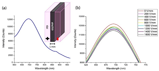
Figure 1. Fluorescence spectra of the GO/PVP film. (a) Emission of GO in GO/PVP film. Inset represents the schematics of the ITO electrode-encapsulated film. (b) Decrease in fluorescence intensity of GO as the film is subjected to the increasing electric fields.
Download figure:
Standard image High-resolution imageAs the GO/PVP film is subject to the fields of 0–1.6 V µm−1 incremented in 0.2 V µm−1 steps, the fluorescence intensity gradually decreases by up to 6% at the maximum field strength (figure 1(b)). However, after returning to 0 V µm−1, the fluorescence intensity increases back even above the initial value, suggesting a reversible electronic process (figure S2, supporting Information), where the functional groups are not reduced. An increased intensity of the restored fluorescence can be potentially attributed to clearing quenching charge traps due to the application of the electric field. Thus, in this experiment the electric field-induced fluorescence quenching, although minor, still suggests that GO emission intensity can be fine-tuned in bulk GO composites.
In order to assess the microscopic changes induced by the electric field, we further monitor the decrease of the fluorescence intensity of individual flakes deposited within the 10 µm gap of the interdigitated microelectrodes (table 1).
Table 1. Fluorescence microscopy images of GO flakes subjected to electric fields of 50, 100, 130 and 160 V µm−1. The scale bar length is 5 µm.
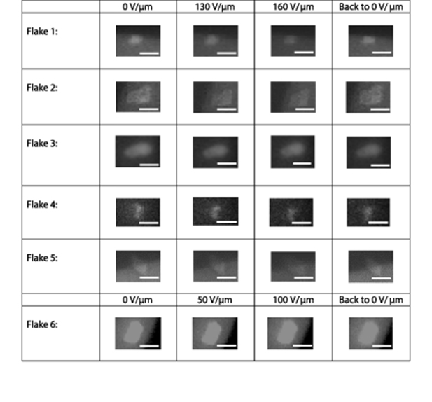 |
Similar to the bulk GO films, the fluorescence of each flake excited at 460 ± 25 nm and detected with 655 ± 25 nm filter experiences reduction with the applied electric field. A more substantial quenching observable on the level of individual flakes is induced by two orders of magnitude higher fields, while the low concentration of GO flakes deposited onto electrodes ensures a lower probability of a breakdown. Experiments with observed microamp or higher breakdown currents are not considered in this work, as irreversible optical changes could be potentially attributed to the effects of current-induced GO reduction.
The relative GO emission quenching and the reversibility of this effect is evaluated quantitatively, assessing the flake's fluorescence intensity normalized by that at 0 V throughout the experiment. Since the majority of the flakes have exhibited some alterations in the emission intensity with the applied electric field, six representative distinct and isolated flakes are analyzed here (figure 2). All six flakes exhibit an apparent gradual decrease in their emission intensity with the electric field (table 1), while flakes including flakes 1, 2 and 6 restore their intensity up to 100% ± 10% of the original as the field is removed. The most optimal intensity restoration is observed within one cycle. In further cycles some degree of fluorescence quenching starts to accumulate. The irreversible quenching of the flakes that do not show restoration or show only partial restoration can be attributed to several factors including submicroamp breakdown currents expected at high fields reducing GO flakes and/or creation of new charge traps and quenching defects. Thus, with removal of the electric field the fluorescence can be elevated due to clearing the charge traps, or permanently quenched due to GO reduction and new defect formation. For instance, although flakes 1 and 5 (figure 2) are experiencing a significant relative (up to 50%) and somewhat similar quenching, their restoration is markedly different as they could be either located in the different environments with sumbicroamp currents between neighboring flakes or electrodes occurring, or can be affected differently by the field as described above. The magnitude of the quenching for individual flakes can be above that observed in the bulk sample, in which the total effect is represented by the averaged response over the variety of flakes. This indicates a possibility to substantially alter GO optical properties on a single flake level. This effect will be further considered in the framework of the perturbation of excitonic behavior in GO under the influence of the electric fields including either exciton separation by the electric field or charge-transfer quenching originating from charges migrating in the field. The excitonic nature of fluorescence emission in GO has been recently explored by the K-edge x-ray absorption near edge structure measurements [27] and experiments involving excitation polarization dependence of the GO emission spectra [46]. Considering that GO fluorescence can be attributed to the excitonic process [14, 27, 30, 46], the separation of the electron and hole of the exciton with the electric field has the potential to decrease their recombination probability and, thus, induce GO fluorescence emission quenching up to even generating free charges. Additionally, the interaction of excitons with mobile charges in GO can also facilitate nonradiative exciton recombination. To assess the potential origin of the observed quenching effect, we develop a theoretical model of exciton separation by the electric field.
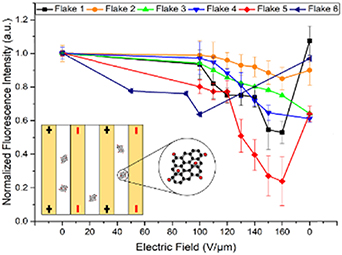
Figure 2. Normalized fluorescence intensity versus electric field strength for six individual GO flakes. Inset represents the schematic of GO flakes between IDE.
Download figure:
Standard image High-resolution imageIn this GO model, the effect of charged functional groups is considered negligible at an experimental pH value of 6, as only carboxyl groups that are present only at the edges of the flakes are charged (deprotonated at that pH) [47].
Additionally, exciton separation is expected to occur in the plane of GO flakes; thus, randomly distributed in-plane functional groups will yield in zero potential contribution. Based on the previous work [27], we consider the binding energy, effective mass, and Bohr radius of core excitons on GO surface as 350 meV, 0.196 mo and 6.23 Å, respectively. This allows approximating effective exciton potential energy in the electric field as

Where  is the potential energy of the exciton with dielectric constant
  as 2.31 for room temperature for GO and similar to that of PVP [27, 48].
  is the potential energy due to the maximum applied field. The electric field E acting upon electron and hole separated by the exciton radius r, yields a tilt in the excitonic potential energy well (figure 3).
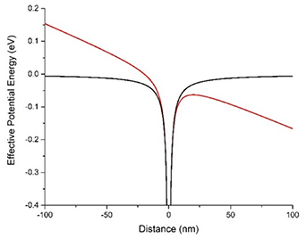
Figure 3. Calculated potential well of the exciton without (black line) and with (red line) applied electric field.
Download figure:
Standard image High-resolution imageThis increases the probability of electron tunneling out of the well preventing radiative exciton recombination and, therefore, quenching GO fluorescence. The probability of this event is assessed via the WKB approximation that will provide the rate of tunneling through a potential barrier [44].
Considering that no observable shifts were detected in GO emission spectra with the application of the electric field (figure 1), we expect the energy eigenvalues to remain the same. The change in the tunneling rates, however, is justified by the decrease in photoluminescence in the bulk GO film as well as within the individual flakes. The transmission probability in WKB approximation being proportional to the rate of tunneling will therefore represent the probability of separation of the electron-hole pairs affected by the electric field [44]:

Where  and
and  =
=  is the momentum of the electron in the well, E is the binding energy of exciton in GO, while r1 and r2 are the potential barrier's boundaries. The probability of electron escape from exciton per unit time is further calculated as
  , where v is the velocity of electron in graphene [18], r* is Bohr radius of exciton in GO [27]. Here we take into account the electron effective mass is approximately 20%–30% smaller than the hole effective mass in graphene [49].
As a result of this calculation, the maximum electric field of 1.6 V µm−1 applied to GO films yields a transmission probability of ∼5.2% for the bulk GO. This calculation accounts for the spectral integration time of 6 s increasing the number of exciton separation attempts and GO flake orientation to the electric field as exciton separation will be substantially less probable if they are perpendicular to each other. This theoretical prediction provides an estimate close to the experimental 6% quenching indicating a substantial role of electric field-induced exciton separation in GO fluorescence quenching. Although the process of exciton separation via the electric field is likely to contribute to fluorescence quenching, it still may not fully describe the intensity variation recorded in electric field experiments with bulk GO films as well as individual flakes. Other mechanisms adding to the exciton quenching may include such non-radiative pathways as charge defects/traps, phonon-assisted relaxation, and charge-induced quenching via charge-exciton interactions with charges formerly trapped and set in motion by the electric field.
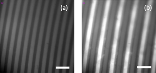
Considering the possibility of charge rearrangement in the GO flakes, we also explore the electrophoretic effects under the influence of the electric field. GO flakes subject to the fields from 0 to 6 V µm−1 in DI H2O suspension at high 1 mg ml−1 concentration exhibit substantial electrophoretic migration, which is indicative of flake charging and/or charge separation within the flakes. These charges can migrate and build up on the edges of GO flake or compensate positive-charged defects. Shortly after the application of the 6 V µm−1 electric field, GO flakes attach to the electrode of a single polarity, increasing the fluorescence signal from that electrode. The flakes stay attached even after the field is turned off, hence forming emissive aggregates on the electrode (figure 4). Prior to the electric field application, a minimal amount of emissive GO flakes is visible. After the field application, the GO flakes dispersed throughout and deposited onto the electrodes causing a substantial increase in the flakes' fluorescence emission at the electrodes; some individual GO flakes are still visible on top/surrounding the bright electrodes. The observed electrophoretic property suggests the possibility of directionally assembling nanoscale GO constructs via the electric field, benefiting several potential device applications. On account of the desirable high specific surface area, volumetric capacitance, energy and power densities, GO-coated nanodevices can be widely used as solid-state supercapacitors [47, 50–53]. GO deposition also allows for faster sensing and enhances sensitivity in bio and gas sensors [54, 55]. The vertical deposition of GO flakes may facilitate better electrolyte penetration and electron conductivity in solar cell systems [56, 57]. The multitude of the aforementioned applications suggests high potential of using electrophoretic deposition of GO described in this work for nanodevice fabrication and engineering.
Figure 4. Electrophoretic deposition of GO in aqueous suspension. Fluorescence images of GO flakes in DI water suspension on top of electrodes at (a) 0 V µm−1and (b) 6 V µm−1 where large numbers of flakes exhibit migration to the electrode of one sign. The scale bar length is 50 µm.
Download figure:
Standard image High-resolution image
4. Conclusion
This work explores the potential of using the simple mechanism of varying the electric field as a means of controlling the optoelectronic properties of GO. This mechanism is suitable for use in microelectronics and does not require complex and irreversible chemical functionalization. The effect of the electric field on GO fluorescence emission is studied both in bulk using a 1 mm GO film in PVP and on the microscopic level of individual GO flakes. For the GO incorporated in the PVP film, up to a 6% decrease in the fluorescence intensity is observed in the presence of 1.6 V µm−1 field. This effect appears to be reversible as GO emission intensity is increased at the cessation of the electric field. On the level of the individual flakes monitored via fluorescence microscopy between the interdigitated microelectrodes a similar trend is detected; however, more substantial observable changes are noted at markedly higher electric fields. With over 200 flakes studied, up to 50%–70%, fluorescence quenching is observed for some of the flakes, while a majority experienced smaller intensity variations. Upon field removal, the fluorescence intensity of a number of GO flakes are fully or partially restored; however, some have remained quenched potentially due to charge trapping or partial reduction via internal currents plausible at such field levels. The nature of the observed effect is described by the theoretical modeling of excitonic phenomena in GO flakes. The 5.2% probability of electrons escaping out of the exciton potential well calculated via WKB approximation provides a close estimate of the experimental quenching values and indicates a substantial role of exciton separation in the observed electric field quenching. This work, elucidating electric filed-induced changes in GO fluorescence, verifies the potential of utilizing the electric fields as a mechanism to fine-tune optoelectronic properties of GO with a degree of reversibility in device geometry. The electric field also provides a perspective mechanism for controlling the migration and location of GO flakes in aqueous suspension as they exhibit electrophoretic properties in aqueous suspension. This presents the potential of using electrophoresis to form microstructures and devices from GO flakes on the microscale.