

Abstract
Circular dichroism (CD) is widely used in biology, medicine, and physics. Three-dimensional (3D) chiral structures have been extensively studied because of their ability to produce significant CD effects. Previously reported 3D chiral structures are limited due to the complexity of fabrication processes and CD mechanisms. Here, spatially complementary chiral nanostructure (SCCN) arrays, which comprise bottom silver films with zigzag-shaped nanoslit and top complementary silver zigzag-shaped nanowires, are theoretically and experimentally shown to provide the CD effect. SCCN arrays are prepared experimentally by combining electron beam lithography (EBL) with normal electron beam deposition (NEBD) method and by utilizing EBL and NEBD only once. Numerical results demonstrate that localized surface plasmon excited on top complementary silver zigzag-shaped nanowires and surface plasmon polariton excited on bottom silver films with zigzag-shaped nanoslit result in the CD effect of SCCN arrays. In addition, the CD effect can be tuned by changing the width of the top complementary silver zigzag-shaped nanowires. Such type of chiral nanostructures has easy tunability, simple fabrication, and a better understanding of chiral optical response, which provides a new design for spatially chiral optoelectronic devices.
Export citation and abstract BibTeX RIS
1. Introduction
Chiral structure, which refers to the structure that lacking any mirror plane or inversion symmetry, exhibits different electromagnetic responses to the absorption and transmission of left circularly polarized (LCP) light and right circularly polarized (RCP) light [1–5]. Such different electromagnetic responses are usually represented by circular dichroism (CD) [6, 7]. CD measurements have been applied in optical filtering, selective thermal emission, and biological sensing [8–10]. However, natural chiral materials usually present an extremely weak CD effect due to the scale mismatch between the wavelength of circularly polarized lights and the molecule sizes. Artificial plasmonic nanostructures (APNs), which can manipulate light at a scale equal to or smaller than the wavelength of the incident light, can break the limitation to exhibit considerable CD effect.
In recent years, CD effects from planar chiral APNs, such as gammadion structures [11, 12], G-shaped structure [13], and S-shaped structure [14], have been studied. However, planar chiral APNs often have difficulty in generating a distinct CD effect due to the mirror symmetry in light propagation direction. To increase the CD effect of planar chiral APNs, various kinds of three-dimensional (3D) chiral APNs have been proposed [15–22]. The most typical type of 3D chiral APNs is helices, which include strict helix and structures that are arranged in helical ways using individual nanoparticles or nanorods; the CD effect of the former originates from the spiral current around the helix [15–17], while the CD effect of the latter is derived from localized surface plasmon (LSP) coupling between adjacent nanoparticles [18–20]. Another commonly used 3D chiral APN is stacked layers of the same planar unit cells, where the CD effect arises from LSP on different metal structures [21–25]. Although the two kinds of 3D chiral APNs can achieve considerable CD effects, a new type of 3D chiral APNs that can generate CD effects in different ways remains to be designed.
On the other hand, one of the major challenges of 3D chiral APNs is the preparation method. The traditional preparation methods of 3D chiral APNs are mainly divided into bottom-up and top-down methods. A typical method of the former is the molecular self-assembly method, which is usually utilized to fabricate helical metal nanoparticle assemblies [26, 27]. However, the flexibility of this method is severely limited due to the use of DNA, peptides, and cysteine as templates. The latter methods, which include laser direct writing (LDW), oblique angle deposition (OAD), polystyrene (PS) sphere template technology, electron beam lithography (EBL), are mostly used to manufacture stack layer structures [28–32]. However, each of the above-mentioned methods has its limitations to date. LDW cannot be used to prepare structures on nanoscale due to the diffraction limit of light. OAD usually needs to change the tilt angle many times, which results in complexity in the fabrication process. PS sphere template technology cannot produce structures with high resolution, and the stability of the prepared structure is difficult to control. EBL usually requires multiple alignment marks and the operation of the writing field. Thus, the manufacturing process of EBL is time consuming. The preparation method for multilayer structures also usually requires a combination of several previous methods. As a result, the preparation process involves multiple steps and is complex and time consuming. In order to overcome the fabrication difficulties, a new type of 3D chiral APNs with simple, flexible, and high-precision preparation method is highly required.
In this study, a novel design of spatially complementary chiral nanostructure (SCCN) arrays, which comprise bottom silver films with zigzag-shaped nanoslit and top complementary silver zigzag-shaped nanowires, is proposed and experimentally fabricated to realize the CD effect. Unlike traditional multilayer structures that require multiple EBL processes and metal deposition steps, the double-layer nanostructure is prepared experimentally by combining EBL with normal electron beam deposition method (NEBD) and by utilizing EBL and NEBD only once. This method simplifies the fabrication process. The experimental results show a good agreement with the simulated results in terms of the number of transmission peaks and the spectral shape of transmission and CD spectra. Numerical calculations show that the physical mechanisms behind the CD effects are LSP excited on top complementary silver zigzag-shaped nanowires and surface plasmon polariton (SPP) excited on bottom silver films with zigzag-shaped nanoslit. These results provide a way to generate CD effects using spatially complementary nanostructures and may lead to a gateway towards chiral manipulations of light. In addition, the CD effect is highly adjustable by changing the width of top complementary silver zigzag-shaped nanowires. This feature indicates the high tunability of the proposed chiral arrangement. The proposed SCCN has simple fabrication, easy tunability, and a better understanding of chiral optical response, which provides a new design for spatially chiral optoelectronic devices.
2. Design and fabrication of the SCCNs
It has been found that chiral response can be produced on the chiral metal nanowires or nanoslits due to their greater surface plasmon resonance and anisotropic nature. In order to combine the different properties that can produce chiral response, a simple method is to combine nanowires with nanoslits in a special organically way. Here, the proposed new design is to stack nanowires and nanoslits in a spatially complementary way. More specifically, the SCCN consists of a top silver nanowires, a polymethyl methacrylate (PMMA) space layer, a bottom silver films with nanoslits. Among them, the shapes of silver nanowires and silver films with nanoslits are complementary, and zigzag-shaped is selected as an example.
The fabrication process is schematically depicted in figure 1(a). It is shown that there are three main steps in the proposed fabrication method: The first step is to cover the PMMA layer of 270 nm thickness on the prepared ITO glass substrate by spin coating. In this step, it should be noted that ITO glass is prefabricated with deionized water, acetone and alcohol in advance and treated with ultrasonic. And the selected PMMA is AR-P 679.04; the second step is to expose the PMMA layer to zigzag-shaped pattern with periods of Px = 800 nm, Py = 600 nm by EBL method. In this process, a focused 10 KV electron beam controlled by the ELPHY Quantum (Raith) is used, which is equipped on the SEM (FEI Nova NanoSEM 450). Then the exposed samples were immersed in the developer and fixer for treatment. In this process, the developing time is one minute and the fixing time is 30 s; The third step is to deposit Ag with 60 nm on the sample by NEBD method. In this process, the E-beam evaporator (DE 400) is used to deposit Ag with the chamber pressure of ∼1 × 10⁻⁷ torr. The evaporation rate of the electron beam is 0.05 nm s−1. The Ag slugs with a purity of 99.99% are purchased from Alfa Aesar. After the three steps, SCCN arrays, which are composed of bottom silver films with zigzag-shaped nanoslit, top complementary silver zigzag-shaped nanowires, and dielectric layer PMMA, are fabricated. The inset is the unit cell of metal nanostructures and its related structural parameters. Px and Py are the periods along the x- and y-axes directions of bottom silver films with zigzag-shaped nanoslit, respectively. w is the width of top complementary silver zigzag-shaped nanowires. h is the thickness of dielectric layer PMMA. t represents the thickness of bottom silver films with zigzag-shaped nanoslit and top complementary silver zigzag-shaped nanowires. l1, l2 and  are the lengths of the two parts of the nanowire and the angle between them, respectively. In our manuscript, we fix l1 = 200
 nm, l2 = 200
 nm and
  = 108.4°. It is clear that the preparation process of the proposed SCCN arrays reduces the need for multiple EBL processes and metal deposition steps for multilayers nanostructures [32], which greatly simplifies the manufacturing process and reduces time and costs. Figure 1(b) depicts a top view scanning electron microscopy image of the final fabricated SCCN arrays.
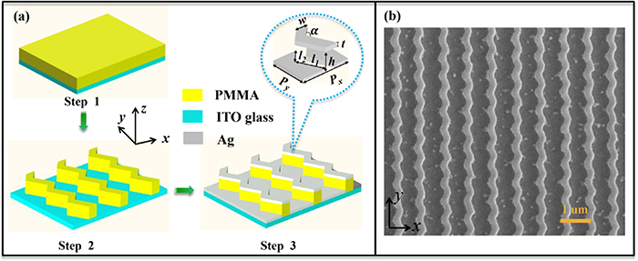
Figure 1. (a) Schematic of the fabrication process of SCCN arrays. Step 1: PMMA is spin-coated onto ITO glass; step 2: the template is exposed by EBL; step 3: silver is deposited by NEBD method. The inset shows the configuration of the unit cell of metal nanostructures. (b) SEM image of fabricated SCCN arrays.
Download figure:
Standard image High-resolution image3. Results and discussion
The transmission and CD spectra of SCCN arrays are characterized by self-built experimental equipment (detailed in the Methods section) in figures 2(b) and (d). Simulated transmission and CD spectra of SCCN arrays are also investigated by the finite element method in figures 2(a) and (c). Figure 2(a) shows three obvious transmission peaks at around 850 nm, 810 nm, and 760 nm, which are denoted as Modes I, II, and III, respectively. At Mode I, the transmittance of LCP light is greater than that of RCP light. Meanwhile, the transmission of LCP light is strong and the transmission of RCP light is weak at Mode III. As a direct result of this phenomenon, reversed CD spectral shape appears in figure 2(c). Experimentally measured transmission results in figure 2(b) confirm the presence of three resonant modes at 960 nm, 860 nm, and 760 nm. Figure 2(d) also shows the experimentally measured CD result, which confirms the existence of the reversed CD spectral shape. Therefore, the experimental results are basically consistent with the simulation results in terms of the number of transmission peaks and the spectral shape of transmission and CD spectra. In addition, experimentally measured spectra are slightly red-shifted compared with the simulated spectra. This result can be explained by the influence of PMMA and substrate in the experiment.
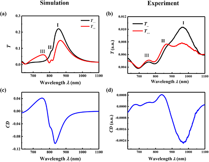
Figure 2. (a) Simulated and (b) experimental results of transmission spectra under LCP and RCP illumination, and CD spectra for (c) simulated and (d) experimental results.
Download figure:
Standard image High-resolution imageTo unveil the physical mechanism of the CD effect, the surface current distributions of SCCN arrays in the x-y section are calculated in figure 3. The red and blue parts represent the positive and negative charges, respectively.

Figure 3. Simulated charge distribution of SCCN arrays at different resonant modes.
Download figure:
Standard image High-resolution imageIn Mode I [figures 3(a) and (b)], the red and blue charges are mainly spaced horizontally on the lower silver film, which implies that the SPP is arranged horizontally on the lower films. In Mode II [figures 3(c) and (d)], the red and blue charges are mainly concentrated on the ends of the upper nanowires, which indicates that the LSP is excited on the upper nanowires. Notably, the combination way between the LSP on the upper nanowires and the oscillation on the lower films differs under different circularly polarized light illumination. Under the LCP illumination case, the oscillations on the lower films are distributed on the two sides of the right-facing rods that comprise the upper nanowires. While oscillations on the lower films under the RCP illumination case are distributed on the two sides of the corners that comprise the upper nanowires. The difference in the combination way between the resonance of upper nanowires and the lower films produces the CD effect. In Mode III [figures 3(e) and (f)], the red and blue charges are spaced vertically on the bottom silver films, which implies that the SPP is arranged vertically on the lower films. Notably, the oscillation direction of SPP differs under different circularly polarized light illumination. Under the LCP illumination case, the oscillations on the lower films are from the top-left corner to the bottom-right corner. By contrast, the oscillations on the bottom silver films under the RCP illumination case are from the top-right corner to the bottom-left corner. Overall, the resonant modes of SCCN arrays combine the resonance of the top nanowires and the bottom nanofilms with nonoslits in a spatially complementary manner, which provides a new method of generating CD and can help deepen the understanding of the chiral response.
On the basis of the above-mentioned analysis, parameters of upper nanowires and lower films are varied systematically to investigate the effect of structural parameters on the CD characteristics of SCCN arrays. Firstly, the influence of the width of the top complementary silver zigzag-shaped nanowires on the CD effect is studied. As shown in figure 4, w is increased from 180 nm to 220 nm while other parameters are kept unchanged. It can be clearly seen that with the increase in w, Modes I and III exhibit obvious blue shift, and Mode II also exhibits blue shift. The reason is that the increase in the width of the upper nanowires will increase the width of the nanoslit and then reduce the length of lower films, which results in the shortening of the oscillating path of SPP on lower films. This condition will eventually cause the blue shift of Modes I and III. As for Mode II, considering the transverse diameter ratio of the upper nanowires, the increase in width of upper nanowires will shorten the oscillating path of the LSP on the upper nanowires. This shortening will cause the blue shift of Mode II.
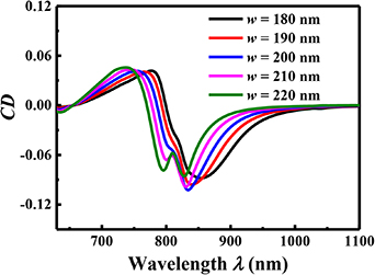
Figure 4. Simulated CD spectra of SCCN arrays with different w values.
Download figure:
Standard image High-resolution imageThen the influence of the periods of the lower films on the CD effect is studied. As shown in figure 5, the periods of the SCCN arrays are systematically varied. Figure 5(a) shows that, as Px increases from 780 nm to 820 nm, Modes I and II show significant red shift, and Mode III barely moves. For Mode I, the increase in the length of the lower film will increase the propagation paths of SPP in the horizontal direction, which will cause the red shift of Mode I. For Mode II, the increase in the length of the lower film will reduce the width of upper nanowires, which will increase the length of the upper nanowire. This increase will result in the elongation of the oscillation path of LSP on the upper nanowires, which will eventually cause the red shift of Mode II. For Mode III, the increase in the length of the lower film barely affects the oscillation path of SPP in the vertical direction. As a result, Mode III barely moves.

Figure 5. Simulated CD spectra of SCCN arrays with different (a) Px values, and (b) Py values.
Download figure:
Standard image High-resolution imageSimilarly, figure 5(b) shows that, as Py increases from 580 nm to 620 nm, Modes II and III show significant red shift, and Mode I barely moves. For Mode I, the increase in the width of the lower film barely affects the oscillation path of SPP in the horizontal direction. Thus, Mode I barely moves. For Mode II, the increase in the width of the lower film will reduce the width of the upper nanowires. This reduction will increase the length of the upper nanowire. As a result, the oscillation path of LSP on the upper nanowires elongates. This condition will eventually cause the red shift of Mode II. For Mode III, the increase in the width of the lower film will increase the propagation paths of SPP in the vertical direction, which will cause the red shift of Mode III.
The above-mentioned results combined with figures 4 and 5 indicate that the CD effect of SCCN arrays can be flexibly regulated by adjusting the parameters of the upper nanowires and the lower films. In addition, the width of upper nanowires greatly affects the CD effect SCCN arrays compared with the periods of the lower films. This phenomenon proves the easy tunability of SCCN arrays.
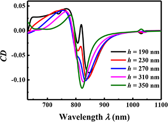
The influence of the thickness of the dielectric layer on the CD effect is finally studied. As shown in figure 6, h is increased from 190 nm to 350 nm while other parameters are kept unchanged. With the increase in h, Mode I exhibits obvious blue shift. As the thickness of the dielectric layer increases in the z-direction, the length of the lower film decreases in the x-y direction. This condition results in the shortening of the oscillation path of SPP in the horizontal direction. Notably, the intensity of Mode I increases significantly with the increase in h, which provides an idea for enhancing the CD effect.
Figure 6. Simulated CD spectra of SCCN arrays with different h values.
Download figure:
Standard image High-resolution image
4. Conclusions
In summary, a novel design of SCCN arrays, which comprise bottom silver films with zigzag-shaped nanoslit, a PMMA layer and top complementary silver zigzag-shaped nanowires, is demonstrated numerically and experimentally to realize the CD effect at the visible and near infrared region. The spatially complementary nanostructure is prepared experimentally by combining EBL with NEBD and by utilizing EBL and NEBD only once. This method simplifies the fabrication process. The results show that the physical mechanisms behind the CD effect are LSP excited on top complementary silver zigzag-shaped nanowires and SPP excited on bottom silver films with zigzag-shaped nanoslit. This unique combination way between the resonance of top nanowires and the bottom films provides a new way to generate CD effects using spatially complementary nanostructures and may lead to a gateway towards chiral manipulations of light. Moreover, the CD effect can be highly tuned by changing the width of nanowires. Spatially complementary structures with other chiral shapes can also be prepared in the proposed way to produce similar effects. The proposed SCCNs is of advantages of easy tunability, simple fabrication, and a better understanding of chiral optical response, which provides a new design for spatially chiral optoelectronic devices.
5. Methods
5.1. Simulation
The transmission and CD properties of the proposed structures can be simulated by the finite element method (COMSOL Multiphysics 5.3). The periodic boundary conditions are applied to the x-z and y-z planes, and two perfectly matched layers are located at the bottom and top along the z direction. The dielectric properties of Ag can be derived from the experimental data of Johnson and Christy [33]. The relevant parameters used in the simulation of figures 2 (a) and (c) are: Px = 800 nm, Py = 600 nm, w = 400 nm, t = 60 nm, h = 270 nm. The transmission spectra of LCP light and RCP light are represented by T−− and T++, respectively. The CD effect can be defined as the difference in the transmittance of RCP and LCP light, that is, CD = T++ − T −−.
5.2. Optical measurements
Transmission spectra of the fabricated SCCN arrays were obtained by self-built experimental equipment. Broadband white light output from lens passes through the linear polarizer (Thorlabs, WP25M-UB) and quarter wave plate (Thorlabs, AQWP05M) to produce LCP or RCP light. The transmitted light from the sample is then collected by the objective lens (Thorlabs, MY100X-806). The reflector (Thorlabs, PF10-03-F01) is used to reflect light to the CCD (Lambrt Instruments, TRiCAM G 2n) to display an enlarged image of the sample. The reflector is also used to transmit light, which is then passed through the lens to the spectrometer system for transmission spectroscopy. CD spectrum is calculated by the difference of transmission spectrum under LCP and RCP light.
Acknowledgments
This work was supported by the National Natural Science Foundation of China (Grant No. 61575117); Fundamental Research Funds for the Central Universities (Grant No. GK201601008); Fundamental Research Funds for the Central Universities (Grant No.2019TS122).
Conflict of interest
The authors declare no conflict of interest.