
Abstract
A nanostructured transparent electrode with high average visible transmittance of 76%, low sheet resistance of 7.0 Ω/sq and steep transmittance drop in the near-infrared (NIR) range is investigated by simulations and experiments. The electrode is composed of a nanostructured substrate, on which a trilayer, consisting of an ultrathin 14 nm thick silver film embedded between thin films of TiO2 and Al-doped ZnO, is deposited. Directional silver deposition results in the formation of a disk-hole array without additional lift-off or etching steps. While the trilayer approach enables increased visible transmittance, the transmittance in the NIR regime is decreased by a broadband plasmonic dipole excitation in the disk-hole array. Moreover, a rich mode spectrum of weaker multipole surface plasmon excitations is observed in the nanodisk- and nanohole array. The presented electrode holds great potential for applications in optoelectronic devices, solar control coatings and solar cells.
Export citation and abstract BibTeX RIS

Original content from this work may be used under the terms of the Creative Commons Attribution 3.0 licence. Any further distribution of this work must maintain attribution to the author(s) and the title of the work, journal citation and DOI.
1. Introduction
Transparent electrodes combine high visible transmittance with high conductivity and are an essential component of modern optoelectronic devices (e.g. touchscreens, flat-screens, electrochromic displays, light-emitting diodes), low-emissivity (low-e) glass coatings and solar cells [1, 2]. Various families of transparent electrodes are present today, most prominently (i) transparent conductive oxides (ii) ultrathin metals and (iii) (nano)structured metals. The most commonly used conductive oxide is tin-doped indium oxide (ITO) with low resistivity and high optical transmittance [3]. Disadvantages of ITO lie in the high price and scarcity of indium, as well as the limited applicability in flexible devices due to its brittleness [4]. Other common conductive oxides are aluminum-doped zinc oxide (AZO) and fluorine-doped tin oxide (FTO), with the latter being widely used in low-e glass coatings. Ultrathin metals (gold, silver, copper) with thicknesses around 5–15 nm, embedded between two dielectric materials, offer an attractive alternative with low sheet resistance down to 6 Ω/sq and highest transmittance above 90% in the visible range [5]. The high conductivity is owed to the metal, while the dielectrics allow sufficient suppression of reflectance of the metal, hence the high transmittance [6]. These types of electrodes are already established as coatings in the glass industry for solar control and low-e coatings [7]. Low-e coatings are typically composed of three layers (trilayer) with one silver (Ag) layer between two dielectrics [8], while more advanced solar control coatings with better filter properties are made of more than 10 planar layers with several metal and dielectric layers [2].
Structured metal-based electrodes mainly employ the concept of a nanowire network design and can be achieved by random assembly of metal nanowires on a substrate from solution [9], or periodically, by lithography or printing techniques. Examples for periodic structures include nanohole arrays [10–12], one-dimensional nanowire gratings [13, 14] and two-dimensional nanowire networks [15]. Although these periodic structures show attractive optical and electrical properties, fabrication, especially of submicron structures, involves tedious processes, such as ion etching, electron beam lithography and lift-off steps, which are difficult to adapt to high-throughput methods. Transparent electrodes made of metallic nanostructures in the submicron range allow for excitation of localized surface plasmons and propagating surface plasmon polaritons (SPPs) [15]. In the vicinity of the surface plasmon resonance, the extinction cross-section can become several times larger than the actual geometric size of the structures, which is associated with increased scattering and absorption. In light management schemes for solar cells, such effects can assist in concentrating the electric fields in certain regions or scatter the light to increase the path length in the active material [16, 17]. However, in applications where maximum direct light transmittance is crucial, the excitation of surface plasmons can lower the performance. Yet, extraordinary optical transmission (EOT) observed in optically thick metallic nanohole arrays showed strongly enhanced narrow band transmission owing to plasmon excitations [18]. Consequently, a careful design of plasmonic nanostructures is essential to achieve the desired optical performance. Materials employed for plasmonic applications encompass metals, metal alloys and doped semiconductors [19]. In addition to these materials, graphene has been studied intensively in the last years as plasmonic material [20–23]. Among the metals, Ag exhibits the lowest optical losses in the visible and the near-infrared (NIR) range [19] and is therefore the metal of choice in this study.
The nanostructure introduced in this work is a combination of the two aforementioned concepts. Firstly, an ultrathin metal layer is embedded between two dielectrics to increase transmittance in the visible range. The metal layer is nanostructured to increase the NIR reflectance and absorption compared to a planar electrode, through the excitation of surface plasmons. Particular attention is directed to the ease of upscalability of the design. Therefore, nanoimprint lithography (NIL) without further lift-off processes is proposed, as reported for plasmonic color filters [24, 25]. The aspect ratio is kept at a minimum to avoid complications for the potential application in optoelectronic devices. The proposed nanostructure is thoroughly analyzed by optical simulations of transmittance, charge density and electric field enhancement to study the origin of the plasmonic modes. Such multifunctional transparent electrodes can have various applications, such as solar control coatings, solar cell front-contacts that reflect the solar spectrum below the band edge to reduce the temperature of the cell and in displays to decrease heating due to NIR-radiation.
2. Methods
2.1. Simulation
Optical simulations are based on finite-difference time-domain (FDTD) method (commercial software: FDTD Solutions, Version 8.7.4 from Lumerical Solutions, Inc., Canada). The complex refractive indices of Ag and glass were taken from literature [26]. The resist was assumed to have the same refractive index as glass. The complex refractive indices of titanium dioxide (TiO2) and AZO were derived from transmittance T and reflectance R measurements of respective planar thin films by a transfer matrix algorithm [27, 28]. The experimental complex refractive indices of Ag, TiO2 and AZO together with a multi-coefficient fit of the data, used in the FDTD simulation, can be found in the supporting information (figure S1 is available online at stacks.iop.org/NANO/30/265201/mmedia). Transmittance and reflectance spectra of the periodic nanostructure, as well as electric field maps for normal incident light (incident from the air medium) are simulated with a single unit cell with periodic boundary conditions in x- and y-direction and 16 layers of perfectly matched layers (PMLs) in z-direction. The unit cell dimensions are 400 nm in x- and y-direction and 1000 nm in z-direction. A broadband plane wave light source is used and physical properties are analyzed in the wavelength range from 400 to 2000 nm. The mesh was chosen to be uniform in x-, y- and z-direction with a mesh size of 1 nm and a time step of 0.0019 fs. In the electric field maps ∣E/E0∣, the electric field E is normalized to the incident field E0. For the angle wavelength map, Bloch-periodic boundary conditions were taken instead of period boundaries and a mesh of 5 nm was chosen to reduce simulation time. Surface charge density at the Ag surface was calculated from the divergence of the electric field. Simulations of absorption and scattering efficiency of the single isolated nanodisk and nanocross have been performed in homogeneous refractive index environment (n = 1.0 and n = 1.45, respectively) and a total-field scattered-field source (implemented in Lumerical—FDTD solutions) was used. PMLs were placed in x-, y- and z-direction and a uniform mesh of 1 nm was employed.
2.2. Nanoimprint lithography
A silicon (Si) master template with pillars (period 400 nm, height 40 nm and diameter 300 nm) was obtained from EULITHA AG (Switzerland) with structured area of 5 mm × 5 mm. Polydimethylsiloxane (PDMS) (Sylgard 184, The Dow Chemical Company, USA, distributed by Sigma Aldrich Handels GmbH, Austria) was cast over the Si-master und cured overnight at 60 °C to achieve a PDMS working stamp. UV-resist (Amonil MMS 10, AMO GmbH, Germany) was spincoated for 120 s at 3000 rpm on cleaned soda-lime glass substrates and the PDMS stamp was placed subsequently on top without additional pressure. UV curing of the resist was done with a UV lamp (Bio-Link 365, Vilber Lourmat, France) at λ = 365 nm with an irradiation dose of 10 J cm−2. Detaching the PDMS stamp from the cured resist results in a copy of the original master structure.
2.3. Material deposition
Films of TiO2 and AZO were deposited by direct current magnetron sputtering system (Leybold Univex 450 C, 3SC Leybold Germany) with base pressure of 1.9–7.0 × 10⁻⁸ mbar. TiO2 was deposited from a 4 in titanium (Ti) target by reactive sputtering in argon (Ar)/oxygen (O2) (80/20 ratio) atmosphere at 120 W sputter power and 1.0 × 10⁻³ mbar gas pressure, resulting in a sputter rate of 0.015 nm s−1. AZO was deposited in pure Ar atmosphere at pressure of 1.0 × 10⁻³ mbar and sputter power of 120 W from a 4 in target composed of zinc oxide (ZnO) and 2 wt% aluminum oxide (Al2O3) yielding a sputter rate of 0.53 nm s−1. Ag was deposited in a Leybold Univex 450 evaporation system (from 3SC Leybold Germany) by thermal evaporation with base pressure 4 × 10⁻⁷ mbar. Ag granules were purchased from MaTeck GmbH (Germany) with 99.9999% purity. Substrates were placed 30 cm vertically above the evaporation source. A high evaporation rate of 1.1 nm s−1 was chosen to improve film continuity and reduce optical losses, as reported in literature [29, 30]. Furthermore, substrates with TiO2 have been modified with (3-aminopropyl)trimethoxysilane (APTMS) to further foster continuous film growth, with protocol taken from literature [30]. Morphological characterization of Ag films on glass and glass/TiO2 substrates, with and without APTMS-treatment, can be found in the supporting information (figure S2).
2.4. Characterization
Optical measurements were performed with a Bruker Vertex 70 Fourier-transform infrared spectrometer, equipped with additional visible light source. All measurements were done with unpolarized light. Zero-order transmittance measurements were referenced to air and the beam was incident on the coated side of the sample. Zero-order reflectance measurements were done with the A513QA accessory of the spectrometer, at 15° angle of incidence, with beam incident on the coated side of the sample. The reflectance signal was referenced to calibrated mirror (STAN-SSH-NIST, Ocean Optics, USA) in the range from λ = 350 nm to λ = 2350 nm and to optically thick gold mirror from λ = 2350 nm to λ = 25 000 nm. The characterization of nanostructured and planar trilayer was done on the same sample to ensure consistency in material thicknesses. Atomic force microscopy (Molecular Imaging, USA) was performed in tapping mode with PPP-NCHR (NANOSENSORSTM, Switzerland) tips. Scanning electron microscopy (SEM) (SUPRA 40, Carl Zeiss Microscopy GmbH, Germany) imaging was done at 5 kV acceleration voltage with an in-lens detector. Measurement of sheet resistance was done by four-point, in-line probe technique (Süss MicroTec, Germany probes, connected to an Agilent 4156 C semiconductor parameter analyzer from Agilent Technologies, Inc., USA).
3. Results and discussion
The proposed nanostructured transparent electrode design for high transmittance in the visible wavelength range and high reflectance in the NIR, is shown in figure 1(a). The design consists of a nanostructured resist with periodic posts, period Λ = 400 nm, diameter D = 300 nm and height h = 40 nm, and subsequent depositions of TiO2, Ag and AZO. The deposition of the trilayer on top of the nanostructured substrate results in separated Ag disks on top of the posts and Ag nanohole array below. TiO2 and AZO are shown to be very efficient materials in such trilayer systems due to their optical [5, 6] and adhesion [31] properties. The Ag thickness of 14 nm was determined from experiments as the lowest thickness at which a continuous, defect-free Ag film can be achieved by thermal evaporation and was therefore used in simulation and experimental works. To achieve maximum transmittance in the visible range from λ = 400 nm to λ = 700 nm, the thicknesses of the TiO2 layer and the AZO-layer were varied in a transfer matrix algorithm for a planar multilayer system, as described previously [32], excluding the impact of the nanostructure. High transmittance values close to maximum are achieved for TiO2 thickness of 27 nm and AZO thickness of 51 nm, evident from the complete parameter scan found in the supporting information (figure S3). The simulated transmittance and reflectance spectra of the nanostructured trilayer are shown in figure 1(b). The spectra of the nanostructure show several resonances in the visible and NIR range with the most significant at around λ = 1450 nm with transmittance down to 0.5% and reflectance up to 86%. In the visible range (from λ = 400 to 700 nm), the average transmittance is around 82%, while the reflectance is close to 0% from λ = 400 to 600 nm, confirming the suitability of the TiO2 and AZO thicknesses. For comparison, a single planar Ag layer with the same thickness on glass is presented, that shows significantly lower transmittance in the visible and shallow decrease of transmittance in the NIR range.

Figure 1. (a) Schematic illustration of the investigated nanostructure with additional cut planes for clarification of the layer structure. (b) Simulated transmittance and reflectance spectra of the nanostructured electrode (black solid and dashed line). The transmittance spectrum of a single Ag layer on glass with the same thickness is shown for comparison (gray solid line).
Download figure:
Standard image High-resolution imageTo elucidate the origin of the diverse resonances in the spectrum, the structure was decomposed into its main components, namely a disk array and a hole array and the results are shown in figures 2(a), (b). In addition to the transmittance spectra, the surface charge density at the upper Ag/AZO interface, as well as the electric field enhancement ∣E/E0∣ are shown. The disk array shows a pronounced in-plane dipole mode with transmittance dropping down to 2% at λ = 1170 nm. Reasons for the occurrence of the dipole mode at a relatively high wavelength are the large diameter of the disks [33], the small thickness of the Ag and the embedding of the metal disks in high refractive index materials [34, 35]. In addition to the dipole mode, higher order multipole excitations can be clearly distinguished in the visible wavelength range. Higher order multipolar plasmon excitations have been observed for a wide variety of geometries such as spherical particles [36], nanorods [37], nanotriangles [38], disks [33, 39] and shell particles [40], when the dimensions of the particles are sufficiently large. The charge density of the multipole modes of the disks can be assigned with a (m, n)-notation with m being the number of radial node lines and n being the circular node lines as mentioned in Schmidt et al [41]. The (1, 1) and (1,2)-modes are less pronounced and with a smaller spectral width than the dipole mode, as generally mentioned for higher order multipoles in literature [42]. Let us note that even higher order modes (1, 3) and (1, 4) at λ = 545 nm and λ = 515 nm, respectively, are present, but with very faint signatures in transmittance. The absorption and scattering efficiency of a single isolated disk in air with otherwise same parameters (see figure S4 in supporting information) exhibits the multipole modes at roughly the same spectral positions (λmultipole-mode ± 30 nm) compared to the disk array arrangement. Therefore, interaction between the disks in array configuration by near-field [43] or diffractive coupling [44–46] can be assumed to be small. Further, in the multipole modes absorption of light is dominant compared to scattering, while in the dipole mode scattering outweighs absorption.
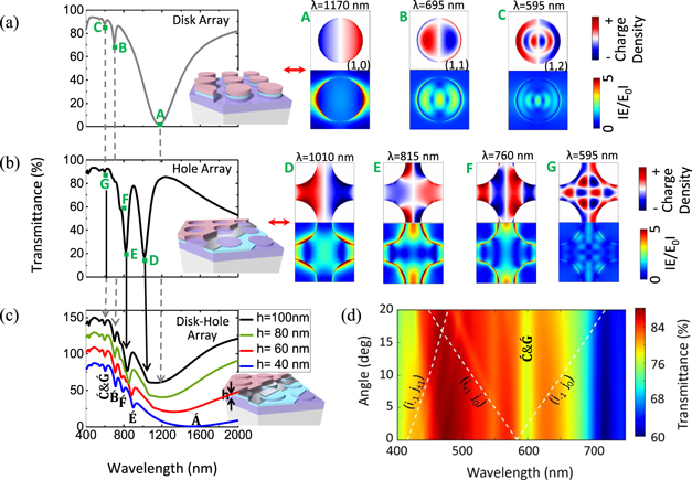
Figure 2. Simulated transmittance spectra of (a) disk array and (b) hole array with respective surface charge density (scale adjusted for each image for better visibility) and electric field enhancement ∣E/E0∣ at the Ag/AZO interface. The electric field polarization of the incident light is indicated by the red double arrows. (c) Transmittance spectra of disk-hole array for different height values. An offset is introduced for better distinction between the spectra of differing heights. (d) Angle-wavelength map of the disk-hole array structure with h = 40 nm and TM polarization. Theoretical dispersion of Rayleigh–Wood anomalies with various diffraction orders (i, j) are presented for glass (white dashed lines).
Download figure:
Standard image High-resolution imageThe hole array shows several spectral features in transmittance (designated (D)–(G)) which will be explained in detail in the following. A metallic hole array supports the excitation of SPPs, due to the grating vector of the array that allows the wavevector of the incident light to match to the wavevector of the SPPs [47]. The SPPs can be excited on either side of a metallic film and coupling to symmetric and antisymmetric modes is observed when the metal film thickness is reduced [48]. These propagating modes on very thin metal films can only be excited when the supporting substrate and the superstrate do not differ too much in their refractive indices [49, 50]. The structure presented in this work shows significant differences in the refractive indices as the substrate is glass and the superstrate is air. Additional refractive index differences are caused by the embedding of the Ag-film between TiO2 and AZO. The efficient excitation of propagating plasmon modes seems therefore unlikely in this system. To confirm this assumption, further simulations with different angles of incidence with transverse magnetic (TM) and transverse electric (TE) polarization have been performed (not shown here) that do not indicate any significant angular dependence and therefore suggest that the observed plasmon modes are of localized nature. The representation of the unit cell of the hole array as a cross (see figure 2(b)) is rather unusual but represents the origin of the localized modes. It can be shown, that the modes of the array can be traced back to a single isolated cross with otherwise same structural parameters, showing strikingly similar charge densities and spectral positions (see figure S5 in supporting information). The main difference between the hole array (cross array) and the isolated cross is the presence of two additional charge poles at the horizontal tips (along the electric field polarization) of the isolated cross, which are otherwise not found in the hole array arrangement. The charge density of the hole array is presented for several multipole excitations [51] with (D) and (E) being the most prominent. The plasmon mode (F) is hardly noticeable, as being superimposed with (E). Additionally, several weak modes can be observed in the visible range (charge density only shown for (G)). Interestingly, no hole dipole mode, which would exhibit two poles at the short rim between two holes along the incident electric field polarization [24, 52], is observed in the investigated wavelength range. The effect of extraordinary transmission observed in subwavelength apertures in metal films is associated with increased transmittance, compared to a purely geometric consideration of the coverage of a substrate by metal apertures [11, 18]. To assess whether EOT plays a role in the high visible transmittance of the hole array, a simple model is developed. The fraction of the area covered by holes fh and therefore free of metal can be given by fh = (π·D2)/(4·Λ2). A purely geometric consideration of total transmittance Tg(λ) of a hole array yields Tg(λ) = fh·Tr(λ) + (1−fh)·Tt(λ), with Tr(λ) and Tt(λ) being the simulated transmittance of a single planar air/resist interface and a planar trilayer of an Ag-film between TiO2 and AZO, respectively. Comparing the simulated hole array transmittance of figure 2(b) with Tg(λ) (see figure S6 in supporting information), indicates although a minute increase at certain wavelength in the visible is observed, the overall visible transmittance is lowered. Contrarily, the transmittance of the hole array for wavelength greater than 1100 nm is significantly higher than Tg(λ).
To investigate the impact of coupling between the disk- and the hole array, the height was gradually decreased (see figure 2(c)) as means to increase interaction. For a height of h = 100 nm, the spectral mode positions agree very well with the individual disk- and hole array. By decreasing the height, the disk dipole mode (A) is shifted to higher wavelengths and is significantly broadened by the coupling of the dipole charge distribution in the disk and the induced image charges in the hole array [53, 54]. The hole mode (D) is further merged with the disk dipole mode and becomes indistinguishable. This behavior of merging disk and hole modes is contrary to a recent study with similar geometry, where a dipole hole mode and a dipole disk mode formed hybrid states. These hybrid states showed increased energy splitting when the disks and holes were brought in closer proximity [24]. A possible explanation for this discrepancy could be, that the hole mode in the present study has no dipole character. The hole mode (E) is shifted to slightly higher wavelength upon decrease in height, lifting the superposition with the hole mode (F) and therefore, a clear additional transmittance minimum ( ) can be observed in the disk-hole array. The modes below λ = 800 nm originating from the disk- and hole array remain at the same spectral positions. A variation in Ag layer thickness, while keeping the rest of the structure parameters of the disk-hole array unaltered, leads to a red-shift of the discussed plasmon modes for decreased Ag thickness and a blueshift when the Ag thickness is increased. Furthermore, the transmission of the electrode is higher the thinner the Ag layer (see figure S7 in supporting information). The simulation of the angle-wavelength map in the visible range shown in figure 2(d) confirms the localized nature of the identified higher order surface plasmon modes by angle independence, hence, indicating non-diffractively coupled modes [55]. In addition to the already discussed localized plasmon modes in the disk- and hole array, faint inclined branches with spectral position shortly below λ = 600 nm and around λ = 450 nm (for 0° incidence angle) can be observed. A possible explanation for the branches could be Rayleigh–Wood anomalies as observed when a diffraction order (i, j) becomes parallel to the grating plane. Rayleigh–Wood anomalies are only dependent on the grating period and the medium in which the grating is embedded (in this study glass and air) [47, 56]. As the theoretical dispersion [47, 56] (white dashed lines in figure 2(d) for glass) does not match with the observed branches, Rayleigh–Wood anomalies can be ruled out as explanation. Consequently, the branches must originate from grating coupled waveguide modes [57] in the trilayer. Additional simulations (data not shown) indicate that these modes are present at roughly the same spectral positions for a situation when the Ag is omitted with the rest of the structure unaltered.
Experimental realization of the proposed nanostructure is done by nanostructuring a UV-resist on a glass substrate with NIL (stuctured area of 5 mm × 5 mm) and subsequent deposition of the trilayer. While the dielectric layers TiO2 and AZO were deposited by magnetron sputtering, the Ag layer was deposited by thermal evaporation. Thermal evaporation ensures directional deposition of the metal and consequently results in well separated Ag disks and holes without metal deposits on the flanks of the posts. A SEM image of the transparent electrode without AZO top layer (figure 3(a)) exhibits a thin dark line around the edges of the elevated disks, confirming good separation between disks and holes. Further, occasional defects are observed in the otherwise continuous Ag film. Characterization by AFM revealed the height of the disks to be h = 45 nm, as shown in figure 3(b).
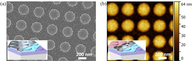
Figure 3. (a) SEM image of the nanostructured transparent electrode without AZO top layer (see inset for schematic). (b) AFM image of the structure with AZO top layer (see inset for schematic).
Download figure:
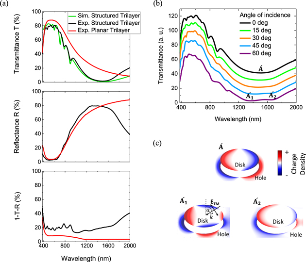
Standard image High-resolution imageMeasured zero-order transmittance and reflectance spectra of the planar and nanostructured trilayer together with the simulated transmittance spectrum of the nanostructure can be found in figure 4(a). The simulation was additionally corrected for the air/glass-interface of the non-coated side of the substrate, which is otherwise not included in the simulation [32]. Here, only the zero-order transmittance of the simulation is presented, which leads to a small reduction of app. 1% below λ = 585 nm compared to simulated transmittance of all diffraction orders. These corrections allow for a direct comparison of the experiment and the simulation. The experimentally observed spectral positions of the modes in the NIR agree well with the simulation, while the modes in the visible are slightly shifted. The nanostructured trilayer shows an average transmittance of 76% in the visible range which is lower compared to the planar trilayer, but in return has a steeper transmittance drop in the NIR and reaches a minimum of 1.5% at λ = 1500 nm. For wavelength greater than λ = 1800 nm, the transmittance of the nanostructured transparent electrode exceeds that of the planar trilayer. Considering applications in solar control coatings, this behavior is not so crucial as the solar spectral irradiance above λ = 1800 nm contributes only app. 4% of the total solar energy (see figure S8 in supporting information). The transmittance and reflectance spectra for wavelengths above λ = 2000 nm, which is of interest for applications in low-e coatings, can be found in the supporting information (figure S9). Let us note that an increase in transmittance at higher wavelength (above λ = 2000 nm) can be even favorable in situations where thermal radiation from a heated surface is desired to be emitted into the surrounding environment.
Figure 4. (a) Experimental (Exp.) transmittance, reflectance and 1 − T − R spectra of the planar and nanostructured trilayer. Additionally, the simulated (Sim.) transmittance spectrum of the nanostructured trilayer is presented. (b) Experimental transmittance spectra at different angles of incidence with unpolarized light. An offset of the individual spectra is given for better distinction. (c) Simulated charge density on the Ag surface of the disk-hole array at marked spectral positions at 0° and 60° incidence angle with TM polarization.
Download figure:
Standard image High-resolution image
The low reflectance values of the planar and nanostructured trilayer in the visible range confirm the correct design and deposition of the TiO2 and AZO layer. The nanostructure exhibits a higher reflectance between λ = 720 nm and λ = 1460 nm compared to the planar trilayer, indicating that the lower transmittance in this range is due to increased reflectance and absorption. In addition, the 1 − T − R spectrum, accounting for absorption and diffraction into higher orders (app. 1% below 585 nm), is shown. The high absorption of the nanostructure is the reason for the lower visible transmittance compared to the planar trilayer and can be attributed to multipole excitations in the disk and hole array and the excitation of waveguide modes.
The angle dependent transmittance of the transparent electrode for unpolarized light is presented in figure 4(b). Although certain modes are slightly shifted upon change of incidence angle, the overall filter performance remains stable, which is of paramount importance for possible applications as a filter element. A weak splitting of the dipole mode for incidence angles above 45° can be observed. To elucidate the origin of the splitting, further simulations have been performed to study whether this splitting could be explained by polarization effects and possible excitation of an out-of-plane (vertical) dipole moment. Both TE and TM polarization showed the splitting (data not presented) and therefore excitation of out-of-plane dipole moment, present only in the TM mode, can be ruled out [58]. To further examine the origin of the splitting, simulations of the disk array (without hole array below) were performed at 60° incidence angle. The non-zero incidence angle causes retardation effects in the disks, resulting in a quadrupole plasmon mode at λ = 930 nm for TE and TM polarization (find respective spectrum and charge density for TM polarization in figure S10 of the supporting information). The quadrupole mode has an even symmetry without net dipole moment and can therefore not be excited by normal incident light [39, 59]. Charge density simulations were performed for the disk-hole array at 60° incidence angle with TM polarization and are shown in figure 4(c). It can be seen that the transmittance minimum at lower wavelength shows a characteristic quadrupole charge distribution (as observed in the disk array for non-zero incidence angle), while the minimum at higher wavelength exhibits a typical dipole charge distribution similar to that of normal incident light. Interestingly, a very similar design by Liu et al [60] of Au disks with diameter 352 nm, thickness 20 nm, period 600 nm, and with the disks placed 30 nm above a thick continuous Au layer did not show the splitting of the dipole mode in the IR over a wide angular range.
Finally, the electrical properties of the transparent electrode were characterized. The sheet resistance of the nanostructured electrode is RS = 7.0 ± 0.2 Ω/sq, while for the planar electrode a value of RS = 3.2 ± 0.2 Ω/sq is observed. The increased sheet resistance of the nanostructured electrode compared to the planar one is expected, as the continuity of the Ag-film, mainly responsible for the low sheet resistance of the electrode, is disrupted by the hole perforations. The impact of perforation on the electrical properties can be predicted by percolation theory [61], as done for periodic [12] and random [62] nanoholes showing increased sheet resistance when the nanohole coverage is increased. The situation in the present study is somewhat more complex, as the hole array is electrically connected to the overlying disk array by the conductive AZO layer, thus contributing to the conduction. The sheet resistance of the nanostructured electrode is sufficient for applications in organic- and perovskite-absorber solar cells where a value of less than 10 Ω/sq is required [63].
For exploitation of the proposed electrodes in photovoltaics, such as organic, perovskite or silicon, the effective wavelength range of absorption needs to be considered to design the electrode accordingly. For organic, perovskite and silicon the upper wavelength range of absorption is app. 700 nm [64], 800 nm [65], 1100 nm respectively, demanding an electrode with sharp transmittance drop above these wavelengths. The potential advantage of the proposed nanostructure electrode is twofold. Firstly, by reflecting radiation with energy lower than the bandgap, the heating of the device can be reduced. Increased device temperature causes decreased power conversion efficiency for crystalline silicon solar cells [66] and can cause significant degradation of perovskite cells even at moderate device temperatures [67, 68]. Let us note that organic solar cells show the opposite behavior of increased performance for increased temperature [69–71]. Secondly, the plasmonic nanostructure potentially allows for light scattering into the absorber material, thus increasing the light path length and consequently enhancing absorption [72].
4. Conclusions
In the presented work, we investigated a nanostructured ultrathin Ag film, embedded between thin films of TiO2 and AZO, by simulation and experiment. Deposition of 14 nm of Ag with controlled direction on a nanostructured substrate resulted in the formation of a disk-hole array. The nanostructure was prepared by NIL and subsequent deposition of the trilayer, without additional lift-off or etching steps. While the trilayer allowed for suppression of reflectance and consequently increased average visible transmittance up to 76%, the nanostructure gave rise to a broadband plasmonic excitation in the NIR regime with minimum transmittance of 1.5% at 1500 nm. Simulations showed that this transmittance minimum is caused by dipole excitations in the nanodisks, significantly broadened and red-shifted by the interaction with the hole array. Moreover, a rich mode spectrum of weaker localized multipole surface plasmon excitations in the nanodisk- and nanohole-array was observed in the visible and NIR range. These multipole modes are associated with increased absorption and inhibited an even higher transmittance in the visible range. The spectral performance of the transparent electrode remains stable upon change of incidence angle up to 60°. A sheet resistance value of 7.0 Ω/sq allows for possible future application of this electrode in optoelectronic devices, solar control coatings and solar cells.
Acknowledgments
The financial support from 'The Austrian Research Promotion Agency (FFG)' through the project 'MultiNanoMet' (Project No. 858653) is acknowledged.
We thank Joachim R Krenn and Andreas Hohenau for fruitful discussion about the simulation results. We would also like to thank Khulan Sergelen for thorough correction of the manuscript.