

Abstract
The size of ZnO nanorods (NRs) plays an important role in tuning the external quantum efficiency (EQE) and quality of light generated by white light emitting diodes (LEDs). In this work, we report on the enhancement of EQE and the quality of ZnO NR-based hetrojunction white LEDs fabricated on a p-GaN substrate using a low temperature solution method. Cathodoluminescence spectra demonstrate that ultraviolet (UV) emission decreases and visible deep band emission increases with an increase in the length of the ZnO NRs. The UV emission could be internally reabsorbed by the ZnO NR excitation, thus enhancing the emission intensity of the visible deep band. Photocurrent measurements validated the fact that the EQE depends on the size of ZnO NRs, increasing by 87% with an increase in the length of the ZnO NRs. Furthermore, the quality of white light was measured and clearly indicated an increase in the color rendering indices of the LEDs with an increase in the length of the ZnO NRs, confirming that the quality of light generated by LEDs can be tuned by varying the length of the ZnO NRs. These results suggest that the EQE and visible deep band emission from n-ZnONRs/p-GaN heterojunction LEDs can be effectively controlled by adjusting the length of the ZnO NRs, which can be useful for realizing tunable white LEDs.
Export citation and abstract BibTeX RIS
Introduction
Zinc oxide (ZnO) with a direct wide band gap (3.37 eV) and strong exciton binding energy (60 meV) has been considered as a potential candidate for photonic device applications such as photodetectors, ultraviolet (UV) lasers, solar cells, bioimaging and light emitting diodes (LEDs) [1–4]. Moreover, ZnO has been used to enhance the light extraction efficiency from InGaN LEDs, and strong yellow emission from ZnO hollow nanospheres has been reported [3, 4]. ZnO nanostructures, especially nanotubes (NTs) and nanorods (NRs), have been intensively investigated for LEDs because the vertically-aligned ZnO NRs/NTs can act as waveguides to increase the light extraction efficiency [1]. Notwithstanding these advantageous properties of ZnO NRs/NTs, the development of high quality ZnO p–n homojunctions has proved elusive because it is difficult to prepare consistent, reliable and highly-conductive p-type ZnO [5, 6]. Therefore, to circumvent this issue, there have been attempts to fabricate ZnO heterojunctions on other p-type materials. Several reports have been published on heterojunction LEDs using n-ZnO NRs grown on p-type materials such as GaN, Si, AlGaN, GaAs and p-SrCu2O2 [6–12]. The efficiency of ZnO heterojunction-based LEDs can be improved by introducing a metal plasmon, controlling the interface property and utilizing localized excitons [13–16]. Among the p-type materials, GaN is a promising material because it has the same wurtzite crystal structure and a smaller lattice mismatch (∼1.8%) which is advantageous for high-quality heterojunction interfaces [17]. Recently, high-efficiency n-ZnO NRs/p-GaN heterojunction LEDs have attracted significant attention [1, 18–20].
Tunable white LEDs have recently become popular because they have many advantages over conventional single-light LEDs, such as lower energy consumption and higher efficiency [1]. Improving the material quality and optimizing the device architecture are two top priorities for enhancing the emission intensity and quality of white LEDs. More importantly, the shape and size of the ZnO NRs remain an important focus, playing a vital role in controlling the defect level, and, with this approach, it is possible to tune the emission and obtain efficient devices. To the best of our knowledge, intensity-tunable n-ZnO NRs/p-GaN heterojunction LEDs with ZnO NRs of different lengths have not been studied. It was found that the electroluminescence (EL), cathodoluminescence (CL), photocurrent and color rendering indices (CRI) of n-ZnO NRs/p-GaN heterojunction LEDs vary with the size of the ZnO NRs. Here we studied the effect of the length of the ZnO NRs on the optical properties of n-ZnO NRs/p-GaN heterojunction LEDs. It was found that the light intensity, external quantum efficiency (EQE) and the quality of the n-ZnO NRs/p-GaN heterojunction LEDs increases with the increasing length of the ZnO NRs. This work provides an effective path for developing tunable ZnO NR-based high efficient heterojunction white LEDs.
Experiments
The ZnO NRs in this study were grown on a p-GaN:Mg/sapphire (Al2O3) substrate using the catalyst-free low temperature aqueous chemical growth method. After conducting an appropriate cleaning procedure, a thick layer of Ni/Au was deposited onto the p-GaN substrate using a thermal evaporator. A ZnO seed layer was spin-coated on the p-GaN substrate. The aqueous growth solution of the ZnO NRs was prepared from zinc nitrate hexahydrate [Zn(NO3)2.6H2O] and hexamethylenetetramine (C6H12N4) in an equal molar concentration of 0.01 M. The substrates were put carefully into the solution and heated at 85 °C inside a laboratory oven. The length of the ZnO NR arrays was controlled by varying the growth duration. The growth times of 1 h, 2 h and 4 h correspond to the ZnO NRs of length 1, 2 and 3 μm respectively. The final product was thoroughly rinsed in DI water to remove any residue and then dried in a N2 stream. After growth, spin-on-glass (SOG) was spin coated followed by baking at 150 °C for 20 min to electrically isolate the ZnO NRs. Reactive ion etching was used to remove the SOG from the top of the ZnO NRs for electrode deposition. Finally, an Al/Au layer (100 nm) was deposited onto a group of ZnO NRs. Three different n-ZnO NRs/p-GaN heterojunction LEDs were fabricated based on different lengths of ZnO NRs and they were labeled LED I, II and III corresponding to the ZnO NRs of length 1, 2 and 3 μm, respectively. The fabricated n-ZnO NRs/p-GaN heterojunction LEDs were analyzed using a scanning electron microscope (SEM) and by performing EL, CL and photocurrent–voltage measurements. The EL spectra were recorded using an Andor Newton (DU-790N) instrument supported with a Sharmrock (303iB) spectrometer. The acceleration voltage for the CL measurements was in the range of 10–30 keV, and was used for probing the ZnO NRs and obtaining the CL emission data for different depths. Luminescence data were collected using a parabolic mirror and dispersed by a 0.55 meter monochromator equipped with a 600 mm−1 grating. All of the measurements were performed in ambient air at room temperature.
Results and discussion
To determine how the size of the ZnO NRs affects the performance of the n-ZnO NRs/p-GaN heterostructure LEDs, we investigated the electrical and optical properties of the fabricated LEDs. Figures 1(a)–(c) show cross-sectional SEM images of different-length ZnO NRs grown on the p-GaN substrate. The cross-sectional SEM images show that ZnO NRs are organized in arrays, with individual ZnO NRs having a diameter of ∼200 nm and lengths of 1, 2 and 3 μm. A schematic of an n-ZnO NRs/p-GaN heterojunction LED is shown in figure 2.
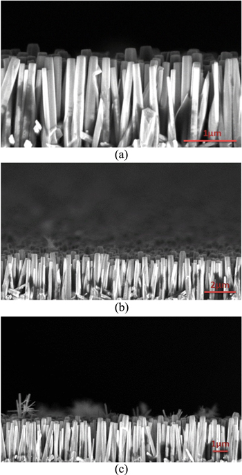
Figure 1. Cross-sectional SEM images of the vertical ZnO nanowires grown with different lengths (a) 1 μm, (b) 2 μm, (c) 3 μm.
Download figure:
Standard image High-resolution image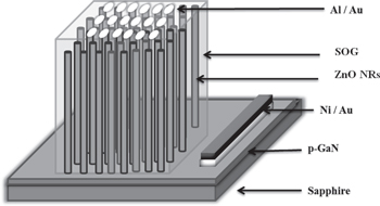
Figure 2. Schematic diagram of the n-ZnO NRs/p-GaN heterojunction LEDs.
Download figure:
Standard image High-resolution imageThe EL emission spectra for the fabricated n-ZnO NRs/p-GaN heterojunction LEDs at a bias voltage of 10 V are shown in figure 3. The EL spectrum of LED I reveals three kinds of emission peaks—a broad deep band emission centered at 620 nm, a peak centered at 455 nm (violet-blue) and a UV peak at 390 nm. Concerning the origin of emission under forward bias, the UV emission originates from the band-to-band recombination of free excitons, while the deep band emission is attributed to the falling of electrons from vacancy-related deep bands to the valence band in the ZnO NRs [21–23]. Similarly, the EL spectrum of LED II exhibits a relatively weak UV peak centered at 395 nm and two visible deep band emissions with peaks centered at 460 nm and 625 nm. The emission spectrum of LED III contains only two visible deep band emissions with peaks centered at 455 nm and 620 nm. By comparing the emission bands of the different LEDs, it is clear that by increasing the length of the ZnO NRs, the relative intensity of the visible deep band emission increases, whereas the contribution of the UV band emission decreases and finally disappears. The ratio of the visible deep band emission to the UV emission was previously reported to depend on the size of the ZnO nanostructures, and the UV emission from the ZnO NRs has been reported to be internally reabsorbed within 2 μm [24, 25]. Yong Sun et al reported a temperature-dependent red shift in ZnO spectra which was attributed to the local thermal effect [26]. The EL spectrum of LED II has a 5 nm red shift which might be because the sample is heated during measurements.
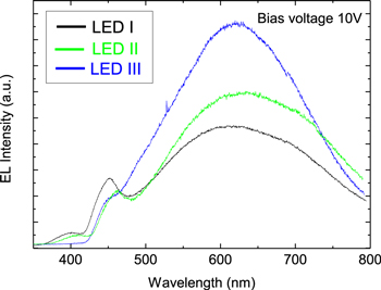
Figure 3. Room temperature EL spectrum for n-ZnO NRs/p-GaN heterojunction LEDs at 10 V.
Download figure:
Standard image High-resolution imageCL spectroscopy was performed to further study the UV emission and reabsorption characteristics of the ZnO NRs. Figure 4 shows the CL spectra for ZnO NRs of different lengths. For these CL measurements, a beam of electrons was projected onto the top surfaces of the studied ZnO NRs at the same accelerating voltage. The CL spectrum of LED I exhibits two emission peaks centered at 388 nm and 685 nm; these peaks are associated with UV and visible deep band emission peaks respectively. The CL spectrum of LED II also consists of two emission peaks centered at 388 nm and 685 nm corresponding to UV and visible deep band emission. The CL spectrum of LED III exhibits only one visible deep band emission peak centered at 685 nm. By comparing the emission bands of the different LEDs, it becomes evident that the intensity of the visible deep band emission increases with an increase in the length of the ZnO NRs, whereas the intensity of the UV band emission decreases and finally disappears. The variation in the peak positions in the CL and EL spectra is due to heating the samples by electron bombardment during the CL measurements. It becomes clear by comparing the emission bands of all the LEDs that the relative intensity of the visible deep band emission increases whereas the UV band emission decreases and finally disappears with the increasing length of the ZnO NRs.
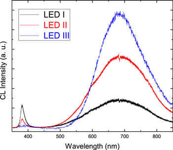
Figure 4. Room temperature CL spectra of ZnO NRs taken at a spot size of 50 nm.
Download figure:
Standard image High-resolution imageTo clarify the specific contributions of different parts of the ZnO NRs, we conducted depth resolved CL spectroscopy studies. In this technique, the CL penetration depth increases with an increase in the electron beam energy, as determined by the energy-range relationships for energy loss within solids [27, 28]. Bano et al reported the curve of energy loss per unit depth (dE/dx) as a function of depth into the ZnO [25]. These curves present a polynomial fit to the Everhart–Hoff depth dose relation [27]. CL signals from different depth positions within the band gap of the material can be excited and thus an average depth distribution of luminescence can be determined. The penetration depth of the electron beam increases with an increase in the acceleration voltages, and in the present study the acceleration voltage was in the 10–30 kV range. Using the Kanaya–Okayama model, the penetration depth was calculated to be 0.04–2.16 μm, corresponding to the acceleration voltage in the 10–30 kV range [25–28]. Figure 5 demonstrates the normalized CL spectra of LED II for the beam current of 180 pA and different accelerating voltages (10–30 kV). The CL spectra exhibit visible deep band emission centered at 685 nm and UV emission at 388 nm. The electron acceleration voltages of 20 kV and 30 kV correspond to the penetration depths of 1 μm and 2.16 μm, respectively [25, 27]. The electron beam is expected to penetrate deeper into the ZnO NRs with an increase in the accelerating voltage. Figure 5(a) shows that the UV emission decreases and the visible deep band emission increases with an increase in the penetration depth of the electron beam, which demonstrates that defect concentrations vary in orders of magnitude with depth on a nanometer scale. The CL intensities of the UV and visible deep band emissions as a function of penetration depth are shown in figure 5(b). The UV and visible deep band emissions show distinct differences in depth dependence. The electron beam is expected to penetrate deeper in the ZnO material and excite more electron–hole pairs near and below the penetration depth. In this way, more and more emission centers will be excited by the electron bombardment. It is reported that the extraction factor for ZnO can be low due to its high absorption coefficients (∼2 × 105 cm−1), which increases the probability of UV reabsorption within the crystal itself [29–31]. This reabsorbed UV can excite defect states in the structures, resulting in visible deep band emission. Thus, a part of the UV emission may contribute to the enhancement of visible deep band emission [32]. Remarkably, the ratio of the UV to the visible deep band emission intensity, which is used as a criterion for the quality of the ZnO NRs, decreases with the penetration depth within the whole length of the ZnO NRs, as shown in figure 5(b). Figure 5(b) shows that the defects responsible for the visible deep band emission are not confined near the surface but are ubiquitous inside the ZnO NRs. In our previous report, we have reported that the UV emission from ZnO NRs can be internally reabsorbed within the material [25]. This can excite deep defect states in ZnO NRs, validating the fact that part of the generated UV emission contributes to the enhancement of the emission intensity of the visible deep band.
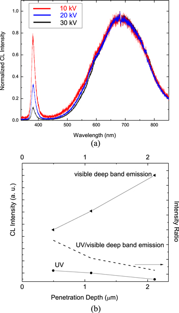
Figure 5. (a) Normalized depth-dependent CL spectra of ZnO NRs at acceleration voltages from 10–30 kV. (b) The emission intensity (right axis) of the UV and visible deep band emission, as well as the ratio of UV and visible deep band emission (left axis) as a function of penetration depth.
Download figure:
Standard image High-resolution imageTo confirm the dependence of LED EQE on the length of the ZnO NRs, the photocurrent–voltage characteristics of the fabricated n-ZnO NRs/p-GaN heterostructure LEDs were measured. Figure 6(a) shows that for all considered devices, the emitted light can be captured as a photocurrent that is detected using a photodiode. Figure 6(a) illustrates that the photocurrent increases with an increase in the length of the ZnO NRs; this measurement indicates that the emission of photons increases with an increase in the length of the ZnO NRs. The EQE is defined as the ratio of the number of photons emitted by an LED to the number of electrons injected into the LED. Figure 6(b) shows the EQE verses voltage plot for the fabricated n-ZnO NRs/p-GaN heterostructure LEDs. The EQEs of LED1, LED2 and LED3 were calculated as 2.07%, 2.81% and 3.88% at a voltage of 10 V (30 μA), respectively, suggesting that increasing the length of the ZnO NRs can increase the EQE by 87%. The radiative defects and EQE of the ZnO NRs depends critically on the growth conditions. Therefore high EQE values can be achieved by optimizing the ZnO NR growth time and temperature with more defects that contribute to radiative emission [30]. In this study the length of the ZnO NR arrays was controlled by varying the growth time. Such a strong increase in photon emission and EQE likely occurs because increasing the length of the ZnO NRs strongly confines the injected carriers and the emitted UV is reabsorbed by the ZnO NRs to excite more electrons. These results confirm that the EQE of n-ZnO NRs/p-GaN heterostructure LEDs depends on the length of the ZnO NRs.
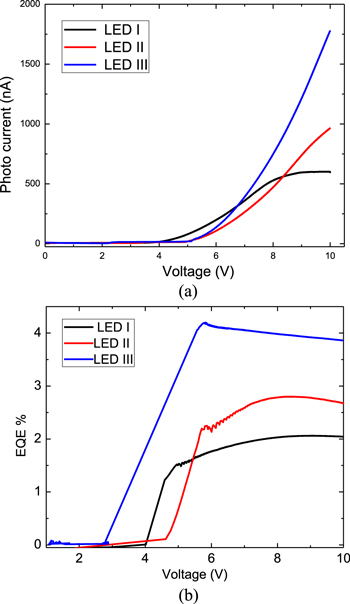
Figure 6. (a) The photocurrent–voltage characteristics of the n-ZnO NRs/p-GaN heterostructure LEDs. (b) EQE–voltage characteristics of the n-ZnO NRs/p-GaN heterostructure LEDs.
Download figure:
Standard image High-resolution imageThe CRI is a measure of the quality of chromatic light, therefore CRI values were calculated for the fabricated n-ZnO NRs/p-GaN heterostructure LEDs. Figure 7 shows the CIE 1931 color map chromaticity diagram in the (x, y) system of coordinates. The CRI values of LED I, II, and III were calculated to be 90, 95 and 98 respectively. It clearly shows that the CRI increases with an increase in the length of the ZnO NRs, suggesting that the quality of light emitted by LEDs can be tuned by varying the length of the ZnO NRs.

Figure 7. The chromaticity diagram of the fabricated LEDs, LED1(■), LED2 (★), LED3(●).
Download figure:
Standard image High-resolution image
Conclusions
In conclusion, we have demonstrated a viable and highly promising approach to enhance the EQE and quality of n-ZnO NRs/p-GaN LEDs by adjusting the length of ZnO NRs. Depth-resolved CL spectroscopy revealed that the UV emission decreased and visible deep band emission increased with an increase in the penetration depth of the electron beam. The emitted UV was reabsorbed by the ZnO NRs, exciting additional defect states and thus increasing the emission intensity of the visible deep band. The photocurrent measurements confirmed that the emission of photons increases with an increase in the length of the ZnO NRs, increasing the EQE by 87%, which indicates that the EQE of n-ZnO NRs/p-GaN heterostructure LEDs depends on the size of the ZnO NRs. The color map chromaticity diagram clearly shows that the CRI of the fabricated LEDs increases with an increase in the length of ZnO NRs, indicating that the quality of light generated by LEDs can be tuned by varying the length of ZnO NRs. Therefore, the results of all these measurements corroborate the idea that the EQE and light quality of n-ZnO NRs/p-GaN heterostructure LEDs depend on the length of the ZnO NRs. These results and conclusions are likely to be useful for optimizing the LED fabrication process, and subsequently obtaining tunable white LEDs.
Acknowledgments
This research project was supported by a grant from the 'Research Center of the Female Scientific and Medical Colleges, Deanship of Scientific Research', King Saud University.